Finger-gate manipulated quantum transport in a semiconductor narrow constriction
with spin-orbit interactions and Zeeman effect
Abstract
The authors investigate quantum transport in a narrow constriction fabricated by narrow band gap semiconductor materials with spin-orbit (SO) couplings. We consider the Rashba-Dresselhaus (RD) spin-orbit interactions (SOIs) and the Zeeman effect induced by an in-plane magnetic field along the transport direction. The interplay of the RD-SOI and the Zeeman effect may induce a SOI-Zeeman gap and influence the transport properties. We demonstrate that an attractive scattering potential may induce electron-like quasi-bound-state feature and manifest the RD-SOI-Zeeman induced Fano line-shape in conductance. Furthermore, a repulsive scattering potential may induce hole-like quasi-bound-state feature on the subband top of the lower spin branch.
pacs:
73.23.-b, 72.25.Dc, 72.30.+qI Introduction
Quantum transport involving interference nature of charged particle can be realized by using the split-gates induced narrow constriction connecting the source and drain Ohmic contacts. The conductance through the narrow constriction is known to be quantized when the Fermi level of the system is tuned energetically by applying a voltage to a nearby gate.Wees1988 ; Wharam1988 The quantization features can be explained within the framework of simple noninteracting models,Landauer1970 ; Buttiker1990 ; Beenakker1991 and the conductance depends only on the transmission coefficient. The related quantum devices can be utilized in various applications including the prototypes of quantum information processing.Loss1998
Spin-orbit interaction (SOI) is a relativistic effect, in which a charged particle moving with direction perpendicular to an electric field experiences an effective magnetic field that couples to the spin degree of freedom of the moving particle. Various spin-orbit (SO) effects present in semiconductor structures provide a promising way to spin manipulation in two-dimensional (2D) electron gases.Winkler2003 ; Meier2007 Band structure behaviors and transport properties involving SOI in semiconductor quantum structures have received much interest due to its important application in the emerging field of spintronic devices.Datta1990 ; Zutic2004 ; Bandyopadhyay2004 Manipulating the spin degree of freedom offers the possibility of devices with high speed and very low power dissipation that is one of the essential requirement for the applications in quantum computing and memory storage.Wolf2001 ; Awschalom2002
The SOI can be induced when the transporting electron experiences a strong electric field due to the asymmetry in the confinement potential, namely the structure inversion asymmetry (SIA) induced Rashba SOI.Rashba60 Especially, the Rashba SOI may be significantly induced in two-dimensional electron gases (2DEGs) confined by asymmetric potential in semiconductor materials. Experimentally, the Rashba interaction has been shown to achieve electron spin manipulation by using bias-controlled gate contacts.Nitta1997
In addition to the Rashba effect, there is also a Dresselhaus SOI caused by the microscopic electric field arising from the lack of inversion symmetry in the Bravais lattice, namely the bulk inversion asymmetry (BIA).Dresselhaus1955 The combined effect of the Rashba and Dresselhaus SOI affects significantly the spin related properties and should be considered when analyzing the performance of spin-resolved electronic devices. Recently, several approaches were proposed to engineer the spin-resolved subband structure utilizing magnetic fieldsMuccio02 ; Brataas02 ; Zhang03 ; Wang03 or ferromagnetic materials.Sun03 ; Zeng03 The SOI and in-plane magnetic field induced Zeeman effect may modify the subband structure leading to SOI-Zeeman subband gap feature.Pershin2004 ; Quay2010 However, how the scattering potentials influence the spin-resolved quantum transport and its interplay with the SOI-Zeeman interactions has not yet been explored.
In this work, we consider a split-gate induced narrow constriction that is fabricated in a 2D quantum well with narrow band gap semiconductor material. Both the Rashba and Dresselhaus SOIs as well as an applied external in-plane magnetic field are taken into account to investigate the influences of the subband structures. Moreover, we apply a narrow finger gate to affect the ballistic transport properties. Below, we shall demonstrate analytically and numerically that tuning the strength of the applied in-plane magnetic field as well as the Rashba and the Dresselhaus SO-coupling constants to manipulate the subband structures leading to fruitful quantum transport properties.
This article is organized as follows. In Sec. II, we shall describe our theoretical model including the Rashba and Dresselhaus SOIs as well as an external in-plane magnetic field. Section III investigates the spin-resolved quantum transport properties. Concluding remarks will be presented in Sec. IV.
II model and subband structures
The system under investigation is assumed to be a narrow band gap InAs-In1-xGaxAs semiconductor heterostructure grown in crystallographic direction. We consider the conduction band of a 2D quantum well within the effective mass approximation. We select the length unit is the inverse of the Fermi wave number , and the energy unit is the Fermi energy with and being, respectively, the effective mass of an electron and the reduced Planck constant. Correspondingly, the magnetic field is in units of with being the Bohr magneton, and the Rashba and Dresselhaus SO-coupling constants are in units of . By using the above units, all physical quantities presented below are dimensionless.Tang1996
A pair of split gates is applied in the transverse direction forming a quantum channel described by the unperturbed Hamiltonian
| (1) |
that consists of a 2D kinetic energy term and a confining potential energy term
| (2) |
where indicates the width of the quantum channel. The transported electron is supposed to be affected by the effects of SO interaction and the external in-plane magnetic field, and hence can be described by the effective unperturbed Hamiltonian
| (3) |
Here we have assumed that the magnetic field is applied in the transport direction such that the Zeeman interaction is simply , in which the factor with being the effective gyromagnetic factor ( for InAs). In order to manipulate the spin-resolved quantum transport properties, we apply a finger gate on top of split gate with an insulator in between, as illustrated in Fig. 1. We assume that the finger gate is sufficiently narrow and then can be described by a delta scattering potential form . The whole quantum channel system under investigation is thus described by the total Hamiltonian .
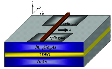
The SOI term in Eq. (3) consists of the Rashba and Dresselhaus SOI effects . For the transport direction , the Rashba SO Hamiltonian is given by the -linear form
| (4) |
where ( = {}) are the Pauli matrices and is the 2D electron wave vector. The Rashba coupling strength is proportional to the electric field along direction perpendicular to the 2D electron gas. In general, the Dresselhaus interaction has a cubic dependence on the momentum of the carriers. For a narrow semiconductor quantum well grown along the direction, it reduces to a 2D linear momentum dependent form
| (5) |
where the Dresselhaus coupling strength is determined by the semiconductor material and the geometry of the sample. The spin-orbit coupling contributions can be simplified as in a narrow quantum channel.
The eigenfunction of Eq. (3) can be expressed as the multiplication of the spatial wave functions and the spinor state ,
| (6) |
where the transverse wave function in the subband is of the form
| (7) |
with unperturbed subband energy due to the bare confining potential. The corresponding eigenenergies can be obtained
II.1 Rashba-Zeeman effects
In the absence of the Dresselhaus SOI, the Dresselhaus coupling strength is identically zero. In this subsection, we focus on the the Rashba-Zeeman (RZ) effect, in which the spin resolved subband energies can be obtained analytically Wang2006
| (8) |
and the spinor states
| (9) |
where indicates the upper () and lower () spin branches and describes the momentum dependent spin orientation of an electron. Defining the group velocity of an electron in the spin branch
| (10) |
allows us to determine the local minimum (subband bottom) and local maximum (subband top) in the subband structures by setting the group velocity to be identically zero.
The calculations presented below are carried out under the assumption that the electron effective mass , which is appropriate to the InAs-In1-xGaxAs semiconductor interface with the typical electron density cm-2.Nitta1997 Accordingly, the length unit is = = 5.0 nm, the energy unit is = = 66 meV, and the spin-orbit coupling parameters are in units of eVm. Below, we select the width of the narrow constriction nm so that the unperturbed subband energy is simply . Moreover, the range of the variation of energy is smaller than the second unperturbed subband energy, namely . Furthermore, sufficient low temperature is required to avoid thermal broadening effect, that is, (or K). We note in passing that the width of the scattering potential should be less than the Fermi wave length nm to be described as a delta potential. We assume high-mobility semiconductor materials and, hence, the impurities and defects can be neglected.
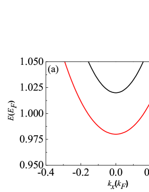
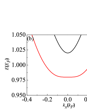
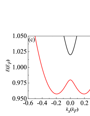
The energy spectrum for the case of RZ effect with different coupling strength regimes is illustrated in Fig. 2. Before we illustrate the subband gap features, it should be reminded that the Zeeman effect is to induce an energy gap between the opposite spin branches. For the case of weak Rashba SO coupling, namely , both the spin branches have only subband bottoms at with energies at . The subband energy spacing between the upper () branch and the lower () branch is the Zeeman splitting = . Hence the RZ-SO gap is dominated by the Zeeman effect in the weak SO coupling regime.
For the case of strong Rashba coupling , the subband bottom of the upper spin branch is still at . However, the subband bottom at of the lower spin branch becomes a subband top with the same energy . Therefore, the subband energy spacing between the and branches is still but forming a subband gap. In addition to the subband top in the lower subband branch, there are two subband bottoms at with the same energy .
We note in passing that if only the Rashba effect is considered, the subband structure is simply . Also, the subband structure manifests only lateral splitting in momentum , where the subband bottoms of spin branches are at the wave numbers with the same energy .
In order to investigate the transport properties, one has to determine the propagating and evanescent modes for a given energy. To this end, it is convenient to rewrite the energy dispersion relation in the following form
In general, this equation determines four complex values corresponding to either propagating or evanescent modes.
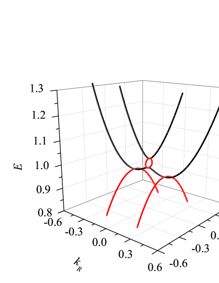
In Fig. 3, we show the energy dispersion obtained from Eq. (II.1) in the complex wave number space for the case of so that subband gaps can be generated. It is clearly shown that there are four evanescent modes when the electron energy is less than the lower subband bottom. When the electron energy is greater than the lower subband bottom and below the subband gap, there four propagating modes. It is interesting to notice that when electron energy is within the subband energy gap regime, there are two propagating modes and two evanescent modes (the red bubble in Fig. 3). Although the conductance calculated later only summing over the propagating modes, sufficient number of evanescent modes should be taken into account to achieve numerical accuracy when we calculate the intermediate scattering processes.
II.2 Rashba-Dresselhaus-Zeeman effects
In the presence of Rashba and Dresselhaus SOI with an in-plane magnetic field along the transport direction, the electronic system can be described by
| (12) |
For electrons incident from the subband , the spinor states satisfies the matrix equation
| (15) | |||
| (16) |
The energy spectrum can be easily obtained of the form
| (17) |
This equation is convenient to obtain energy spectrum as a function of real wave vector for propagating modes.
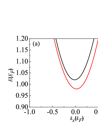
In Fig. 4, we show the Dresselhaus effect correction to the Rashba SOI by fixing the strength of Zeeman effect ( = 0.02) and tuning the strength of Rashba and Dresselhaus SOI. To analyze the the subband structures, it is convenient to introduce the Rashba-Dresselhaus (RD) SO-coupling constant , namely , for defining different coupling regimes. Figure 4(a) demonstrates the weak SO coupling regime . It is clearly shown that the spin-split subband structure is slightly asymmetric due to the Dresselhaus effect. The subband bottoms of both subband branches are no longer at zero wave number. Instead, the energy bottoms are located at and . The two spin branches of a subband manifests a Zeeman splitting . Hence, in the weak coupling regime, the Zeeman effect dominates the subband structure and the RD coupling slightly let the subband structure form an asymmetric lateral shift in opposite direction for the spin branches.
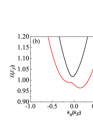
Figure 4(b) illustrates the case of intermediate SO coupling regime , it is shown that the lower spin branch becomes a shoulder subband structure at and a clear subband bottom at . On the other hand, the subband bottom of the upper branch is at , and hence the spin branches form a shoulder gap feature .
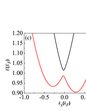
In Fig. 4(c), we show the case of strong SO coupling regime (). In this regime, it is interesting that the lower spin branch manifests three extreme values in energy. First, the left subband bottom of the upper spin branch is at = . Second, the right subband bottom is at = . Third, the subband top of the lower subband branch is at . On the other hand, the subband bottom of the upper branch is at . Therefore, the subband gap in the strong coupling regime is around . This implies that reduction of the subband gap due to the Dresselhaus effect is a nontrivial effect.
III quantum transport properties
In this section, we shall investigate the quantum transport properties subject to spin-orbit interactions and Zeeman effect in a narrow constriction. We assume that the quantum channel is sufficiently narrow and focus on the first two conductance steps associated with the two spin branches of an electron. Below, we shall explore how the spin-mixing effect due to the SOI-Zeeman coupling influences the transport properties.
III.1 Rahsba-Zeeman effects
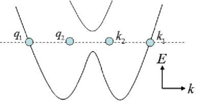
To consider an electron incident along the transport direction , it is convenient to denote the wave number of right-going (left-going) modes as , in which the subscript could be by “1” or “2” indicating the “outer” or the “inner” modes, as illustrated in Fig. 5. The scattering wave function for an electron incident from the source electrode can be written of the form
| (18) |
| (19) |
Here we have omitted the subband index for simplicity. By taking into account the spin branches as well as the spin-flip scattering mechanisms, the scattering wave functions can be generally expressed as
| (27) | |||||
| (28) |
where and with = are the spinor elements of the incident wave. In addition, and = with = are the spin-state elements of the reflection wave. Moreover, the spin-state elements of the spin-flip transmission wave are given by
| (29) |
and
| (30) |
Similarly, we can obtain the spin-state elements of the spin-flip reflection wave, given by
| (31) |
and
| (32) |
By matching the boundary conditions at around the scattering potential induced by the finger gate, it is easy to obtain the matrix equation of motion for the spin-resolved transport involving the finger-gate induced spin-flit scattering
| (41) | |||
| (46) |
To calculate conductance in the noninteracting electron model we employ the framework of Landauer-Büttiker formula.Landauer1970 ; Buttiker1990 For a given energy, solving for the spin non-flip and flip reflection coefficients and , as well as the spin non-flip and flip transmission coefficients and , we can thus express the zero temperature conductance as
| (47) |
Here = is the conductance quantum of a single spin branch, and and indicate, respectively, the spin branches of the incident and transmission waves in the left and right leads. Therefore, and represent the group velocity at the corresponding modes.
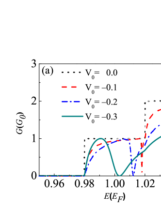
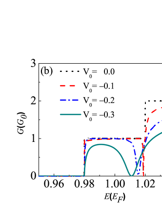
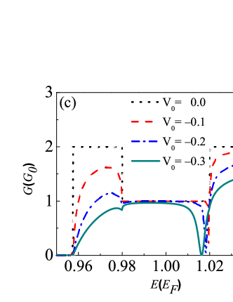
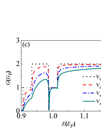
In Fig. 6, we demonstrate the transport properties in the presence of an attractive scattering potential due to the finger gate by fixing the in-plane magnetic field ( = 0.02) while tuning the strength of Rashba SOI. In general, the attractive scattering potential plays a role to suppress the conductance. we present the conductance as a function of electron energy with different strength of attractive potential: (dotted), (dashed), (dash-dotted), (solid). Here, we fix the Zeeman effect to be = 0.02, in other words the magnetic field T if the factor = for InAs-based material. Moreover, we tune the Rashba parameter: (a) = 0.05 (, weak SO coupling); (b) = 0.1 (, intermediate SO coupling); (c) = 0.2 (, strong SO coupling).
Figure 6(a) illustrates the transport properties in the weak SO coupling regime (). When the attractive potential is weak (), the conductance manifests a clear dip structure and form an electron-like quasibound state at the subband bottom of the upper spin branch. When the potential strength increases (), the dip structure becomes a broad valley structure and is shifted toward the low energy regime indicating the shorter life time. This broadening effect is suppressed in the mediate SO coupling regime (), as shown in Fig. 6(b). It is interesting to notice in Fig. 6(c) that the conductance manifests an abrupt drop to unity in the energy regime due to the spin-gap feature as shown previously in Fig. 2(c). It is interesting that the conductance dip structure is not broadened for larger scattering potential . This indicates that the life time of the quasibound state feature is enhanced in the strong Rashba SO coupling regime.
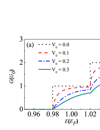
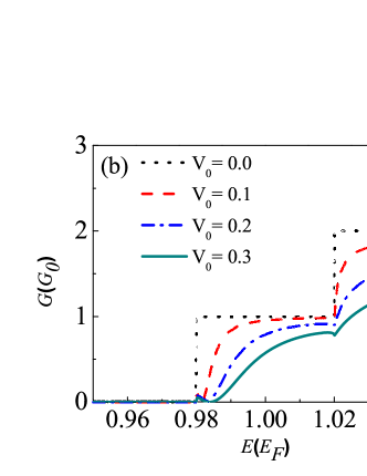
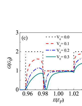
In Fig. 7, we demonstrate the transport properties in the presence of a repulsive scattering potential due to the finger gate by fixing the in-plane magnetic field ( = 0.02) while tuning the strength of Rashba SOI. In general, the repulsive potential plays a role to strongly suppress the conductance in the low kinetic energy regime. we exhibit the conductance as a function of electron energy with different strength of repulsive scattering potential: (dotted), (dashed), (dash-dotted), (solid). Here, we fix the Zeeman effect to be = 0.02, namely the magnetic field T if the factor = for InAs-based material. Then we tune the strength of the Rashba SOI: (a) = 0.05 (, weak SO coupling); (b) = 0.1 (, intermediate SO coupling); (c) = 0.2 (, strong SO coupling).
For the case of weak SO coupling regime shown in Fig. 7(a), the conductance is strongly suppressed in the low kinetic energy regime and behaves monotonically increasing. For the case of intermediate SO coupling regime shown in Fig. 7(b), the conductance is more strongly suppressed in the low kinetic energy regime than the case of weak SO coupling regime. It is interesting to notice when the repulsive is strong enough () the conductance is even suppressed to zero at energy . This is a clue of hole-like quasi-bound-state feature with very short life time due to the shoulder-like structure of the lower subband branch shown in Fig. 7(b). For the case of strong SO coupling regime, since the subband structure can form a subband gap, as is shown in Fig. 7(c), it allows to form a significant hole-like quasi-bound-state feature at the subband top of the lower spin branch. The conductance thus manifests a dip structure energy .
III.2 Rashba-Dresselhaus-Zeeman effects
In this subsection we shall explore the transport properties of a narrow constriction by fixing the Zeeman effect while manipulating the strength of the RD-SOI and tuning the amplitude of scattering potential that can be either attractive or repulsive. All the physical parameters shown bellow are the same with the physical parameters in the previous subsection discussing the case of R-SOI. The transport calculation for the case of RD-SOI is similar to the case of R-SOI but has to be solved numerically not shown here.
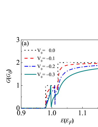
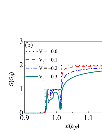
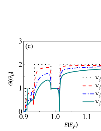
In Fig. 8, we investigate how an attractive scattering potential influences the transport properties by tuning Rashba and the Dresselhaus effects and fixing the in-plane magnetic field, the corresponding energy spectra are shown in Fig. 4. The conductance is presented as a function of electron energy with different strength of attractive scattering potential: (dotted), (dashed), (dash-dotted), (solid). We fix the in-plane magnetic field so that the Zeeman effect = 0.02. In addition, the Rashba and Dresselhaus SO-coupling constants are selected to cover three coupling regimes: (a) = 0.02 (, weak SO coupling regime); (b) = 0.1 (, intermediate SO coupling regime); (c) = 0.2 (, strong SO coupling regime).
For the case of weak SO coupling regime shown in Fig. 8(a), the attractive scattering potential may induce a Fano structure in conductance. This is because a true-bound-state can be induced by the attractive scattering potential at energy , in which the binding energy = = (dashed), (dash-dotted), and (solid). The Fano structure is at for potential . It is interesting to notice that the bounded upper spin-branch electron bounded energy interfere with the extended lower spin-branch electron and form the RD-Zeeman induced Fano structure. For the case of intermediate SO coupling regime shown in Fig. 8(b), we can see clear quasi-bound-state feature at the subband bottom of the upper spin branch. For the case of strong SO coupling regime shown in Fig. 8(c), the Fano structure is red-shifted to for potential . In the SOI-Zeeman induced subband gap region, we see a more significant quasi-bound-state formed at around .
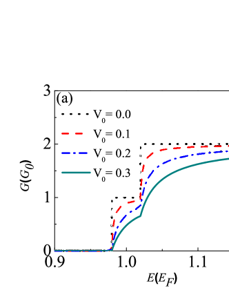
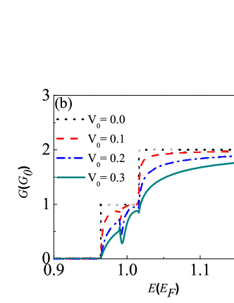
In Fig. 9, we investigate how a repulsive scattering potential influences the transport properties by tuning Rashba and the Dresselhaus effects and fixing the in-plane magnetic field, the corresponding energy spectra are shown in Fig. 4. The conductance is plotted as a function of electron energy with different strength of repulsive scattering potential: (dotted), (dashed), (dash-dotted), (solid). We fix the in-plane magnetic field so that the Zeeman effect = 0.02. In addition, we tune the Rashba and Dresselhaus SO-coupling constants as (a) = 0.02 (, weak spin-orbit coupling regime); (b) = 0.1 (, intermediate spin-orbit coupling regime); (c) = 0.2 (, strong spin-orbit coupling regime).
For the case of weak SO coupling regime shown in Fig. 9(a), the repulsive scattering potential cannot form bound states even for the case of strong potential amplitude , in which the conductance behaves monotonically increasing and the conductance is suppressed to . For the case of intermediate SO coupling regime shown in Fig. 9(b), it is interesting to note that the conductance manifests a hole-like quasi-bound-state feature on the top of shoulder subband top (), as is shown in Fig. 4(b). For the case of strong SO coupling regime shown in Fig. 9(c), the general feature in conductance is the strong drop from to in the subband gap of the two spin branches. Moreover, it is clearly shown that the hole-like quasi-bound-state feature can be induced on the subband top of the lower spin branch and form a very clear dip structure in conductance.
IV Concluding Remarks
We consider a narrow constriction with the Rashba and Dresselhaus spin-orbit interactions under an in-plane magnetic field applied in the transport direction. A top finger gate is used to generate an attractive or a repulsive scattering potential. This allows us to investigate the coherent quantum transport properties involving spin-flip scattering. The competition of the spin-orbit scattering and the Zeeman effect plays an important role to the subband structures and the transport properties. The Zeeman effect allows us to separate the R-SOI and RD-SOI into three regimes: the weak, mediate, and strong SO coupling regimes.
In the weak SO coupling regime with Zeeman effect, the subband structure remains the quadratic form. It is symmetric if only the Rashba SOI dominates while asymmetric if both the Rashba and Dresselhaus SOIs are significant. For the case of attractive potential with only the Rashba SOI, it allows electron occupying the upper spin branch to form a true-bound-state feature with binding energy , and the conductance manifests a valley structure. It is important to note that the presence of both the Rashba and the Dresselhaus SOIs may enhance the interference between the localized upper spin branch state and the extended lower spin branch state, and hence the conductance manifests a Fano structure. For the case of repulsive potential the conductance behaves monotonically increasing for both R-SOI and RD-SOI.
In the intermediate SO coupling regime with Zeeman effect, the subband structure of the lower spin branch exhibits a quadratic structure for R-SOI and a shoulder-like structure for RD-SOI. For the case of attractive potential with R-SOI, the conductance manifests a quasi-bound-state feature below the upper branch. Moreover, for the case of attractive potential with RD-SOI, we have found a kink structure in conductance at the shoulder of the lower spin branch. For the case of repulsive potential with R-SOI, the conductance is strongly suppressed and monotonically increasing. However, for the case of repulsive potential with RD-SOI, the conductance can manifest a clear hole-like quasi-bound-state feature.
In the strong SO coupling regime with Zeeman effect, the subband structure of the lower spin branch exhibits a subband top structure for both the R-SOI and RD-SOI. In addition, the two subband bottoms of the lower spin branch with same energy for R-SOI and with different energy for RD-SOI. For the case of attractive potential with R-SOI, the conductance manifests a quasi-bound-state feature below the upper branch. However, the conductance structure for the case of attractive potential with RD-SOI is more complicated. We have found a true-bound-state feature in conductance with Fano line shape depending on the strength of scattering potential. This behavior is due to the different energy of two subband bottoms in the lower spin branch. In addition, an electron-like quasi-bound-state can be found at the subband bottom of the upper spin branch. For the case of repulsive potential with R-SOI, we have found clear hole-like quasi-bound-state feature at the subband top of the lower spin branch. This hole-like quasi-bound-state feature is more significant with longer life time for the case of repulsive potential with RD-SOI.
In conclusion, we have investigated the interplay of Rashba-Dresselhaus spin-orbit interaction and the in-plane magnetic field induced Zeeman effect to influence the spin-resolved coherent transport. By tuning the finger gate, we have demonstrated how the attractive and repulsive scattering potentials affect the conductance features. We have analyzed in detail the nontrivial subband and quantum transport properties concerning the SOI-Zeeman induced electron-like and hole-like quasi-bound-state features.
Acknowledgements.
This work was supported by the National Science Council in Taiwan under Grants No. NSC100-2112-M-239-001-MY3, No. NSC-98-2112-M-009-011-MY2, and No. NSC-100-2112-M-009-013-MY2. We are thankful to the technical support from Shu-Jui Yu.References
- (1) B. J. van Wees, H. van Houten, C.W. J.Beenakker, J. G.Williamson, L. P. Kouwenhoven, D. van der Marel, and C. T. Foxon, Phys. Rev. Lett. 60, 848 (1988).
- (2) D. A. Wharam et al., J. Phys. C: Solid State Phys. 21, L209 (1988).
- (3) R. Landauer, Philos. Mag. 21, 863 (1970).
- (4) M. Büttiker, Phys. Rev. B 41, 7906 (1990).
- (5) C.W. J. Beenakker and H. Van Houten, Solid State Phys. 44, 1 (1991).
- (6) D. Loss and D. P. Divincenzo, Phys. Rev. A 57, 120 (1998).
- (7) R. Winkler, Spin-Orbit Coupling Effects in Two-Dimensional Electron and Hole Systems, Springer Tracts in Modern Physics Vol. 191 (Springer, Berlin, 2003).
- (8) L. Meier, G. Salis, I. Shorubalko, E. Gini, S. Schon, and K. Enslin, Nat. Phys. 3, 650 (2007).
- (9) S. Datta and B. Das, Appl. Phys. Lett. 56, 665 (1990).
- (10) I. utić, J. Fabian, and S. Das Sarma, Rev. Mod. Phys. 76, 323 (2004).
- (11) S. Bandyopadhyay and M. Cahay, Appl. Phys. Lett. 85, 1814 (2004).
- (12) S. A. Wolf et al., Science 294, 1488 (2001).
- (13) Semiconductor Spintronics and Quantum Computation, edited by D.D. Awschalom, N. Samarth, and D. Loss (Springer-Verlag, Berlin, 2002).
- (14) E. I. Rashba, Sov. Phys. Solid State 2, 1109 (1960); Y. A. Bychkov and E. I. Rashba, J. Phys. C 17, 6039 (1984).
- (15) J. Nitta, T. Akazaki, H. Takayanagi, and T. Enoki, Phys. Rev. Lett. 78, 1335 (1997).
- (16) G. Dresselhaus, Phys. Rev. 100, 580 (1955).
- (17) E. R. Mucciolo, C. Chamon, and C. M. Marcus, Phys. Rev. Lett. 89, 146802 (2002); S. K. Watson, R. M. Potok, C. M. Marcus, and V. Umansky, ibid. 91, 258301 (2003).
- (18) A. Brataas, Y. Tserkovnyak, G. E. W. Bauer, and B. I. Halperin, Phys. Rev. B 66, 60404 (2002).
- (19) P. Zhang, Q. K. Xue, and X. C. Xie, Phys. Rev. Lett. 91, 196602 (2003).
- (20) B. G. Wang, J. Wang, and H. Guo, Phys. Rev. B 67, 092408 (2003).
- (21) Q. F. Sun, H. Guo, and J. Wang, Phys. Rev. Lett. 90, 258301 (2003).
- (22) W. Zeng, J. L. Wu, B. G. Wang, J. Wang, Q. F. Sun, and H. Guo, Phys. Rev. B 68, 113306 (2003).
- (23) Y. V. Pershin, J. A. Nesteroff, and V. Privman, Phys. Rev. B 69, 121306(R) (2004).
- (24) C. H. L. Quay, T. L. Hughes, J. A. Sulpizio, L. N. Pfeiffer, K.W. Baldwin, K.W.West, D. Goldhaber-Gordon, and R. de Picciotto, Nat. Phys. 6, 336 (2010).
- (25) C. S. Tang and C. S. Chu, Phys. Rev. B 53, 4838 (1996).
- (26) L. Y. Wang, C. S. Tang, and C. S. Chu, Phys. Rev. B 73, 085304 (2006).