Tuning hole mobility in InP nanowires
Abstract
Transport properties of holes in InP nanowires were calculated considering electron-phonon interaction via deformation potentials, the effect of temperature and strain fields. Using molecular dynamics, we simulate nanowire structures, LO-phonon energy renormalization and lifetime. The valence band ground state changes between light- and heavy-hole character, as the strain fields and the nanowire size are changed. Drastic changes in the mobility arise with the onset of resonance between the LO-phonons and the separation between valence subbands.
Semiconductor nanowires (NWs) are increasingly used in a wide range of devices. They appear as building blocks of nanocircuitsnanocircuit and can be applied in electrically driven lasingnaturelaser , which can be used in telecommunications and information storage for medical diagnostics and therapeuticslasrapplication . Improvements in NW synthesis, including chemical technics, allow thorough control of their shape, size and composition science279 ; lieber1 ; lieber2 ; bjork ; nano along with detailed microscopic characterization of built-in strain fields.nano ; prb As the conductivity is mostly defined by the carrier-phonon interaction and phonon-lifetime, tuning of the NW structural properties could result in the possibility of also finding optimal conditions for carrier transport.
Considerable efforts have been devoted to the description of carriers in the conduction band of NWs,cond0 ; cond1 ; cond2 ; cond4 ; cond5 ; cond6 while similar endeavors are not so common for holes in the valence band.val1 As the mobility is inversely proportional to the carrier effective mass, one may naturally expect that considering carriers in the valence band may result in a drop in mobility when compared to the light electrons in the conduction band. This could certainly be the case for heavy-hole (hh) transport; however, light-holes (lh) under certain conditions may be promoted to be the top valence band by tuning structural parameters of NWs.mariama This atypical circumstance is the result of confinement effects and hh-lh mixing, affected as well by strain and surface asymmetry fields.nano ; mariama As we will show here, this results in significant mobility enhancement for lh in suitable NWs. We can also take advantage of valence band mass anisotropy to attain resonant conditions that allow sharp variations of the hole mobility with external parameters, especially when the leading scattering process involve longitudinal optical phonons (LO-phonons) through the deformation potential.Raman2 Additional hole-phonon interactions,mahan such as deformation potential and piezoelectric coupling to acoustic phonons and polar coupling to optical phonons,Raman1 have weaker effects and will not be consider here.mahan ; cardonabook In order to provide realistic estimates of the expected mobility changes in the NWs of interest, we consider the effects of dimensionality reduction on the LO-phonon dispersion and lifetime, using molecular dynamics simulations for different NWs size and at various temperatures.
We consider different NW cross sections and shapes, while temperature effects are included in the mobility through the phonon occupation and strain effects in a multiband Luttinger Hamiltonian. We find that mobility changes in a non-monotonic fashion according to NW width, strain fields, and temperature. In particular, we show that for certain NW widths, one finds resonant behavior that greatly suppresses the hole mobility and is strongly affected by temperature and strain. The interaction potentials used in our molecular dynamics (MD) simulations consist of two- and three-body interaction terms, as described by Branicio et al.ref-md1 ; ref-md2 ; ref-md3 ; ref-md4 ; ref-md5 . The parameters of the interatomic potential are determined using the cohesive energy, density, bulk modulus and elastic constant of the material as described before,ref-md5 with some slight adjustments. foot
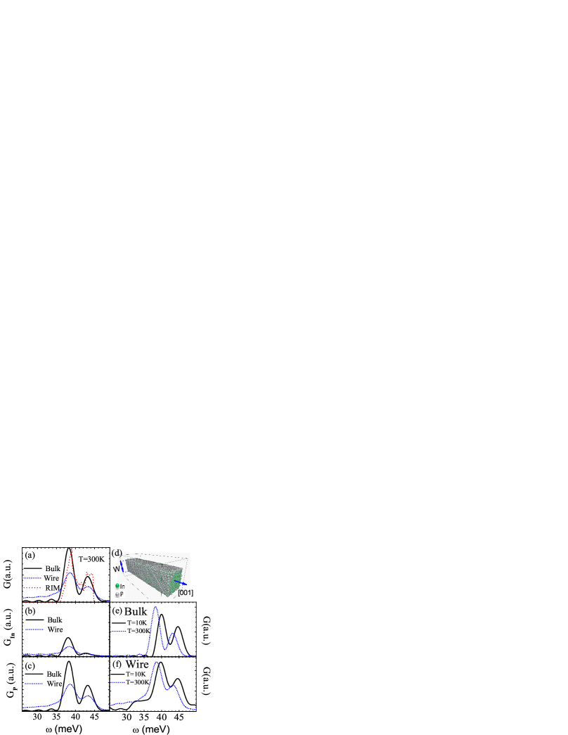
This potential provides excellent estimates for melting temperature, structural phase transformation induced by pressure, and specific heatref-md2 and describes well the vibrational density of states of the material. We obtain the phonon density of states in InP NWs considering different temperatures. The NWs were created cutting a block of a perfect crystal with the z-axis along the [001] direction with periodic boundary conditions in the z-direction. The x- and y-directions were surrounded by a vacuum region. The system consisted typically of nine unit cells along x- and y-directions and forty unit cells along the z-direction (); the total number of atoms is 25,920 (12,960 In + 12,960 P) (Fig. 1(d)). The NW is allowed to relax during a long simulation run (25,000 time steps, one time step=1.5fs) at each temperature. After this relaxation time, a few surface defects can be observed.
The velocity-velocity auto correlation function, , where is the velocity of particle at time and the brackets are averages over ensembles and particles. The vibrational phonon density of states (VDOS) is determined through the Fourier transform ref-md8
| (1) |
where the subindex is the atom In or P.
Fig. 1(a) compares the VDOS computed from MD calculations for a bulk system (solid curve) to the VDOS extracted from the rigid ion model (dashed curve) based on experimental resultsref-md6 ; ref-md7 . The MD results reproduce very well the main characteristics of the experimental, predicting the existence of the transversal optical (TO, ) and longitudinal optical (LO, ) modes, and a gap between and (acoustic modes below not shown).
The effect of the surfaces on the VDOS of the NW is also shown in Fig. 1(a)-(c). The main NW characteristics in the VDOS resemble the bulk results; however, some differences can be observed. The NW surfaces appreciably increases the amount of modes in the gap region, between and . Although the TO and LO modes are dominant, the NW surface plays an important role by inducing surface modes that appear in the gap region. We notice that the P atoms make the main contribution to the optical modes in the gap have a larger VDOS, and an overall large mode width for the NW. The optical modes are characterized by the relative displacement between ions and the lighter atoms usually dominate such modes, as shown. Moreover, we observe a slight blue shift of the LO mode () with respect to the bulk.
The effect of temperature on the VDOS for both NW and bulk structure is shown in Figs. 1(e) and (f). We see a general broadening of the modes and a shift in the peak position to lower frequencies with increasing temperature. Although the gaps region keep a similar profile, the VDOS in the gaps increase with temperature. We notice also that the temperature affects the contrast between LO and TO modes, especially in the NW, Fig. 1(f), by increasing the LO amplitude.
Notice that the mode broadening is slightly weaker for the NW than for the bulk. Based on the MD results, we verify that the TO and LO modes are the most important vibrational modes. Also, the NW exibits a shift in the LO mode with temperature, which is an important fact to be considered when calculating the contribution of hole-phonon scattering to the mobility of NWs.
The valence band Hamiltonian for the NW can describe confinement effects, mass anisotropy, and strain fields within the same framework, as one writes,luttinger
| (2) |
| (3) |
for the heavy- and light-holes, where () are the Luttinger parameters, , and . Notice that the subband with hh character along the wire has a low effective mass in the transverse direction , while the lh subband has a large transverse mass ; the different transverse masses result in the possible inversion of the lh and hh subband ordering, due to the NW confinement effects. Strain effects lead to modulation of the valence subbands,nano introducing a subband displacement given by cardona and , where , and is the spin-orbit split-off energy. foot1 The hole wave function in the NW has the form , where is the envelope function, which depends on the cross section of the NW, and is the total angular momentum eigenstate, for pure hh character, and for the lh.
The hole-phonon interaction Hamiltonian is given by
| (4) |
with , where is the phonon wave vector for polarization vector , is the mass density, is the system volume, and is given in terms of the deformation potential for holes.annacross ; cardonabook Considering long wavelength processes, we have , where is the relative displacement between atoms inside the primitive unit cell. By symmetry, states with hh character couple with those of lh character along the direction cardonabook ; annacross . As this coincides with the wire axis, along which the carrier transport takes place, we find , where is the deformation constant and the lattice parameter. foot2
The mobility is given by , in terms of the hole-phonon scattering time, , and the transition rate
| (5) |
where and refers to the initial and final states, and and refer to the phonon absorption and emission processes in Eq. (4). The phonon density is assumed to be given by a Lorentzian centered at with width . Both of these values shift with temperature, as discussed in the previous section. We may now analyze the effects of strain and temperature on the hole mobility.
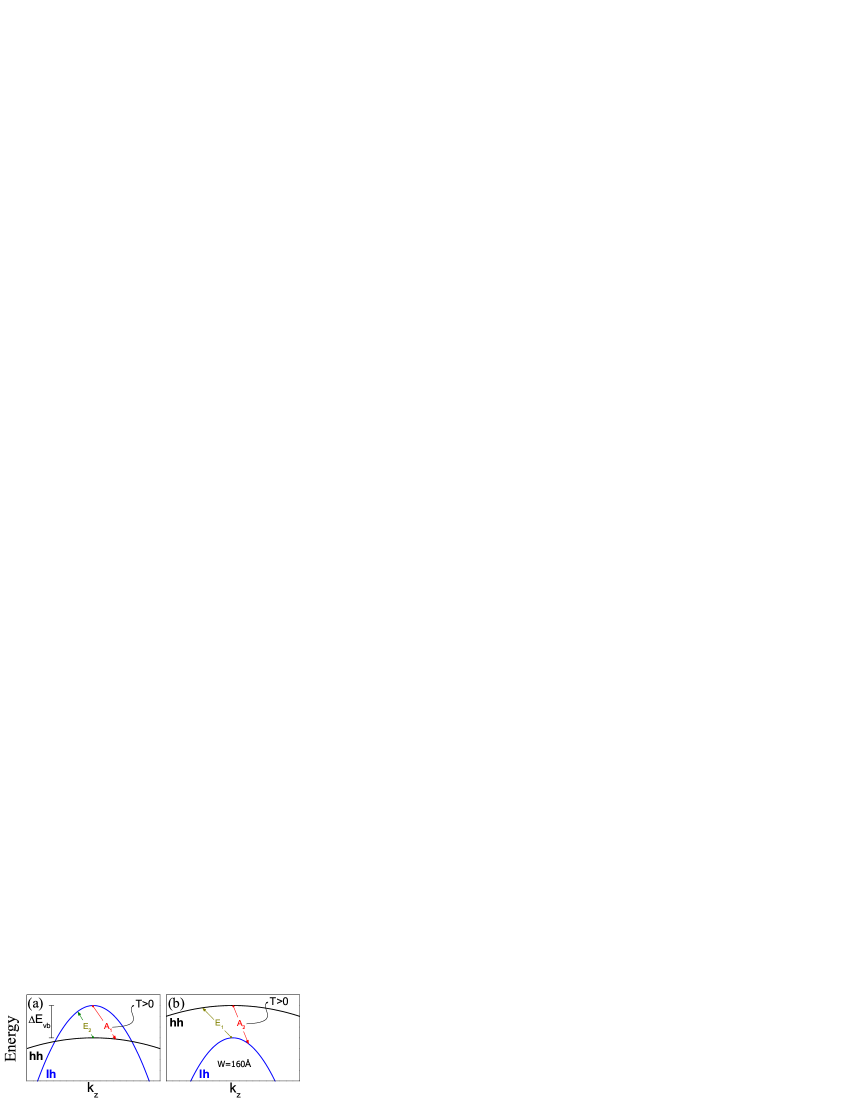
To characterize the initial and final states involved in the scattering processes that affect the mobility, we show in Fig. 2 the relevant valence band structure for two different cases. For thin NWs, with or without strain, the finite NW width leads to a picture similar to Fig. 2(a), where the lh subband is promoted to the top given its higher transverse effective mass, as discussed before. Thus, under such conditions, a hh can be scattered to the subband with lh character through phonon emission (process E1), and at the lh can be excited to the hh subband via phonon absorption (process A1). In the presence of lateral compressive strain, the subbands may switch their relative positions with the hh assuming the top at large NW width. Then, a lh might be scattered via phonon emission (process E2) while a hh can be affected by phonon absorption at (process A2). Notice that by changing the wire radius, one can reach a resonant condition (). On the other hand, with strain, depending on the value of the NW width, the ground state can have a character lh (thin NW) or hh (thick). This behavior is similar for all NW cross sections, as it reflect the transversal quantization.
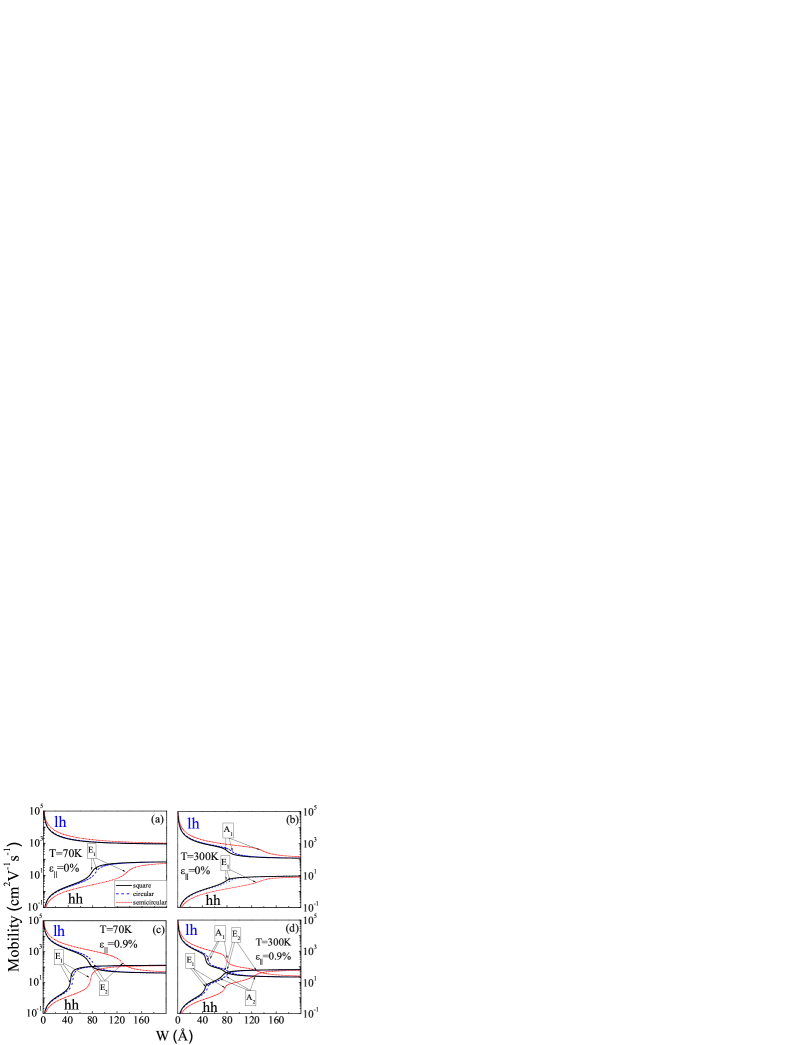
The relative position of the valence subbands is extremely important for the carrier transport in NWs. Given the mobility dependence on the longitudinal effective mass, which modulates the hole-phonon interaction, valence subband shifts may produce sharp fluctuations of the mobility as temperature or structural parameters change. Fig. 3 shows the mobility for different strain and temperature values as function of the NW width. In Figs. 3(a)-(b), the mobility reflects a band configuration similar to the one depicted in Fig. 2(a). At T, in Fig. 3(a), the increase effect of phonon absortion leads to the monotonic decrease of the lh mobility whit increasing NW width, while the hh displays a monotonic mobility increase, as the intersubband separation decreases with increasing NW width. Also, a sharp variation near the region where is seen, the resonant condition greatly enhances LO phonon emission by a hh in panel (a). At higher temperatures, Fig. 3(b), the resonant condition also affects the carriers in the lh subband, producing a sharp drop in mobility (from A1 processes).
Given the band structure modulation with strain, the condition can be attained twice by varying the NW width (corresponding to the cases displayed in Figs. 2(a) and (b)). Thus, two resonant regions appear in Fig. 3(c) where phonons can be emitted by both the hh and lh subbands (E1 an E2 processes, respectively). At higher temperatures, the phonon absorption features appear as additional jumps in the mobility, shown in Fig. 3(d), processes A1 and A2. Notice that the lh and hh subband inversion with increasing NW width, in the presence of strain, is accompanied by crossing of the mobility curves, Figs. 3(c)-(d). Tuning the mobility of a hole system via in-situ changes of the NW width or strain fields, is not an easy task in experiments. As we will see below, however, one can achieve drastic in-situ mobility changes for NWs close to the resonance condition by suitable changes in temperature.
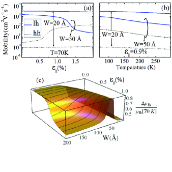
In Fig. 4(a) for a square NW width of , no resonant signatures appear in the strain and temperature range analyzed, while for thicker NWs such conditions become evident for both kind of holes. This situation follows the trends described in Fig. 2, since for thinner NWs, the valence band configuration corresponds to that in Fig. 2(a), with . In turn, by raising the temperature, the process of phonon absorption becomes more effective, reducing the lh mobility at higher temperatures; as displayed in Figs. 4(b). The effect is present for all NWs, although with different features for various values, as we now discuss.
Fig. 4(c) shows the strongly non-monotonic mobility variation with temperature for certain NW widths with energies close to the resonant condition, . This figure shows the lh mobility ratio of high and low temperatures, , where , as function of the NW width for different values of strain. For lh-holes, the mobility at low temperatures is high (Fig. 4(b)) and according to the radius and strain one may observe a drastic drop in mobility at high temperature. For a system with no strain, for example, a large but monotonic drop in the mobility is seen for NWs with large width (larger than ). In real systems, however, free standing NWs grow with built-in strain,nano which has a direct impact on the dependence of on the temperature and width. As the strain increases, the lh-hh subband reversal is possible as the NW width increases, resulting in highly sensitive mobility on temperature and/or width. For example, for , nano and for width values close to mobility exhibit a sharp change in the mobility with temperature.
The authors acknowledge the support of CAPES, CNPQ, FAPESP, NSF, and MWM/CIAM.
References
- (1) H. A. Nilsson, C. Thelander, L. E. Fröberg, J. B. Wagner, L. Samuelson, Applied Physics Letters 89, 163101 (2006).
- (2) X. Duan, Y. Huanh, R. Agarwal, C.M. Lieber, Nature 421, 241 245 (2003).
- (3) G. R. Gray, Semiconductor Laser: Past, Present, and Future(American Intitute of Physics, New York, 1995).
- (4) A. M. Morales, and C. M. Lieber, Science 279, 208 211 (1998).
- (5) X. Duan, and C. M. Lieber, Adv. Mater. 12, 298 302 (2000).
- (6) M. S. Gudiksen, and C. M. Lieber, J. Am. Chem. Soc. 122, 8801 8802 (2000).
- (7) M. T. Bjork, B. J. Ohlsson, et al, Nano Lett. 2, 87 (2002).
- (8) V. Lopez-Richard, J. C. Gonzalez, et al, Nano Letters 9, 3129 (2009).
- (9) L. Villegas-Lelovsky, C. Trallero-Giner, M. Rebello Sousa Dias, V.Lopez-Richard, G. E. Marques, Physical Review B 79, 155306 (2009).
- (10) N. Mori, H. Momose, and C. Hamaguchi, Phys. Rev. B 45, (R)4536 (1992).
- (11) J. Sone, Semicond. Sci. Technol. 7 B210 (1992).
- (12) D. Huang and G. Gumbs, J. Appl. Phys. 107, 103710 (2010).
- (13) Hauser et al., Semicond. Sci. Technol. 9, 951 (1994).
- (14) M. Tsetseri and G. P. Triberis, Phys. Rev. B 69, 075313 (2004).
- (15) S. K. Lyo and D. Huang, Phys. Rev. B 64, 115320 (2001).
- (16) F Murphy-Armando, G. Fagas, and J. C. Greer, Nano Lett. 10, 869-873 (2010).
- (17) M. Rebello Sousa-Dias, Estudo de efeitos qu nticos nas propriedades eletr nicas de nanofios semicondutores, Master’s thesis, Departamento de Física, Universidade Federal de São Carlos (2010).
- (18) V. Lopez, G. E. Marques, J. Drake, C. Trallero-Giner, Phys. Rev. B 56, 15691 (1997).
- (19) Gerald G. Mahan, Many-Particle Physics, 3rd ed. (Kluwer, New York, 2000).
- (20) V. Lopez-Richard, G. E. Marques, C. Trallero-Giner, J. Drake, Phys. Rev. B 58, 16136 (1998).
- (21) Peter Y. Yu and Manuel Cardona, Fundamentals of Semiconductors (Springer, Berlin, 1996).
- (22) J. P. Rino, Y. M. M. Hornos, G. A. Antonio, I. Ebbsjo, R. K. Kalia, and P. Vashishta, J. Chem. Phys. 89, 7542 (1988).
- (23) P. S. Branicio, J. P. Rino, Shimojo F, Applied Physics Letters 88, 161919 (2006).
- (24) P. S. Branicio, J. P. Rino, G. C. Kwan, et al, J. Phys.:Cond. Matter 21, 095002 (2009).
- (25) J. P. Rino,P. S. Branicio, Phys.Status Solid B 244, 239 (2007).
- (26) P. S. Branicio, J. P. Rino, Phys.Status Solid B 244, 331(2007).
- (27) H. Tsuzuki, C. D. Ferreira, M. Rebello Sousa Dias, et al, ACS Nano 5, 5519 (2011)
- (28) InP parameters interaction potential: effective ionic charge Z, electronic polarizability Å3, steric repulsion exponent , van der Waals strength WÅ6, strength of the steric repulsion Åη, three-body strength B, screening lengths for Coulomb Åand charge-dipole interactions Å, two-body cutoff radius Å, three-body range Å, bond angle , and saturation parameter C.
- (29) P. H. Borcherds, G. F. Alfrey, A. D. B. Woods, D. H. Saunderson, J. Phys. C: Solid St. Phys. 8, 2022-30 (1975).
- (30) H. Bilz, W. Kress, Phonon dispersion relations in insulators 107 (Springer series in solid-state sciences)(Springer-Verlag, 1979).
- (31) J. M. Luttinger, Phys. Rev. 102, 1030 (1956).
- (32) F. H Pollak, M. Cardona, Phys. Rev. 172, 816 (1968).
- (33) For deformation potentials, in (dyn cm-2) units, we have and . For elastic modules in (eV) , , and . Landolt ; PRL When used, the mean value of the biaxial strain was . nano
- (34) Landolt-Börnstein Comprehensive Index, ed. O. Madelung and W. Martienssen (Springer, Berlin 1996).
- (35) D. D. Nolte, W. Walukiewicz, and E. E. Haller, Phys. Rev. Lett. 59, 501 (1987).
- (36) A. C. Stotter,Efecto Raman resonante con Campos Magnéticos Intensos en Heteroestructuras Semiconductoras, Phd thesis, Departamento de Física Aplicada, Universidad de Valencia (1993).
- (37) A. Cantarero, C. Trallero-Ginger, and M. Cardona, Phys. Rev. B 39, 8388 (1989).
- (38) , , and . prb3912
- (39) E. D. Grann, K. T. Tsen and D. K. Ferry, Phys. Rev. B 53, 9847 (1996).