Irreversibility and time relaxation in electrostatic doping of oxide interfaces.
Two-dimensional electron gas (2DEG) confined in quantum wells at insulating oxide interfaces Ohtomo:2004p442 have attracted much attention as their electronic properties display a rich physics with various electronics orders such as superconductivity Reyren:2007p214 ; Biscaras:2010p7764 ; Perna and magnetismbert:2011p767 ; li:2011p762 ; brinkman:2007p493 . A particularly exciting features of these hetero-structures lies in the possibility to control their electronic properties by electrostatic gating Caviglia:2008p116 ; biscaras2 , opening up new opportunities for the development of oxide based electronicshwang ; bibes ; Takagi:2010p9802 ; Mannhart:2010p6675 . However, unexplained gating hysteresis and time relaxation of the 2DEG resistivity have been reported in some bias range, raising the question of the precise role of the gate voltage. Here we show that in / and / heterostructures, above a filling threshold, electrons irreversibly escape out of the well. This mechanism, which is directly responsible for the hysteresis and time relaxation, can be entirely described by a simple analytical model derived in this letter. Our results highlight the crucial role of the gate voltage both on the shape and the filling of the quantum well. They also demonstrate that it is possible to achieve a low-carrier density regime in a semiconductor limit, whereas the high-carrier density regime is intrinsically limited.
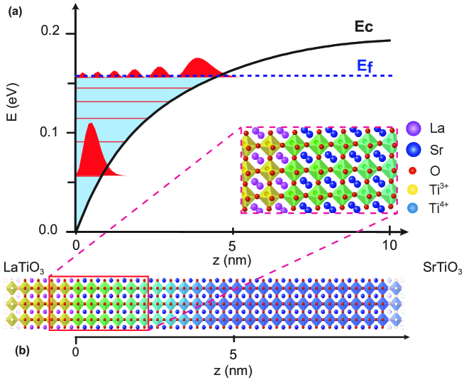
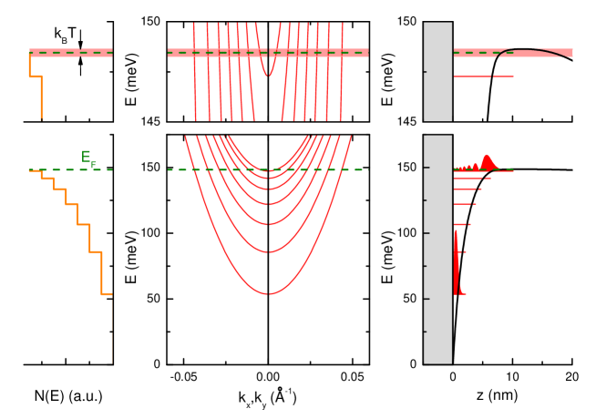
In oxides hetero-structures such as / or / , the bending of the conduction band forms a quantum well at the interface where a 2DEG takes place. Figure 1a shows the numerical simulation of the conduction band profile and sub-bands filling obtained by solving self-consistently Schrödinger-Poisson equations biscaras2 ; Meevasana:2011p9019 . As opposed to semiconducting hetero-structures where the electrons fill only the bottom of the potential well, here, the Fermi energy is intrinsically located near the top of the well. This results from a peculiar situation where the bending of the conduction band is mostly determined by the electron spatial distribution itself. At low temperature, the extension of the gas is of order of 5 nm corresponding to approximatively 12 units cell of (figure 1) basletic ; Copie:2009p5635 . The 2DEG accommodates mainly two types of carriers : the majority low-mobility carriers (LMC) that fill the sub-bands deep in the well and the minority high-mobility carriers (HMC) located in the upper part of the well biscaras2 . The presence of the two types of carriers is only observed below a temperature of approximately 70 K, which corresponds to the range where the dielectric constant of strongly increases when the temperature is lowered and becomes electric field dependentNEVILLE:1972p3397 ; biscaras2 . The LMC are confined close to the interface where is strongly reduced by the electric field, whereas the HMC extend more in where tends to recover its buk value biscaras2 .
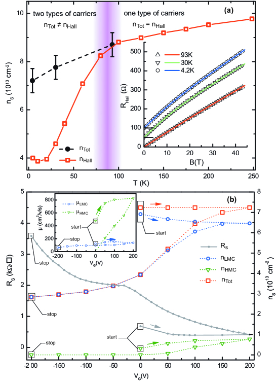
We have studied and epitaxial layers grown on -terminated single crystals by Pulsed Laser Deposition as described in the Supplementary Material section. A metallic back-gate is deposited at the rear of each 0.5 mm thick substrate. The main text of this article focuses mostly on the results obtained on the / heterostructure whereas the data concerning the / heterostructure can be found in the Supplementary Material section. We start by cooling the / heterostructure to 4.2K without applying gate voltage (i. e. un-gated). The evolution of the carrier density with temperature, extracted from Hall effect measured at low magnetic field (7T) is shown in figure 2a. The drastic fall of below 70 K corresponds to the separation of the 2DEG into two types of carriers, as revealed by the observation of a non-linear Hall effect at higher magnetic field (figure 2a inset). The total carrier density shown in figure 2a has been extracted from a two-carrier analysis of the Hall effect that considers carriers with different densities and mobilities (, ) and (, ) biscaras2 ; Ohtsuka:2010p9619 . In the high temperature regime , whereas in the low temperature regime (T70K). The overall decrease of the carrier density from 300K to 4K is due to the trapping of electrons in the defects of .
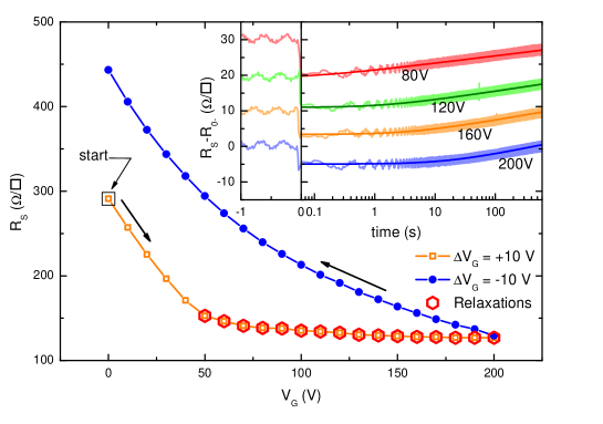
After cooling the sample, the transport properties of the heterostructure are investigated when a positive voltage is applied for the first time on the gate, a situation referred as the first positive polarization. After a small decrease, the resistance of the 2DEG reaches a saturation value that no longer evolves with gate voltage (figure 2b). In a simple Drude picture, such behaviour would indicate that the carrier density remains constant, although, according to electrostatic laws, one expect electrons to be added to the 2DEG. This first polarization is irreversible, since, when the gate voltage is decreased from its maximum value =200 V, the resistance curve deviates from the previous one. Similar behaviour has been mentioned in the literature Bell:2009p6086 ; Reyren:2007p214 . On the same figure, we also plot the evolution of the carrier densities , and = with gate voltage, extracted from a two-carrier analysis of the high field Hall effect. The total number of carriers is found to be rather constant during the first polarization, which is consistent with the saturation of the resistance. The slight decreases of the LMC density is compensated by a slight increase of the HMC one. As already observed in the resistance curve, when the gate voltage is decreased, the total number of carrier does not follow the first polarisation curve.
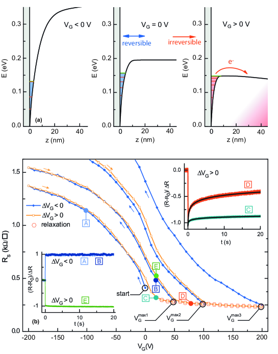
Figure 3a shows the filling of the quantum well for different values of that illustrates the previous experimental observations. The effects of the gate voltage on the interface is twofold : (i) it adds () or removes () electrons to the 2DEG, (ii) it controls the shape of the upper part of the well by tilting the conduction band profile in the substrate. For positive gate voltage, this two effects take place simultaneously to produce HMC as sub-bands are filled near the top of the well, where the band profile becomes shallower. As shown in figure 1a, HMC are also intrinsically present in un-gated hetero-structures during the first cool down, confirming that the Fermi level is located in the upper region of the well. Therefore, when the gate voltage is increased towards positive values, the added electrons rapidly fill the sub-bands all the way up to the top of the well to finally escape in the conduction band of the substrate. Hence, the total carrier density and the resistance of the sample saturate. This behaviour is only possible because the tilting of the conduction band of the has a negative slope away from the interface. The evolution of the carriers mobilities and during the first positive polarisation is consistent with the previous observations (inset figure 2b). Indeed, the mobility of LMC confined deep in the well is found to be rather constant. On the other hand, the mobility of HMC increases rapidly for positive gate voltage before saturating, indicating that the electron added fills the last sub-bands accessible before escaping from the well.
The irreversibility of the first positive polarisation has been investigated in more detail. After cooling down an un-gated sample to 4.2 K, its sheet resistance is measured as a function of gate voltage for different polarization procedures (figure 3b). As opposed to the previous measurements, the first polarisation is made towards negative voltage down to =-200 V. The resistivity increases as expected when electrons are removed from the 2DEG, and no saturation is observed. As the voltage is brought back to =0 V, the resistance curve appears to be fully reversible. However, when the gate voltage is further increased to the positive value of =50 V before being decreased back to =-200 V the curve deviates from the previous one. On the other hand, this new curve is fully reversible as long as the gate voltage is not increased above . The same pattern has been repeated for increasing maximum values of (=100 V, and = 200 V). The same behaviour is also observed in the case of the / sample (supplementary figure 3). These results confirms the scenario proposed previously. The well can be emptied () or filled () reversibly as long as the gate voltage do not increase above a critical value corresponding to the maximum value previously applied to the metallic gate. Beyond this value, the electrons escape irreversibly into the substrate and are lost for the 2DEG. In the literature, a first positive polarisation to the highest voltage value is often used prior to the other measurements to suppress the hysteresis effects Caviglia:2008p116 ; biscaras2 .
The previous experiment raised the question of the escape mechanism of the electrons in the substrate. We performed time resolved resistivity measurements to study the response of the 2DEG to a gate voltage step 10 V. Typical results of these measurements are shown in the insets of figure 3b. When the voltage steps occur in a reversible situation, the resistance shows a clear jump before reaching a stable value, being negative for and positive for (left inset figure 3b). On the contrary, measurements performed in an irreversible situation with a final value of exceeding the previous , display a negative jump of the resistance, before it recovers slowly its original value (right inset figure 3b). At first approximation, this relaxation is logarithmic in time, of the form (figure 3b). In this experiment, the speed of the initial jump in resistance is determined by the characteristic time at which electrons are added to the 2DEG (Supplementary Material).
To analyse the relaxation in the irreversible regime we have developed a model that describes the dynamic of electrons escaping out the well. Details of the calculation are given in the Supplementary Material section. We model the quantum well of figure 1a as a 2D well with an infinite barrier on the side and a barrier of finite height on the side. The total number of electrons in the well right after a gate voltage step is given by where is the number of electrons before the voltage step and is the capacitance per unit of area of the substrate. Assuming that the electrons at the Fermi level can thermally jump across the barrier of energy with a first order kinetics (figure 5a), the Drude resistivity in the relaxation regime is found to be (see Supplementary Material section)
| (1) |
where is the density of states at the Fermi level and ( is the electron mobility). The escape time that appears in equation (1) is given by
| (2) |
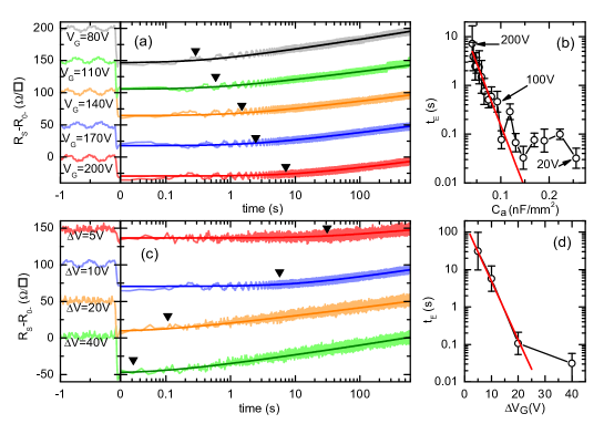
where is the Fermi energy after the voltage step and is a characteristic frequency. A systematic study of the dependence of the relaxation on the polarization parameters has been carried out to validate this model. In particular, we measured the relaxation of the sheet resistance after a step =+10V performed at different values of (figure 4a), and the relaxation of the sheet resistance for different steps values =5, 10, 20, 40V (figure 4c). In both cases, the experimental data are in very good agreement with the theoretical expression (1), confirming that the model catches the essential physics of the phenomena. The same agreement between experiment and theory is also observed for the / sample (supplementary figure 3). To understand the dependence of with and , we can simply express the logarithm of the escape time as
| (3) |
where and are constants whose expressions can be found in Supplementary Material.
For a constant step in the irreversible region, the variation of is consistent with the evolution of the capacitance with gate voltage that can be measured experimentally (figure 4b) biscaras2 . The variation of with is found to be linear for small . For larger , tends to saturate since when the Fermi level has reached the top of the conduction band, electrons are almost directly injected in the conduction band and spill into the substrate.
As already shown in the inset of figure 3b in the limit , the expression (1) reduces to with and . We have verified experimentally that the parameter increases linearly with temperature (figure 5c). This is a direct consequence of a thermally activated mechanism. We emphasise here that the electrons escaping in the conduction band of the substrate are attracted by the positive voltage of the back-gate electrode, but can not reach it. Indeed, the substrate being a thick wide gap insulator, the electron density is too small to create a metallic state. Therefore, electrons diffuse in the substrate until they get trapped in the defects of the crystal. Hence, these electrons do not contribute to electronic transport, but do play a role to maintain the polarisation between the two sides of the substrate. Figure 5b shows that the trapped electrons can be released in the 2DEG if the temperature of the sample is increased above two characteristic values 70K and 170 K in the case of the / sample.
In summary, we have shown that in / and / interfaces, the Fermi level is instrinsically close to the top of the quantum well created by the bending of the conduction band at the interface. When the carrier density is increased by an electrostatic back-gate voltage beyond a critical value, most of the added electrons escape in the substrate conduction band at a rate well explained by a thermally activated leaking out of the well. This phenomenon which appears to be common to all based interfaces, is directly responsible for the saturation of the 2DEG properties with gate voltage such as the mobility and the carrier density but also the superconducting transition temperature observed at lower temperature (supplementary figure 4). It also certainly affects the strength of Rashba spin-orbit coupling that was shown to increase strongly in the region of positive gate voltage caviglia2 . Hence, these results put a limitation on the performances achievable with back gated heterostructures, in particular in terms of high-mobility and Rashba spin-orbit, two important properties that originally contributed to the emergence of based interface, as they open future perspectives in the field of oxides electronics. To overcome this problem we suggest to realise double gated structures. A back gate could be used to engineer the shape of the quantum well that determines the mobility of carriers through the bending of the conduction band. Independently, electrons could be added into the well thanks to a top gate.
The Authors gratefully thank M. Grilli, S. Caprara and A. Millis for stimulating discussions. This work has been supported by the Région Ile-de-France in the framework of CNano IdF and Sesame program. Part of this work has been supported by Euromagnet II. The work at IIT Kanpur has been funded by the Department of Information Technology. RCB acknowledge the J C Bose Fellowship of the Department of Science and Technology, Government of India
References
- (1) Ohtomo, A., Hwang, H. Y., A high-mobility electron gas at the / heterointerface Nature 427, 423-426 (2004).
- (2) Reyren, N., Thiel, S., Caviglia, A. D., Kourkoutis, L. F., Hammerl, G., Richter, C., Schneider, C. W., Kopp, T., Ruetschi, A.-S., Jaccard, D., Gabay, M., Muller, D. A., Triscone, J.-M., Mannhart, J., Superconducting interfaces between insulating oxides, Science 317, 1196-1199 (2007).
- (3) Perna, P., Maccariello, D., Radovic, M., di Uccio, U. S., Pallecchi, I (Pallecchi, I., Codda, M., Marre, D., Cantoni, C., Gazquez, J., Varela, M., Pennycook, S. J., Granozio, F. Miletto, Conducting interfaces between band insulating oxides: The / heterostructure, Appl. Phys. Lett. 97, 152111 (2010).
- (4) Biscaras, J., Bergeal, N., Kushwaha, A., Wolf, T., Rastogi, A., Budhani, R. C., Lesueur, J., Two-dimensional superconductivity at a Mott insulator/band insulator interface /, Nature Communications 1, 89 (2010).
- (5) Bert, J. A., Kalisky, B., Bell, C., Kim, M., Hikita, Y., Hwang, H. Y., Moler, K. A., Direct imaging of the coexistence of ferromagnetism and superconductivity at the / interface, Nature Phys. 7, 767-771 (2011).
- (6) Li, L., Richter, C., Mannhart, J., Ashoori, R. C., Coexistence of magnetic order and two-dimensional superconductivity at / interfaces, Nature Phys. 7, 762 766 (2011).
- (7) Brinkman, A., Huijben, M., Van Zalk, M., Huijben, J., Zeitler, U., Maan, J. C., Van der Wiel, W. G., Rijnders, G., Blank, D. H. A., Hilgenkamp, H., Magnetic effects at the interface between non-magnetic oxides, Nature Mater. 6, 493-496 (2007).
- (8) Caviglia, A. D., Gariglio, S., Reyren, N., Jaccard, D., Schneider, T., Gabay, M., Thiel, S., Hammerl, G., Mannhart, J., Triscone, J. -M., Electric field control of the / interface ground state, Nature 456, 624 (2008).
- (9) Biscaras, J., Bergeal, N., Hurand, S., Grossetete, C., Rastogi, A., Budhani, R. C., LeBoeuf, D., Proust, C., Lesueur, J., Two-dimensional superconductivity induced by high-mobility carrier doping in / hetero-structures, Phys. Rev. Lett. (in press) arXiv:1112.2633 (2012).
- (10) Bibes, M. Villegas, J. E. and Barth l my, A. Ultrathin oxide films and interfaces for electronics and spintronics, Adv. Phys., 60, 5-84 (2011).
- (11) Takagi, H., Hwang, H. Y. An Emergent Change of Phase for Electronics Science 327, 1601-1602 (2010).
- (12) Mannhart, J., Schlom, D. G., Oxide Interfaces-An Opportunity for Electronics, Science 327, 1607-1611 (2010).
- (13) Hwang, H. Y., Iwasa, Y., Kawasaki, M., Keimer, B., Nagaosa, N. and Tokura, Y. Emergent phenomena at oxide interfaces, Nature Materials, 11, 103-113 (2012).
- (14) Meevasana, W., King, P. D. C., He, R. H., Mo, S-K., Hashimoto, M., Tamai, A., Songsiriritthigul, P., Baumberger, F., Shen, Z-X., Creation and control of a two-dimensional electron liquid at the bare surface, Nature Mater. 10, 114–118 (2011).
- (15) Basletic, M., Maurice, J. -L., Carretero, C., Herranz, G., Copie, O., Bibes, M., Jacquet, E., Bouzehouane, K., Fusil, S., Barthelemy, A., Mapping the spatial distribution of charge carriers in / heterostructures, Nature Materials, 7, 621-625 (2008).
- (16) Copie, O., Garcia, V., Boedefeld, C., Carretero, C., Bibes, M., Herranz, G., Jacquet, E., Maurice, J. -L., Vinter, B., Fusil, S., Bouzehouane, K., Jaffres, H., Barthelemy, A., Towards Two-Dimensional Metallic Behavior at / Interfaces, Phys. Rev. Lett. 102, 216804 (2009).
- (17) Neville, R., Mead, C., Hoeneise, B., Permitivity of strontium-titanate, J. Appl. Phys. 43, 2124–2131 (1972).
- (18) Ohtsuka, R. Matvejeff, M., Nishio, N., Takahashi, R., Lippmaa, M., Transport properties of / heterostructures, Appl. Phys. Lett. 96, 192111 (2010).
- (19) Bell, C., Harashima, S., Kozuka, Y., Kim, M., Kim, B. G., Hikita, Y., Hwang, H.Y., Dominant Mobility Modulation by the Electric Field Effect at the / Interface Phys. Rev. Lett. 103, 226802 (2009).
- (20) Caviglia, A.D., Gabay, M., Gariglio, S., Reyren, Cancellieri, C., Triscone, Tunable Rashba Spin-Orbit Interaction at Oxide Interfaces Phys. Rev. Lett. 104, 126803 (2010).
- (21) G. Koster et al. Appl. Phys. Lett.,73, 2920 (1998).
- (22) C. Canciellieri, Europhys. Lett. 91, 1704 (2010).

Supplementary Material
1. Growth of the heterostructures
/ hetero-structures were grown at ITT Kanpur (India) using
excimer laser based PLD on commercially available (Crystak gmbh Germany) single crystal substrates of
(100) oriented. The substrates were given a buffered HF treatment to expose terminated
surface. Before deposition, they were heated in oxygen pressure of 200 mTorr in the temperature range of 850 to 950 C∘ for one hour
to realize surface reconstruction. The source of is a stoichiometric
sintered target of 22 mm in diameter which was ablated in oxygen partial
pressure of Torr with energy fluence of 1 J/cm2 per pulse
at a repetition rate of 3 Hz to acheive a gowth rate of 0.12 Å/s. Under these conditions, the phase is grown on substrates, as shown by X-Rays diffraction patterns Biscaras:2010p7764 . In this study, we used 15 u.c. thick layers on 0.5 mm thick substrates.
/heterostructures were fabricated at UMR CNRS/Thales (Paris, France). A thin film is deposited by PLD (Surface PLD system) on a -terminated -oriented substrate (Crystec and SurfaceNet). A buffered HF treatment followed by annealing, as described in Ref. Koster , was used to obtain the termination required to obtain the conducting electronic system at the interface. The KrF excimer (248 nm) laser ablates the single-crystalline target at 1 Hz, with a fluence between 0.6 and 1.2 J/cm2 in an O2 pressure of mbar. The substrate is typically kept at 730C∘ during the growth, which is monitored in real-time by RHEED. As the growth occurs layer-by-layer, it allows us to control the thickness at the unit cell level. After the growth of the film, the sample is cooled down to 500C in mbar of O2, where the oxygen pressure is increased up to 400 mbar. In order to reduce as much as possible the presence of oxygen vacancies (in both the substrate and the film), the sample stays in these conditions for 30 minutes before being cooled down to room temperature Cancellieri2010 . The substrate-target distance is about 57 mm, leading to a growth rate of about 0.2 Å/s in the above conditions. In this study, we used 5 u.c. thick layers on 0.5 mm thick substrates.
1. Characteristic charging time of the sample
The 2DEG carrier density at the interface can be electrostatically tuned by a metallic gate deposited at the back of the substrate. The heterostructure forms a capacitor, whose plates consist of the metallic gate on one side and the 2DEG on the other side, and whose dielectric material is the substrate.
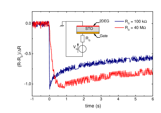
As shown by the scheme in Figure 6, the heterostructure of capacitance is placed in serial with an external resistor of resistance defining a simple RC circuit. Therefore, the change in the charge density of the 2DEG after a voltage step is not instantaneous, but reach it’s final value with a time dependence where . In a simple Drude model, the resistance of the 2DEG after a voltage step is expected to evolve with the same time dependence. Figure 6 show the resistance of the 2DEG as a function of time, upon applying a voltage step 10 V, for two different values of the external resistance. The blue curve corresponds to the short time (100 k) used for all the experiments reported in the main text. It shows a sharp decrease of resistivity, followed by the logarithmic relaxation discussed in the main text. On the other hand, the red curve corresponds to a longer time (40 M) and shows that the initial decrease of the resistance is much slower. However, the logarithmic relaxation remains basically unchanged. We thus see that in our experiment the time at which the electrons are added to the 2DEG do not interfere with the thermal leaking of electrons into the substrate.
2. Thermal escape of electrons from the quantum well
We have built a model to account for the relaxation of resistivity in the irreversible regime based on the thermal escape of the electrons over the top of the conduction band profile at positive gate voltage. The band bending and sub-bands energies of the / interface in the irreversible regime are shown in Figure 7 as an illustration biscaras2 . However, this model is very general and does not depend on the details of the well such as its shape.
We consider a 2D potential well with a finite barrier height and a finite number of parabolic sub-bands of energy (=1,…,). We assume that electrons at the Fermi level can thermally jump over the barrier with a first order kinetics :
| (4) |
where is the density of electrons in the well and is the kinetic factor. For thermally activated hoping the latter follows an Arrhénius law : where the activation energy is , and is a characteristic frequency factor. Hence, considering that the density of state of a 2D sub-band is constant and that the Fermi level always stay above the highest sub-band level (the well is almost totally filled up), the equation on is :
| (5) |
which is equivalent to a problem with only one level but with a density of state multiplied by . Considering low temperatures (), the variations of can be neglected in at first order, which gives the solution :
| (6) |
where is the Fermi level at =0 (in our case : just after the voltage step) and is the characteristic escape time :
| (7) |
where is the total density of state at the Fermi level.
It follows that the Fermi level is constant for and then decreases logarithmically at longer time. Hence, the conductivity calculated from a simple Drude model with a constant mobility (small variation of ) is given by
| (8) |
The pre-factor of the logarithm is of the order of cm-2, which is sufficiently small compared to the density of electrons to allow for a first order approximation in the resistivity :
| (9) |
where is the Drude resistivity just after the step. As shown in the main text, this time dependence of the resistance fits the experimental data with a very good accuracy, and the logarithm pre-factor shows experimentally the thermal activation of the process.
To analyse the experimental behaviour of the escape time with gate voltage, we now consider a positive gate voltage step at . Starting from a density of electrons , the density after the step is :
| (10) |
where is the capacitance per unit area of the sample. One assumption made here is that there is enough “space” in the well to receive all the added electrons at initial time (which is true for small ). For small , the variations of with can be neglected, such that the Fermi level rises up according to :
| (11) |
Hence, when replaced in equation (7), the variation of with and is given by:
| (12) |
where and .
As shown in figure 4 of the main text, the variations of follow a linear dependence with both for 100 V (deep irreversible regime), and (for values lower than 40 V) at +200 V for instance.
3. Relaxation results on / interface
Similar time resolved resistance measurement were carried on a 5 unit cell grown on -terminated substrate. As for the / heterostructures, measurements at low temperature with different polarisation procedures show that negative first polarisations are reversible, while the positive first polarisations are irreversible. Supplementary Figure 3 shows the resistivity saturation upon the first positive polarisation and the associated thermal escape of the electrons, which is well fitted by our model.
At lower temperature, the superconducting also saturates during the first positive polarisation (Fig. 9). This is a further indication that indeed all the electronic properties of the 2DEG follow this behavior. This observation is also consistent with the fact that superconductivity is intimately related to High Mobility Carriers (HMC) which set at the edge of the quantum well biscaras2 . Indeed, when the un-gated hetero-structure is cooled down, there are spontaneously HMC at the top of the quantum well that induces superconductivity in the 2DEG. During the electrostatic forming, HMC density is roughly constant (see main text Figure 2b), and so is .
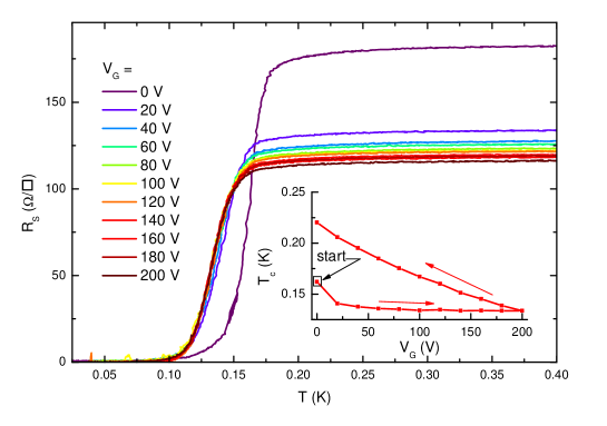

Fig. 10 shows the warm-up curve at =0 V after a positive polarisation deep in the irreversible regime. As the temperature is increased, electrons are de-trapped and return to the 2DEG. However, the resistivity steps are less clear than in the / system and shows numerous release temperatures with various amplitudes : 70 K (almost invisible), 130 K, 170 K, 210 K and 280 K. The 2DEG goes back to its original state only a high temperature (280 K). The origin of these temperatures and their differences with the / heterostructure are unknown at the moment.