Diffusion-Emission Theory of Photon Enhanced Thermionic Emission Solar Energy Harvesters
Abstract
Numerical and semi-analytical models are presented for photon-enhanced-thermionic-emission (PETE) devices. The models take diffusion of electrons, inhomogeneous photogeneration, and bulk and surface recombination into account. The efficiencies of PETE devices with silicon cathodes are calculated. Our model predicts significantly different electron affinity and temperature dependence for the device than the earlier model based on a rate-equation description of the cathode. We show that surface recombination can reduce the efficiency below 10 % at the cathode temperature of 800 K and the concentration of 1000 suns, but operating the device at high injection levels can increase the efficiency to 15 %.
I Introduction
Currently solar energy is converted to electric power using two technologies: photovoltaic (PV) solar cells and concentrated solar power systems based on heat engines book:Kalogirou . The former system requires low and the latter high operating temperatures. This discrepancy poses a challenge for combination of the two systems in tandem, where the heat engines exploit the waste heat of the PV system. A photon-enhanced-thermionic-emission (PETE) device proposed by Schwede et al. art:Schwede is a PV device which benefits from high operation temperatures. It can be coupled to a heat engine, thereby allowing total efficiencies above 50% to be potentially reached.
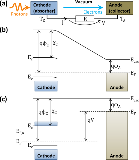
The PETE device is depicted in Fig. 1. The photons are absorbed in the cathode, i.e. the absorber, which is a P-type semiconductor. The cathode material should have a suitably low energy gap so that most of the solar photons are absorbed. The absorbed photons are themionically emitted from the cathode to vacuum, where they travel to the anode, i.e. the electron collector. The surface of the cathode should have a low electron affinity in order to have reasonably strong thermionic emission. Electron affinity can be tuned significantly below the bulk value by different surface coatings (see Refs. art:Schwede, ; art:Guo, and references therein). Even negative electron affinities can be obtained for silicon art:Guo . These coatings, however, might not be stable at the high operation temperatures of PETE devices. The anode material can be metal or N-type semiconductor with suitably low work function in order to have high output voltage for the device.
In the PETE device model of Ref. art:Schwede, the cathode material is described by a single rate equation that neglects many important effects, such as diffusion and realistic recombination. In this article, we present a model that takes the most of the relevant effects in semiconductors into account. We solve the electron density in the cathode numerically in the general case and derive also a semi-analytical model, which can be used at low injection levels. Silicon is a good candidate for PETE due to its rather low band gap, good thermal stability, high availability, cost-efficiency, and good manufacturability. Therefore, we use our models to calculate the characteristics of a PETE device with a silicon cathode using experimentally verified material data. We find that at low temperatures our model predicts a significantly lower efficiency than the model presented in Ref. art:Schwede, . The overall temperature and electron affinity dependency of the efficiency differs also from that of Ref. art:Schwede, . Furthermore, we show that surface recombination can reduce the efficiency of the PETE device below 10 %, but operating the device at high injection levels can provide an enhancement where efficiency of 15 % is reached.
II Theory
II.1 Semiconductor material model
The Fermi level is solved numerically using the electroneutrality condition book:Sze , where and are the densities of electrons and holes in the thermodynamical equilibrium, and and are the densities of ionized acceptors and donors, respectively. For the temperature dependence of the band gap of silicon we use the standard formula book:Sze
| (1) |
where eV, eVK, and K.
The total minority-electron lifetime in bulk can be written as art:Altermatt_rev ; book:Schroder ; art:Altermatt
| (2) |
where is the radiative recombination coefficient, and are the densities of electrons and holes, respectively, and are the Auger recombination coefficients for electrons and holes, respectively, and is the Shockley-Read-Hall (SRH) recombination lifetime, which is directly proportional to the density of the deep-level impurities in the material, and it increases when the injection level is increased book:Schroder . The SRH lifetime has constant saturation values both in low and high injection regimes book:Schroder . Therefore, we use constant s to represent a high quality silicon art:Altermatt at either low or high injection level. For silicon book:Schroder cms and cms, which is a value measured at low injection level. In a P-type material determines the Auger lifetime in low and the ambipolar Auger coefficient in high injection conditions book:Schroder , respectively. The experimental high-injection value for differs from measured at low injection levels art:Altermatt ; art:Altermatt_rev . We take the both injection regimes into account using an artificial value of cms for . For electron mobility in silicon we use a model art:Reggiani optimized for a wide temperature range. Mobility is linked to the diffusion coefficient , where is the absolute temperature and the elementary charge. For the absorption coefficient of silicon we use a widely-used semi-empirical model art:Rajkanan ; book:Green .
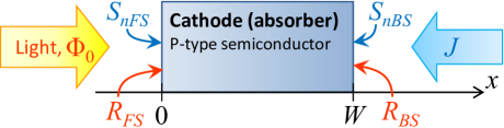
II.2 Electron density
The electron density in the cathode sketched in Fig. 2 can be calculated using the continuity equation, the generation and recombination rate equations, and the drift–diffusion current formulas for the charge carriers book:Sze . We assume that the electric field inside the cathode is approximately zero, because the most of the voltage difference is across the vacuum gap and the photogeneration of electron-hole pairs supports the local approximate charge neutrality. This simplifies the solution considerably, since holes need not to be taken into account explicitly. In addition, the band bending near the cathode surface (see Fig. 1b) is neglected, since the effect is small and the PETE device is mostly operated near the flat-band case (shown in Fig. 1c), where the band bending disappears. The excess-electron density can be described by
| (3) |
where is the diffusion length of electrons and the generation is given by
| (4) |
where is the absorption coefficient, is the incident flux of photons, is the front (back) surface reflection coefficient, and is the thickness of the cathode. The boundary conditions are
| (5) | ||||
| (6) |
where is the front (back) surface recombination velocity and is the density of the output current.
The analytical solution exist when is constant, which is valid at low injection levels (i.e. ). Assuming the low-injection case and using Eqs. (5) and (6) the solution of Eq. (3) at is given by
| (7) |
where
| (8) | ||||
| (9) | ||||
| (10) |
and
| (11) |
where is the wavelength of photons. The first term in Eq. (7) describes the fact that the electrons need to diffuse from bulk of the cathode to the back surface in order to be emitted. When current is drawn, will decrease because of this diffusion process. The second term in Eq. (7) represents the excess electrons due to the photogeneration.
II.3 Output current
The density of the cathode current, which corresponds to electrons emitted from the cathode, can be written using the quasi Fermi level as
| (12) |
where when , and , when , is Richardson’s constant, and is the absolute temperature of the cathode. The flat-band voltage is defined as
| (13) |
where is the work function of the anode material and
| (14) |
is the work function and the electron affinity of the cathode material. The density of the anode current, which corresponds to electrons emitted from the anode, is given by
| (15) |
where when , and , when , is Richardson’s constant of the anode, and is the absolute temperature of the anode. We assume that all the electrons emitted from the cathode are collected by the anode and vice versa:
| (16) |
The flat band voltage is an important parameter for the efficiency of the PETE device. At voltages above the additional energy barrier for the electrons emitting from the cathode appears (see Eq. (12)). This decreases considerably. At voltages below the electrons emitted from the anode are hindered by the energy barrier (see Eq. (15)). This allows to be reduced by lowering . In general, the highest output power will often be obtained near . However, when , the high thermal energy of the cathode electrons allows the range to be used as well.
Using and Eqs. (7) and (12)–(16) the output electric current density can be written alternatively as
| (17) |
where the photocurrent is given by
| (18) |
where
| (19) |
The dark current is given by
| (20) |
where when , and , when . The dark current is the electric current that flows through the device when there is no illumination. Under illumination it usually decreases the total current, thus it should be eliminated. This can be done by choosing optimally. However, if is very low, the direction of can change, and the device harvests energy also from the thermal energy of cathode electrons similarly as a thermionic converter.
III Results and discussion
The semi-analytical model, Eqs. (8), (11), and (17)–(20), applies in the low injection condition () with a P-type cathode material () book:Schroder . The numerical calculations were performed using Eqs. (3)–(6) and (12)–(16). In both models was optimized numerically for maximum output power. The AM1.5 direct+circumsolar spectrum applicable to solar concentrators was used in the calculations. We use ⟨111⟩ silicon as the cathode surface, for which book:Sze AcmK2. For the material parameters of the anode we use the same values as Schwede et al. art:Schwede , V and AcmK2. was set at 573.15 K in order the heat engine potentially coupled to the anode to have a reasonably high efficiency art:NH3_H20_Rankine ; art:Solar_polygeneration . We also assume and for simplicity. The effect of , however, is not very large (see below), since it has an effect only on the absorption of low energy photons.
The efficiencies of PETE devices with various values of are plotted as functions of in Fig. 3. They increase with increasing and decreasing due to the increase of . Using instead reduces the efficiency from 13.0 % to 11.7 % at 550 K in the case .
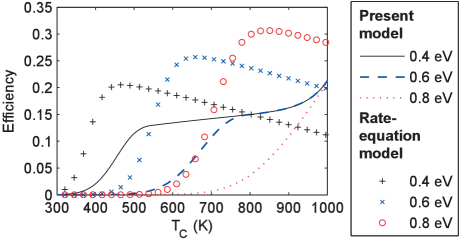
Fig. 3 shows also the efficiencies given by the simple rate-equation model art:Schwede , which assumes that all photons with energy greater than are uniformly absorbed in the cathode. Only the uniform radiative recombination is taken into account with a general model based on the black-body radiation. At low the rate-equation model suggests much higher efficiencies than the present more complete model. This is mostly due to the facts that all the possible photons are absorbed and the Auger recombination is not included in the rate-equation model.
The efficiency is a balance between many opposing effects, which depend on and : Increasing increases which increases the efficiency. On the other hand, high reduces the efficiency due to the Auger recombination which is proportional to . The effect of the bulk recombination can be reduced by decreasing , but then some of the photons will not be absorbed. Although 5 m is already small thickness for a silicon absorber, but, if is increased to 50 m while keeping constant, the efficiency reduces from 13.0 % to 8.4 % at 550 K in the case eV. At high the efficiency curves of the present model unite regardless of the differences in . The reason for this is that the total current does not depend on in this range: When the range can be utilized and the output current density can be written using Eqs. (12)–(16) as expexp. The rate-equation model does not behave like this at high , because decreases much faster with increasing than in the present model. This is caused mostly by the differences in the modeling of recombination and the narrowing of the band gap with increasing which is taken into account only in the present model. The latter effect enhances both photogeneration and thermal generation of electrons, which causes the apparent efficiency increase at K.
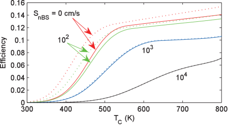
The effect of on the efficiency of the PETE device is shown in Fig. 4: Even a low value of reduces the efficiency remarkably. Similar results were also obtained with various values of . The efficiency is more sensitive to than because photogeneration is much stronger near the front surface than near the back surface. The semi-analytical model is in a very good agreement with the numerical model when the recombination velocities are cm/s since the injection level is below 0.1 at K. In the low-injection conditions achieving surface recombination velocities less than 100 cm/s requires usually use of back surface field structures book:Sze . However, the surface recombination velocity decreases rapidly when the injection level is increased book:Sze and values below 2 cm/s can easily be reached at injection level of unity (details depend on the properties of the surface states) book:Schroder . Therefore, the case of zero surface recombination can actually be realistic for a PETE device.
IV Conclusions
In summary, we have built a theoretical model for PETE devices. Our model takes electron diffusion, inhomogeneous photogeneration, and bulk and surface recombination into account. In comparison to the rate equation model of Ref. art:Schwede, our model predicts different dependency of efficiency on such paramaters as cathode electron affinity and temperature. In most cases our model also predicts lower efficiency. Especially, the surface recombination present on real surfaces can reduce the efficiency to extremely low values. However, the surface recombination might have only a very weak effect on the performance, since the PETE device works often in the high-injection conditions where the surface recombination can be rather small book:Schroder . We finally point out that the realization of the PETE device requires choices of many parameter values and materials which should all be optimized. In addition, the heat balance between the PETE device and the heat engine coupled to the anode, which was not considered in this article, should be managed as well. Full optimization with heat balance modelling will be left for future studies.
Acknowledgements.
Fruitful discussions with J. Tervo, J. Ahopelto, K. Reck, O. Hansen, and P. Kuivalainen are gratefully acknowledged. This work has been financially supported by Nordic Energy Research (project HEISEC) and by the Academy of Finland (grant nr. 252598).References
- (1) S. A. Kalogirou, Solar Energy Engineering – Processes and Systems (Elsevier, New York, USA, 2009).
- (2) J. W. Schwede, I. Bargatin, D. C. Riley, B. E. Hardin, S. J. Rosenthal, Y. Sun, F. Schmitt, P. Pianetta, R. T. Howe, Z.-X. Shen, and N. A. Melosh, Nature Materials 9, 762 (2010).
- (3) S. M. Sze, Physics of Semiconductor Devices, 2nd ed. (Wiley-Interscience, New York, USA, 1981).
- (4) P. P. Altermatt, J. Comput. Electron. 10, 314 (2011).
- (5) D. K. Schroder, Semiconductor material and device characterization, 3rd ed. (Wiley-Interscience, Hoboken, USA, 2006).
- (6) P. P. Altermatt, J. Schmidt, G. Heiser, and A. G. Aberle, J. Appl. Phys. 82, 4938 (1997).
- (7) S. Reggiani, M. Valdinoci, L. Colalongo, M. Rudan, and G. Baccarani, VLSI Design 10, 467 (2000).
- (8) K. Rajkanan, R. Singh, and J. Shewchun, Solid-State Electron. 22, 793 (1979).
- (9) M. A. Green, Solar Cells – Operating Principles, Technology and System Applications (The University of South Wales, Kensington, NSW, Australia, 1982).
- (10) W. R. Wagar, C. Zamfirescu, and I. Dincer, Energy Conv. Management 51, 2501 (2010).
- (11) A. Kribus and G. Mittelman, J. Solar Energy Eng. 130, 011001 (2008).
- (12) T. Guo, J. Appl. Phys. 72, 4384 (1992).