Tunable single-photon heat conduction in electrical circuits
Abstract
We build on the study of single-photon heat conduction in electronic circuits taking into account the back-action of the superconductor–insulator–normal-metal thermometers. In addition, we show that placing capacitors, resistors, and superconducting quantum interference devices (SQUIDs) into a microwave cavity can severely distort the spatial current profile which, in general, should be accounted for in circuit design. The introduction of SQUIDs also allows for in situ tuning of the photonic power transfer which could be utilized in experiments on superconducting quantum bits.
I Introduction
In the past decade great progress has been achieved in the fields of circuit quantum electrodynamics (Blais et al., 2004; Wallraff et al., 2004; Blais et al., 2007; Deppe et al., 2008; Fink et al., 2008; Mariantoni et al., 2011a; Paik et al., 2011; Niemczyk et al., 2010) and photonic heat conduction (Meschke et al., 2006; Ojanen and Heikkilä, 2007; Schmidt et al., 2004; Pascal et al., 2011; Muhonen et al., 2012). The first attempts to combine them by studying single-photon heat conduction in a microwave cavity were recently reported in Ref. Jones et al., 2012. This approach has the potential to deliver practical benefits, both for investigating fundamental quantum phenomena and in order to deliver the practical tools needed in the field of superconducting quantum computing where the manipulation of microwave photons is becoming increasingly importantHouck et al. (2007); Hofheinz et al. (2008, 2009); Schuster et al. (2007); Bozyigit et al. (2011); Chen et al. (2011).
In Ref. Jones et al., 2012, a model to study single photons in a well-defined environment was introduced. The practical setup proposed allows for heat exchange between two normal-metal resistors in a superconducting cavity, for which the photonic heat conduction dominates. This scheme involves a pair of superconductor–insulator–normal-metal (SIN) tunnel junctions Giazotto et al. (2006) to control the temperature of one of the resistors, enabling remote heating or cooling of low-temperature circuit elements. The coupling of the resistors to the superconducting cavity also allows them to act as engineered and controllable environments for the cavity modes. In practice, controlling and measuring the temperatures of the resistors inevitably introduces additional power sources for the electron clouds in the resistors. Additionally, there may also be heat transfer between the resistors by quasiparticle excitations in the superconductor. In this paper, we extend the analysis of the system in Ref. Jones et al., 2012 by accounting for the SIN junctions and quasiparticle power sources and show that the observation of single-photon heating and cooling is still experimentally feasible. In addition, this more comprehensive model allows us to impose a cutoff-temperature below which cooling is not observable.
In the second half of this paper, we return to the classical transmission line frameworkPascal et al. (2011); Jones et al. (2012) in order to investigate how placing capacitors, resistors, and superconducting quantum interference devices (SQUIDs) into the transmission line affects the photon mode profile. We show that the distortion of the photon modes responsible for heat transport can be dramatic, and should potentially be accounted for in typical circuit design. Furthermore, this mode distortion suggests a resolution to the discrepancy between the power transfer calculated with the quantum and classical models in the strong coupling limit, which was observed in Ref. Jones et al., 2012. Since many future cavity photon experimentsMariantoni et al. (2011b) will utilize two or more cavities, e.g., for filtering or isolating modes, we also focus on the effect of placing a capacitive break into the central superconducting strip of the transmission line.
We study the possibility of using SQUIDs for in situ tuning of the single-photon power in a cavity. We further develop the classical transmission line model, and demonstrate that such tuning is indeed possible and can be rather effective. In the experiment of Ref. Meschke et al., 2006, in situ tuning of photonic heat conduction was demonstrated experimentally by using SQUIDs to vary the impedance of the connecting circuit. However, no cavity was present and hence a lumped element model for the impedance was sufficient. In superconducting quantum computing, SQUIDs are often placed into a cavity in order to create or readout quantum bits, qubitsYang et al. (2003); Zhou et al. (2002); Chiorescu et al. (2004). Introducing SQUIDs into the line also provides some control over the eigenfrequencies of the photons in the cavity so that they may be, e.g, tuned in and out of resonance with a qubit. This tuning has been demonstrated experimentally through two approaches: either the SQUIDs terminate the transmission line, thus giving variable boundary conditions Castellanos-Beltrana and Lehnert (2007); Sandberg et al. (2008); Wilson et al. (2011); Zakka-Bajjani et al. (2011), or they are placed in the center conductor of the linePalacios-Laloy et al. (2008). In Ref. Wilson et al., 2011, the dynamical Casimir effect was demonstrated; photons were created in a SQUID-terminated transmission line by rapid variation of the SQUID flux. Tunable resonators are also required in several other practical applications: in Ref. Zakka-Bajjani et al., 2011, two photon number states are held in a cavity at different frequencies allowing for a parametric interaction between them.
This paper is outlined as follows. In Sec. II, we review the basic theory required to calculate the heat power between two normal-metal islands in the center conductor of the line and the theory of the SIN junctions needed to measure their temperature. We also discuss the heat power due to quasiparticles between two such islands into the model. We then study the remote heating and cooling in the presence of SIN junctions in Sec. III. Section IV gives a brief discussion of the discrete transmission line model and the mode profiles are solved with a capacitor placed into the line. In Sec. V, the model is expanded to include resistors and the power transfer between them is calculated. In Sec. VI, we analyze the case of SQUIDs in the line by demonstrating the in-situ tuning of the cavity eigenfrequencies and power transfer.
II Comparison of the thermal power sources
II.1 Phononic and cavity photonic power
In Ref. Jones et al., 2012, the heat exchange between two normal-metal resistors in a superconducting cavity was studied in a setup similar to Fig. 1 with no SQUID or capacitor in the line, i.e., and .
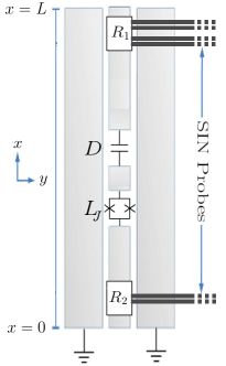
The equilibrium temperature of the second resistor, , was calculated when the temperature of the first resistor, , was held constant. Power from only two sources was included: the coupling between the electrons in a resistor with the phonons at the bath temperature , , and photon exchange between the resistors and the cavity, . The latter can be derived in the weak coupling limit where the Hamiltonian for a single resistor in a cavity, at position , may be expressed as
| (1) |
where is the total voltage fluctuation across the resistor and is the integral of the charge density in the cavity from to . Since the coupling between the resistor and the cavity is linear, applying Fermi’s golden rule with this Hamiltonian yields a photonic heat power between two such resistors of
| (2) |
where the first sum is over the cavity modes and the second over the photon number for each mode. The probability that the mode contains photons is and the transition rate for photon number in the mode due to the resistor is . For a transmission line of length , inductance per unit length , and capacitance per unit length , the frequency of the mode in the cavity is , and the transition rates are given by
| (3) |
where ,
is the position of resistor and its resistance. The function is the Bose–Einstein distribution function.
II.2 SIN refrigeration
The most practical method of holding the temperature of the first resistor constant over a range of phonon bath temperatures is to remove or supply hot electrons to or from the normal metal by altering the bias of an SIN junction. Using single-electron tunnelling theory, this refrigeration power can be written asLeivo et al. (1996)
| (4) |
where is the normal state resistance of the tunnel junction, is the Fermi–Dirac distribution function in electrode and is the superconductor density of states (DOS). Ideally
there are no states in the superconductor energy gap. In practice however,
it is usual to introduce a small phenomenological smearing parameter in the DOS in order to account, for example, for the non-ideal superconductor or for the electromagnetic noiseDynes et al. (1984); Pekola et al. (2010). The DOS is thus calculated as . It is straightforward to integrate Eq. (4) numerically
for a given and .
II.3 SIN thermometry
In addition, another pair of SIN junctions are needed on each resistor in order to measure the temperatureGiazotto et al. (2006). If a small constant current bias is maintained across the junction, a measurement of the voltage allows for the temperature of the normal metal to be inferred. The SIN thermometry works on the same physical principle as the refrigeration and hence the current through the junction isPekola (2004)
| (5) |
This allows the current bias to be converted to an equivalent voltage bias. We assume that the supercondcucting probes are thermalized with the bath at temperature , and hence, the power introduced by the SIN thermometer can be calculated using Eq. (4). In practice this thermalization may be achieved using quasiparticle traps.
II.4 Photonic power transfer through the junction leads
In addition to the heat conduction mechanisms discussed above the refrigeration and thermometer probes also provide a supplementary channel through which unwanted classical photonic heat conduction is possible. This excess photonic heat can occur between the resistors in the cavity or between one resistor and another hot element located elsewhere in the setup. We assume that the sample filtering and shielding is sufficiently good such that the latter can be disregarded and we estimate the former using a circuit model that consists of two resistors connected in series with a capacitor111This circuit model is a rather crude approximation, nevertheless, it should give a reasonable order of magnitude estimate. In any case, such a model should only overestimate this photonic power contribution. If the temperatures of the resistors are close to each other, , the power through such a circuit is approximatelyTimofeev et al. (2009)
| (6) |
where is the capacitance of the series capacitor which is calculated assuming that each junction has a capacitance of . This power can be reduced by fabricating smaller-area junctions with smaller capacitance.
II.5 Quasiparticle heat transport
The exponential decrease of quasiparticle population with temperature inside a superconductor implies that their effects should be negligible in this low-temperature regimeSaira et al. (2012), but in principle they could make a contribution to the power transfer between the resistors. The heat power between the resistor and the quasiparticles is given byTimofeev et al. (2009)
| (7) |
where is the cross-sectional area of the superconducting line and the superconductor heat conductivity is denoted by . The temperature profile is governed by the differential equation
| (8) |
where is the suppression factor of the electron-phonon coupling and a material constant for aluminium.
II.6 Parameters and results
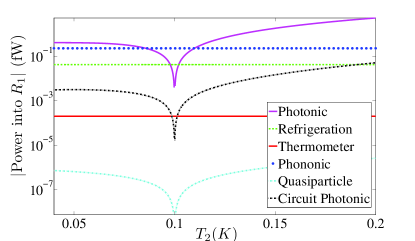
In Fig. 2, the power into Resistor 1 from each of the thermal power sources in Sec. II is compared in the case of and . The temperature of Resistor 2 is scanned from to and the refrigeration bias across a single SIN junction at Resistor 1 is set to . The resistors have a volume of and are placed in a cavity of length , where they are offset at from its ends. For the resistors, we employ the parameters of which we take to have a material parameter of . The cavity has inductance per unit length of and a capacitance per unit length of with the fundamental mode frequency, . The normal-state resistance of the SIN tunnel junctions are , the suppression of the electron–phonon coupling , and the superconducting heat conductivity, as used in Ref. Timofeev et al., 2009. We use a thermometer bias current of and take a smearing parameter . For the aluminium center conductor we take and an energy gap, of . In this setup, the normal-state resistance of the superconducting line with a cross sectional area of is . It is apparent that with these parameters it is the phonon and photon powers that are significant, with the refrigeration and junction lead power being low. We may also conclude that the thermometer power and quasiparticle powers are negligible. However when the magnitude of the bias is greater than , i.e., the Fermi level of the resistor is shifted above the superconductor gap, there is a large increase in and the refrigeration power can be the dominant term. Since Resistor 2 has no refrigeration probe, this only affects Resistor 1.
| Quantity | Value |
|---|---|
| Cavity length, L | |
| Inductance per unit length, | |
| Capacitance per unit length, | |
| Thermometer Bias Current, | |
| Junction lead series capacitance, | |
| Cross-sectional area of line, A | |
| Smearing parameter, | |
| Resitor volume, | |
| Superconductor conductivity, | |
| Superconducting gap of Al, | |
| Al material parameter, | |
| parameter, | |
| Normal state resistance of line, | . |
| Normal state NIS junction resistance, |
III Temperature Response of the resistor
In the steady state, there is no net power flow at Resistors 1 and 2, and hence we have the coupled pair of equations
| (9) | |||
| (10) |
The factors of 2 arise because there are two thermometer and two refrigerator probes.
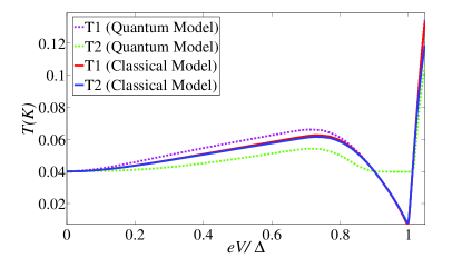
We do not impose a priori the restriction that is fixed, but solve Eqs. (9) and (10) together to find the equilibrium values for and as a function of the refrigerator bias, , on the first resistor. This is precisely what is done in Ref. Timofeev et al., 2009 using a classical photonic powerSchmidt et al. (2004) for the case of two resistors in an impedance matched superconducting loop. The latter setup allows the full quantum of thermal conductance to be achieved, i.e., the maximum possible power transfer via a single one-dimensional photonic channel. In Fig. 3, we observe that the temperatures resulting from the classical photon power used in Ref. Timofeev et al., 2009 give different results to the quantum photonic power given by Eq. (2) at . The heating below the gap is due to the leakage current caused by the smearing of the density of states, and dissapears for .
Let us simulate the single-photon heat conduction experiment proposed in Ref. Jones et al., 2012 including also the refrigeration, thermometer, junction lead and quasiparticle power sources in addition to the phonon and photonic heat power. Since Eq. (10) does not depend on the refrigeration bias, with held fixed, it may be solved for at a given . With this , Eq. (9) can then be solved to find the required SIN refrigeration voltage to make the equations consistent.
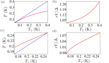
(b) Corresponding heating bias which must be applied to Resistor 1. (c) Single-photon cooling of Resistor 2 is observed when the temperature of Resistor 1 is swept from to for the bath temperature . (d) Corresponding cooling bias which must be applied to Resistor 1. Deviations in due to the effect of the additional thermometer, junction and quasiparticle power sources are indistinguishable in practice. The parameters employed for the cavity are summarized in Table 1.
The results are shown in Fig. 4. The inclusion of the additional power sources has very little effect on the equilibrium value of . Instead the major consequence of incorporating the probes into the model is that it restricts the regime of consistent solutions for photonic cooling of Resistor 2. With a bath temperature of it is possible to find solutions only for . Nevertheless, the temperature range is sufficient for the observation of single-photon cooling, as shown in Fig. 4(c). The bias voltages needed to make the equations consistent are comfortably achievable in practiceTimofeev et al. (2009).
IV Photon Mode Distortion Due To a Capacitor
We first demonstrate that placing electrical components in a cavity changes the spatial profile of the photon modes. This has profound effects, e.g., on the power transfer. We begin by simulating the system in which we partition our transmission line into two coupled cavities. We employ here the model of the transmission line as an infinite series of lumped LC elements. In order to divide this waveguide into two seperate cavities we add a capacitive break of magnitude into the center conductor of the coplanar waveguide as shown in Fig. 5.
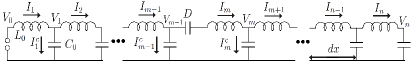
With the capacitor placed at position index , we look for solutions of the form , where and are the angular frequency and phase of the mode respectively. By applying Kirchoff’s laws at each node we obtain the eigensystem
| (11) | |||
| (12) |
Therefore, with no resistors in the cavities, we have an eigenvalue equation for the spatial dependence of the current, , where the matrix is of the form
| (13) |
Here is the matrix without the presence of the capacitor which has the from of a discretized Laplacian and denotes the single-entry matrix with the only non-vanishing element equal to unity at .
We observe that the important factor is the ratio of the intrinsic capacitance to the coupling capacitance . In the limit we return to the matrix for the unmodified cavity, and in the limit , we have two independent cavities.
This system may be solved analytically for any number of capacitors in arbitrary positions. In the case in which one capacitor is placed at we have
where is a normalisation constant and the wavevector is found from
| (14) |
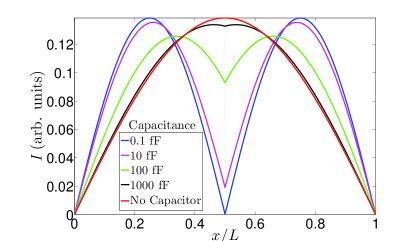
Figure 6 shows the effect on the current profile of the fundamental mode when capacitors of various sizes are placed into a transmission line. The spatial profile is a sensitive function of both capacitor size and position. For small capacitance the current modes are vastly altered. As the capacitance is increased the profile tends back towards that of the unmodified line, as expected.
V Effect of the capacitor on the power transfer
Let us add a resistor of size to the circuit of Fig. 5 at position index . We repeat the procedure of applying Kirchoff’s laws at this node. Due to the finite temperature of the resistor we associate a fluctuating noise voltage across it. We obtain
| (15) |
To study the base effect on the mode profile, we first assume that the resistor does not introduce any noise by setting . In this case, Eq. (15) along with Eqs. (11) and (12) form the system . Here is an impedance matrix given by
| (16) |
For non-trivial we then have the condition that , yielding
the eigenfrequencies of the cavity. This allows to be constructed, from which the current may be found.
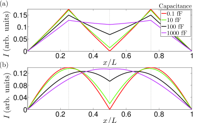
Figure 7(a) shows that adding a resistor of into the center conductor of the transmission line changes the mode profile substantially. The coupling between the resistor and cavity is strong enough for the eigenfrequencies of the modes to have a dominant imaginary component, hence these solutions are found to be rapidly decaying. In Fig. 7(b), we simulate the same system but with . Comparison of the two figures shows that the distortion of the mode is almost negligible in the latter case. This is likely to be the reason for the previously observed discrepancy between the photonic power transfer in the classical and quantum models in the strong-coupling regimeJones et al. (2012). In order to remain in the weak-coupling limit, either the magnitude of the resistor should be small or the resistor should be positioned in the cavity at a point where the amplitude of the mode is small. In Sec. III and Ref. Jones et al., 2012, the constraint that the resistors must remain close to the ends of the cavity ensures this. Otherwise, even in these simple setups it is possible to create vastly different spatial mode profiles simply by altering the position and magnitude of the components.
Next we account for the voltage noise from the resistors. To handle we move into the frequency domain, where the current is governed by the matrix equation . In our case, the fluctuations are due to the Johnson–Nyquist noise, with the power spectrum
| (17) |
with being the temperature of the resistor. If a second resistor is placed into the line, the above procedure can be applied independently to both resistors in order to construct the impedance matrix, and thus the exchanged heat power may be calculated asJones et al. (2012)
| (18) |
The results for the power transfer between two resistors are shown in Fig. 8 for the setup in which a capacitor in the center of the cavity is flanked by the two resistors at and . The introduction of the capacitor reduces the power in comparison to the case of just one cavity. Note that with the resistors at the ends of the cavity, the coupling to the fundamental mode is weaker so that the imaginary part of the eigenfrequency no longer dominates for .
VI Tunable Heat Transport
In this section, we show that the power transfer between two resistors in a cavity may be tuned in situ by placing a SQUID into the line. The transition rates for the absorption and emission of photons between the cavity and the resistors, given in Eq. (3) are functions of the effective impedance of the center conductor. This suggests that by inserting SQUIDs into the line, we can change this effective impedance and therefore vary the coupling strength between the resistors in situ.
Since we have only a few photons in the cavity we are comfortably in the low power regime. Following Ref. Palacios-Laloy et al., 2008, we may then characterise a SQUID with critical current , and loop-inductance , as a linear inductor, provided . In this case the inductance of the SQUID is given by
| (19) |
which depends on the flux through the SQUID via the effective critical current, , with being the flux quantum. In a real SQUID, even with negligible , there is always a slight assymmetry in the critical currents of the junctions and . As a consequence of this assymmetry, is bounded from below by and is therefore never identically zero in practice222The lower bound given by the asymmetry can be circumvented using a so-called balanced SQUID with three Josephson junctionsKemppinen et al. (2008). As is constant for a given we may, assuming small spatial dimensions for the SQUIDs, transform simply by replacing with in the circuit shown in Fig. 5 at any point in the line in which we place a SQUID. This is valid if the capacitance of the SQUID, , is small enough such that .
For simplicity we take the case in which we have only one SQUID in the line, which also distorts the mode profile. This effect is small for most values of but can be substantial at certain resonance points.
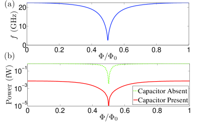
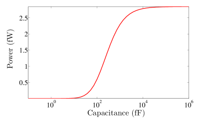
Again we may use Eq. (18) to calculate the photonic power transfer. In Fig. 9(a), the eigenfrequency of the cavity is shown as a function of the flux through the SQUID and Fig. 9(b) shows how the power can be modulated by the flux. We obtain peaks in the power exchange when on resonance. Although the maximum power may seem small, the power dissipated for a single photon in a very high quality factor cavity is of the order . For illustration, a cavity with a quality factor of (see Ref. Megrant et al., 2012), if we again take , has which is less than, or comparable with the powers observed in Fig. 9(b). An example of utilization would be to tune the cavity with the SQUID off resonance whilst we perform an experiment on the other half of the cavity. Afterwards, the SQUID cavity may be tuned back into resonance in order to reset the state of the high-Q cavity without the SQUID. For observation of tunable temperature changes in the resistor, the capacitor is not necessary and its removal increases the power by several orders of magnitude as shown in Fig. 9(b).
VII Conclusions
In summary, we have used a simple circuit model in order to demonstrate that the photonic power between two components in a cavity may be tuned on and off using a SQUID. Furthermore, cavity experiments often involve components which are coupled strongly to the cavity modes. These component can have a substantial impact on the mode profiles such that they no longer bear any relation to the sinusoidal profile of the bare cavity. We have also shown that SIN thermometry does not hinder the ability to observe single-photon heat conduction.
Acknowledgements.
We thank the Academy of Finland, the Emil Aaltonen Foundation, the Finnish National Doctoral Programme in Materials Physics (NGSMP) and the European Research Council under Grant Agreement No. 278117 (SINGLEOUT) for financial support.References
- Blais et al. (2004) A. Blais, R. S. Huang, A. Wallraff, S. M. Girvin, and R. J. Schoelkopf, Phys. Rev. A 69, 62320 (2004).
- Wallraff et al. (2004) A. Wallraff, D. I. Schuster, A. Blais, L. Frunzio, R. S. Huang, J. Majer, S. Kumar, S. M. Girvin, and R. J. Schoelkopf, Nature (London) 431, 162 (2004).
- Blais et al. (2007) A. Blais, J. Gambetta, A. Wallraff, D. I. Schuster, S. M. Girvin, M. H. Devoret, and R. J. Schoelkopf, Phys. Rev. A. 75, 032329 (2007).
- Deppe et al. (2008) F. Deppe, M. Mariantoni, E. P. Menzel, A. Marx, S. Saito, K. Kakuyanagi, H. Tanaka, T. Meno, K. Semba, H. Takayanagi, et al., Nature Phys. 4, 686 (2008).
- Fink et al. (2008) J. M. Fink, M. Goeppl, M. Baur, R. Bianchetti, P. J. Leek, A. Blais, and A. Wallraff, Nature (London) 454, 315 (2008).
- Mariantoni et al. (2011a) M. Mariantoni, H. Wang, R. C. Bialczak, M. Lenander, E. Lucero, M. Neeley, A. D. O’Connell, D. Sank, M. Weides, J. Wenner, et al., Nature Phys. 7, 287 (2011a).
- Paik et al. (2011) H. Paik, D. I. Schuster, L. S. Bishop, G. Kirchmair, G. Catelani, A. P. Sears, B. R. Johnson, M. J. Reagor, L. Frunzio, L. I. Glazman, et al., Phys. Rev. Lett. 107 (2011).
- Niemczyk et al. (2010) T. Niemczyk, F. Deppe, H. Huebl, E. P. Menzel, F. Hocke, M. J. Schwarz, J. J. Garcia-Ripoll, D. Zueco, T. Huemmer, E. Solano, et al., Nature Phys. 6, 772 (2010).
- Meschke et al. (2006) M. Meschke, W. Guichard, and J. P. Pekola, Nature (London) 444, 187 (2006).
- Ojanen and Heikkilä (2007) T. Ojanen and T. T. Heikkilä, Phys. Rev. B 76, 073414 (2007).
- Schmidt et al. (2004) D. R. Schmidt, R. J. Schoelkopf, and A. N. Cleland, Phys. Rev. Lett. 93, 045901 (2004).
- Pascal et al. (2011) L. M. A. Pascal, H. Courtois, and F. W. J. Hekking, Phys. Rev. B 83, 125113 (2011).
- Muhonen et al. (2012) J. T. Muhonen, M. Meschke, and J. P. Pekola, Rep. Prog. Phys. 75, 046501 (2012).
- Jones et al. (2012) P. J. Jones, J. A. M. Huhtamäki, K. Y. Tan, and M. Möttönen, Phys. Rev. B 85, 075413 (2012).
- Houck et al. (2007) A. A. Houck, D. I. Schuster, J. M. Gambetta, J. A. Schreier, B. R. Johnson, J. M. Chow, L. Frunzio, J. Majer, M. H. Devoret, S. M. Girvin, et al., Nature (London) 449, 328 (2007).
- Hofheinz et al. (2008) M. Hofheinz, E. M. Weig, M. Ansmann, R. C. Bialczak, E. Lucero, M. Neeley, A. D. O’Connell, H. Wang, J. M. Martinis, and A. N. Cleland, Nature (London) 454, 310 (2008).
- Hofheinz et al. (2009) M. Hofheinz, H. Wang, M. Ansmann, R. C. Bialczak, E. Lucero, M. Neeley, A. D. O’Connell, D. Sank, J. Wenner, J. M. Martinis, et al., Nature (London) 459, 546 (2009).
- Schuster et al. (2007) D. I. Schuster, A. A. Houck, J. A. Schreier, A. Wallraff, J. M. Gambetta, A. Blais, L. Frunzio, J. Majer, B. Johnson, M. H. Devoret, et al., Nature (London) 445, 515 (2007).
- Bozyigit et al. (2011) D. Bozyigit, C. Lang, L. Steffen, J. M. Fink, C. Eichler, M. Baur, R. Bianchetti, P. J. Leek, S. Filipp, M. P. da Silva, et al., Nature Phys. 7, 154 (2011).
- Chen et al. (2011) Y. F. Chen, D. Hover, S. Sendelbach, L. Maurer, S. T. Merkel, E. J. Pritchett, F. K. Wilhelm, and R. McDermott, Phys. Rev. Lett. 107 (2011).
- Giazotto et al. (2006) F. Giazotto, T. T. Heikkilä, A. Luukanen, A. M. Savin, and J. P. Pekola, Rev. Mod. Phys. 78, 217 (2006).
- Mariantoni et al. (2011b) M. Mariantoni, H. Wang, T. Yamamoto, M. Neeley, R. C. Bialczak, Y. Chen, M. Lenander, E. Lucero, A. D. O’Connell, D. Sank, et al., Science 334, 61 (2011b).
- Yang et al. (2003) C. P. Yang, S. I. Chu, and S. Y. Han, Phys. Rev. A 67, 042311 (2003).
- Zhou et al. (2002) Z. Y. Zhou, S. I. Chu, and S. Y. Han, Phys Rev B 66, 054527 (2002).
- Chiorescu et al. (2004) I. Chiorescu, P. Bertet, K. Semba, Y. Nakamura, C. J. P. M. Harmans, and J. E. Mooij, Nature (London) 431, 159 (2004).
- Castellanos-Beltrana and Lehnert (2007) M. A. Castellanos-Beltrana and K. W. Lehnert, App. Phys. Lett. 91 (2007).
- Sandberg et al. (2008) M. Sandberg, C. M. Wilson, F. Persson, T. Bauch, G. Johansson, V. Shumeiko, T. Duty, and P. Delsing, App. Phys. Lett. 92 (2008).
- Wilson et al. (2011) C. M. Wilson, G. Johansson, A. Pourkabirian, M. Simoen, J. R. Johansson, T. Duty, F. Nori, and P. Delsing, Nature (London) 479, 376 (2011).
- Zakka-Bajjani et al. (2011) E. Zakka-Bajjani, F. Nguyen, M. Lee, L. R. Vale, R. Simmonds, and J. Aumentado, Nature Phys. 7, 599 (2011).
- Palacios-Laloy et al. (2008) A. Palacios-Laloy, F. Nguyen, F. Mallet, P. Bertet, D. Vion, and D. Esteve, J. Low Temp. Phys. 151, 1034 (2008).
- Leivo et al. (1996) M. M. Leivo, J. P. Pekola, and D. V. Averin, App. Phys. Lett. 68, 1996 (1996).
- Dynes et al. (1984) R. Dynes, J. Garno, G. Hertel, and T. Orlando, Phys. Rev. Lett. 53, 2437 (1984).
- Pekola et al. (2010) J. P. Pekola, V. F. Maisi, S. Kafanov, N. Chekurov, A. Kemppinen, Y. A. Pashkin, O.-P. Saira, M. Möttönen, and J. S. Tsai, Phys. Rev. Lett. 105, 026803 (2010).
- Pekola (2004) J. Pekola, J. Low Temp. Phys. 135, 723 (2004).
- Not (a) This circuit model is a rather crude approximation, nevertheless, it should give a reasonable order of magnitude estimate. In any case, such a model should only overestimate this photonic power contribution.
- Timofeev et al. (2009) A. V. Timofeev, M. Helle, M. Meschke, M. Möttönen, and J. P. Pekola, Phys. Rev. Lett. 102, 200801 (2009).
- Saira et al. (2012) O.-P. Saira, A. Kemppinen, V. F. Maisi, and J. P. Pekola, Phys. Rev. B 85, 012504 (2012).
- Not (b) The lower bound given by the asymmetry can be circumvented using a so-called balanced SQUID with three Josephson junctionsKemppinen et al. (2008).
- Megrant et al. (2012) A. Megrant, C. Neill, R. Barends, B. Chiaro, Y. Chen, L. Feigl, J. Kelly, E. Lucero, M. Mariantoni, P. J. J. O’Malley, et al., App. Phys. Lett. 100, 113510 (2012).
- Kemppinen et al. (2008) A. Kemppinen, A. J. Manninen, M. Möttönen, J. J. Vartiainen, J. T. Peltonen, and J. P. Pekola, App. Phys. Lett. 92 (2008).