Intrinsic Ultrathin Topological Insulators Grown via MBE Characterized by in-situ Angle Resolved Photoemission Spectroscopy
Abstract
We demonstrate the capability of growing high quality ultrathin (QL 10) films of the topological insulators Bi2Se3 and Bi2Te3 using molecular beam epitaxy. Unlike previous growth techniques, which often pin the Fermi energy in the conduction band for ultrathin samples, our samples remain intrinsic bulk insulators. We characterize these films using in-situ angle resolved photoemission spectroscopy (ARPES), which is a direct probe of bandstructure, and ex-situ atomic force microscopy. We find that the conduction band lies above the Fermi energy, indicating bulk insulating behavior with only the surface states crossing EF. We conclude that thermal cracking of Te and Se in our growth leads to higher quality thin films, paving the way for future improvements in growth of topological insulators.
Topological insulators are a recently discovered class of materials exhibiting unique surface states which are strongly protected against perturbations in either the material bulk or on the surface Hasan and Kane (2010); Qi and Zhang (2011); Fu et al. (2007); Xia et al. (2009); Chen et al. (2009); Zhang et al. (2009a); Wray et al. (2011); Hsieh et al. (2009a). These states are characterized by a linear electronic dispersion where the electron’s spin is locked to its momentum direction. The surface states expand across the bulk band gap and intersect to form a Dirac cone centered around . Ideally, the Fermi level will cross the surface states inside the bulk band gap, making the material a surface metal. Experimentally, however, such materials often have the Fermi energy pinned into the bulk conduction band or have a conduction surface state coexist with the topological surface stateChen et al. (2009); Xia et al. (2009); Bianchi et al. (2010). For the parent compounds Bi2Se3 and Bi2Te3, such pinning of the Fermi energy has been attributed to bulk crystal defectsHor et al. (2009). Thus, an important experimental challenge has been to reduce the contribution of bulk carriers such that the surface states dominate transport properties.
Because Bi2Se3 and Bi2Te3 possess a layered rhombohedral structure, a large effort has been focused on thin film growth techniques such as molecular beam epitaxy to reduce crystal defectsZhang et al. (2009b); Wang et al. (2011); Krumrain et al. (2011); Bansal et al. (2011). Most thin film growth previously reported have made use of thermal effusion cells. However, when selenium or tellurium are evaporated in vacuum, they form molecular complexes of variable atomic number, most commonly Te2/Se2 Li et al. (2010); Krumrain et al. (2011); Bansal et al. (2011). This often requires a larger Se2/Te2 flux be added to compensate, often in a ratio greater than 10 Te2/Se2 to 1 BiBansal et al. (2011); Krumrain et al. (2011). In addition, such growth methods still tend to pin the Fermi energy to some level above the conduction band, thus reducing the contribution of the topological surface state to transportLi et al. (2010); Zhang et al. (2010). Traditionally, dopants have been added to the crystal growth to tune the Fermi energy of the system into the bulk gapArakane et al. (2012); Ren et al. (2011); Zhang et al. (2011); Hsieh et al. (2009b). This letter reports on recent advances in growth of intrinsic topological insulator parent compounds Bi2Se3 and Bi2Te3 using a selenium and tellurium thermal cracker effusion cell, which to the authors’ knowledge, has not been explicitly reported in previous works. Combined with high energy resolution, in-situ angle-resolved photoemission spectroscopy, we demonstrate that films grown this way have their Fermi energy located within the bulk gap.
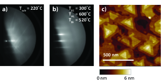
Figure 1 shows the growth conditions of Bi2Te3. The substrate used was a sapphire-0001 substrate cleaned for 1.5 hours at 650∘, followed by 30 minutes at 900∘ C. The effusion cell used during growth contains a hot lip with a cracking insert which helps break Te2/Se2 molecular flux into atomic Te/Se. We grow with flux ratios that are much more stoichiometric than previous groups (2 Te/Se to 1 Bi). We find that growth rate is controlled via the bismuth flux, as reported in ref Krumrain et al. (2011); Li et al. (2010). However, exceedingly large Te fluxes produced lower quality growth, manifested by broader and weaker surface dispersion spectra. Figure 1(a) shows reflection high-energy electron diffraction pattern of the bare sapphire substrate. Figure 1(b) shows the RHEED pattern after several minutes of growth. The streak intensities show clear oscillations (not shown), indicative of epitaxial growth, with an oscillation period of approximately 50 seconds. Bi2Te3 films grown for this study ranged from 5 to 10 QL, with similar electronic structure. Figure 1(c) shows the AFM image of a 10 QL sample taken ex-situ. Clear trianglular islands can be resolved in the topmost two layers, while the lower layers have nearly full coverage.
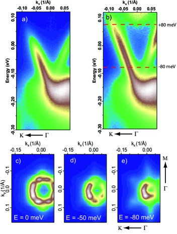
Electronic properties of such thin films are often studied ex-situ through transport or quantum oscillationsLiu et al. (2011). However, to determine the Fermi level and obtain bandstructure directly, we use angle resolved photoemission spectroscopy (ARPES) Damascelli et al. (2003). Due to ARPES’s extreme surface sensitivity, such measurements are ideally performed in situ. Previous in-situ ARPES measurements on ultrathin films, whose thicknesses are less than 20-30 quintuple layers, have revealed a bulk conduction band or quantum well statesLi et al. (2010); Zhang et al. (2010); Plucinski et al. (2011); Chang et al. (2011). These quantum well states are due to confinement along the c-axis in films of thicknesses around 5 QL. In our setup, a Scienta R2002 electron analyzer was used with a 7 eV laser light source. Fermi energies were determined using a gold spectra, with 5 meV resolution. Figure 2(a) shows the electron dispersion along a high symmetry axis from to K, taken 4 hours after growth, at room temperature. The Dirac cone can be clearly distinguished, intersecting with the valence band. Noticeably there is no signature of the conduction band. To determine the location of the conduction band, we use thermal population of states above the Fermi energy. Figure 2(b) plots the spectra of 2(a) after factoring out the Fermi-Dirac function at room temperature. We can thus resolve the bulk conduction band to be approximately 80 meV above the Fermi energy. Furthermore we can determine the location of the valence band through mapping the entire 2D bandstructure and examining the appearance of the valence band away from the gamma point. Figures 2(c)-(e) are such mappings at different binding energies. 2(c), at 0 meV, shows the Fermi surface, which reveals no trace of the bulk conduction band state often seen in other materials grown by other methods. In 2(d), which is 50 meV below the Fermi energy, one can see the formation of the Dirac cone. Finally, in figure 2(e), at 80 meV below the fermi energy, one sees the appearance of the hexagonal bulk valence band stateChen et al. (2009). Our data thus gives a bulk gap of approximately 160 meV, from valence band maximum to conduction band minimum. Such a gap is consistent with previous experimental results at other photon energiesChen et al. (2009); Li et al. (2010). We therefore conclude our Fermi energy lies exactly midgap.
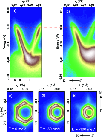
It has been previously reported that Bi2Te3 exhibits a downward band-bending as one decreases temperatureLi et al. (2010); Park et al. (2011). To measure the temperature dependence we map the bandstructure at 150K. Data were taken approximately 24 hours after growth. Figure 3(a) plots the dispersion from to K. 3(b) is a reproduction of 2(b) for comparison. Figures 3(c)-(e) show constant energy mappings. The fermi surface has attained a noticeable hexagonal shape, consistent with previous low temperature measurements Chen et al. (2012, 2009). Scanning through constant-energy maps with increasing binding energy, we see the appearance of the valence band at approximately 100 meV below the surface, shown in figure 3(e). This indicates a band shift of approximately 20 meV from 300K to 150K. Due to measuring at lower temperature, we cannot use thermal population to observe the conduction band. The momentum distribution curve linewidths do not broaden, indicating little to no aging, which has otherwise been previously reported in such bulk systems Chen et al. (2012); Hsieh et al. (2009a). Overall, the effects of aging in vacuum and temperature variation do not affect the Fermi level to the point where our film is degenerately doped. In addition, we find that variations in substrate temperatures on the order of 40 degrees do not send the Fermi level outside the gap.
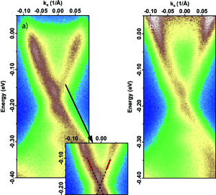
In addition to growing ultrathin films of Bi2Te3, we also grow Bi2Se3 using a thermal cracker cell. Following similar procedures and flux ratios, and using the same substrate, we grow films with thicknesses ranging from 6-8 QL. ARPES spectra of an 8 QL film are plotted in figure 4. Figure 4(a) shows the dispersion along the -K axis at 250K. To determine the Dirac point, we fit the momentum distribution peaks of the surface states to a linear dispersion near the dirac point (inset of figure 4(a)). The intersection of the linear dispersions determines the Dirac point. We find the Dirac point lies approximately 190 meV below the Fermi energy. Previous work on bulk samples has shown the conduction band to lie 200-220 meV above the Dirac point Xia et al. (2009); Bianchi et al. (2010); Park et al. (2011, 2010), again above our Fermi energy. Figure 4(b) shows the spectrum after factoring out the Fermi-Dirac function. Using this normalized spectrum we find at energies 10-20 meV above EF an increase in linewidth of the surface states bands. This is indicative of surface state to bulk state scattering Park et al. (2011), and hence gives a signature of the bulk band bottom. Hence surface conduction from non-topological surface states is dramatically reduced. Given a temperature low enough to avoid thermal population, one would expect bulk conduction to be small. Other films grown in this study exhibited similar electronic structure.
In summary, we have demonstrated the ability to grow high quality ultra-thin films of the topological insulators Bi2Se3 and Bi2Te3 using a thermal cracker effusion cell. With in-situ high resolution ARPES, we characterized the quality of the films immediately after growth by mapping the band structure. For our undoped, as grown films of Bi2Te3, the Fermi energy was always located well-within the bulk gap. Lowering of temperature causes a rigid shift of the bands towards n-type by approximately 20 meV, but leaves the overall band structure, doping and TI properties intact. For Bi2Se3, growth of films show the conduction band to be 10-20 meV above EF. The use of thermal cracker cells to grow our materials should pave the way for better materials growth of topological insulators, and opens up a wide range of possibilities not only scientifically but also from an applied perspective, since ultrathin films of sufficient quality and stability for surface-dominated transport can be fabricated for further study.
This work is supported by DOE office of Basic Energy Science, Division of Materials Science.
References
- Hasan and Kane (2010) M. Z. Hasan and C. L. Kane, Rev. Mod. Phys. 82, 3045 (2010).
- Qi and Zhang (2011) X.-L. Qi and S.-C. Zhang, Rev. Mod. Phys. 83, 1057 (2011).
- Fu et al. (2007) L. Fu, C. L. Kane, and E. J. Mele, Phys. Rev. Lett. 98, 106803 (2007).
- Xia et al. (2009) Y. Xia, D. Qian, D. Hsieh, L. Wray, A. Pal, H. Lin, A. Bansil, D. Grauer, Y. S. Hor, R. J. Cava, and M. Z. Hasan, NATURE PHYSICS 5, 398 (2009).
- Chen et al. (2009) Y. L. Chen, J. G. Analytis, J.-H. Chu, Z. K. Liu, S.-K. Mo, X. L. Qi, H. J. Zhang, D. H. Lu, X. Dai, Z. Fang, S. C. Zhang, I. R. Fisher, Z. Hussain, and Z.-X. Shen, Science 325, 178 (2009), http://www.sciencemag.org/content/325/5937/178.full.pdf .
- Zhang et al. (2009a) H. Zhang, C.-X. Liu, X.-L. Qi, X. Dai, Z. Fang, and S.-C. Zhang, NATURE PHYSICS 5, 438 (2009a).
- Wray et al. (2011) L. A. Wray, S.-Y. Xu, Y. Xia, D. Hsieh, A. V. Fedorov, Y. S. Hor, R. J. Cava, A. Bansil, H. Lin, and M. Z. Hasan, NATURE PHYSICS 7, 32 (2011).
- Hsieh et al. (2009a) D. Hsieh, Y. Xia, D. Qian, L. Wray, F. Meier, J. H. Dil, J. Osterwalder, L. Patthey, A. V. Fedorov, H. Lin, A. Bansil, D. Grauer, Y. S. Hor, R. J. Cava, and M. Z. Hasan, Phys. Rev. Lett. 103, 146401 (2009a).
- Bianchi et al. (2010) M. Bianchi, D. Guan, S. Bao, J. Mi, B. B. Iversen, P. D. C. King, and P. Hofmann, NATURE COMMUNICATIONS 1 (2010), 10.1038/ncomms1131.
- Hor et al. (2009) Y. S. Hor, A. Richardella, P. Roushan, Y. Xia, J. G. Checkelsky, A. Yazdani, M. Z. Hasan, N. P. Ong, and R. J. Cava, Phys. Rev. B 79, 195208 (2009).
- Zhang et al. (2009b) G. Zhang, H. Qin, J. Teng, J. Guo, Q. Guo, X. Dai, Z. Fang, and K. Wu, Applied Physics Letters 95, 053114 (2009b).
- Wang et al. (2011) G. Wang, X.-G. Zhu, Y.-Y. Sun, Y.-Y. Li, T. Zhang, J. Wen, X. Chen, K. He, L.-L. Wang, X.-C. Ma, J.-F. Jia, S. B. Zhang, and Q.-K. Xue, Advanced Materials 23, 2929 (2011).
- Krumrain et al. (2011) J. Krumrain, G. Mussler, S. Borisova, T. Stoica, L. Plucinski, C. Schneider, and D. Gr tzmacher, Journal of Crystal Growth 324, 115 (2011).
- Bansal et al. (2011) N. Bansal, Y. S. Kim, E. Edrey, M. Brahlek, Y. Horibe, K. Iida, M. Tanimura, G.-H. Li, T. Feng, H.-D. Lee, T. Gustafsson, E. Andrei, and S. Oh, Thin Solid Films 520, 224 (2011).
- Li et al. (2010) Y.-Y. Li, G. Wang, X.-G. Zhu, M.-H. Liu, C. Ye, X. Chen, Y.-Y. Wang, K. He, L.-L. Wang, X.-C. Ma, H.-J. Zhang, X. Dai, Z. Fang, X.-C. Xie, Y. Liu, X.-L. Qi, J.-F. Jia, S.-C. Zhang, and Q.-K. Xue, Advanced Materials 22, 4002 (2010).
- Zhang et al. (2010) Y. Zhang, K. He, C.-Z. Chang, C.-L. Song, L.-L. Wang, X. Chen, J.-F. Jia, Z. Fang, X. Dai, W.-Y. Shan, S.-Q. Shen, Q. Niu, X.-L. Qi, S.-C. Zhang, X.-C. Ma, and Q.-K. Xue, NATURE PHYSICS 6 (2010).
- Arakane et al. (2012) T. Arakane, T. Sato, S. Souma, K. Kosaka, K. Nakayama, M. Komatsu, T. Takahashi, Z. Ren, K. Segawa, and Y. Ando, NATURE COMMUNICATIONS 3 (2012), 10.1038/ncomms1639.
- Ren et al. (2011) Z. Ren, A. A. Taskin, S. Sasaki, K. Segawa, and Y. Ando, Phys. Rev. B 84, 165311 (2011).
- Zhang et al. (2011) J. Zhang, C.-Z. Chang, Z. Zhang, J. Wen, X. Feng, K. Li, M. Liu, K. He, L. Wang, X. Chen, Q.-K. Xue, X. Ma, and Y. Wang, NATURE COMMUNICATIONS 2 (2011), 10.1038/ncomms1588.
- Hsieh et al. (2009b) D. Hsieh, Y. Xia, D. Qian, L. Wray, J. H. Dil, F. Meier, J. Osterwalder, L. Patthey, J. G. Checkelsky, N. P. Ong, A. V. Fedorov, H. Lin, A. Bansil, D. Grauer, Y. S. Hor, R. J. Cava, and M. Z. Hasan, NATURE 460, 1101 (2009b).
- Liu et al. (2011) M. Liu, C.-Z. Chang, Z. Zhang, Y. Zhang, W. Ruan, K. He, L.-l. Wang, X. Chen, J.-F. Jia, S.-C. Zhang, Q.-K. Xue, X. Ma, and Y. Wang, Phys. Rev. B 83, 165440 (2011).
- Damascelli et al. (2003) A. Damascelli, Z. Hussain, and Z.-X. Shen, Rev. Mod. Phys. 75, 473 (2003).
- Plucinski et al. (2011) L. Plucinski, G. Mussler, J. Krumrain, A. Herdt, S. Suga, D. Grutzmacher, and C. M. Schneider, Applied Physics Letters 98, 222503 (2011).
- Chang et al. (2011) C. Chang, K. He, L. L. Wang, and X. Ma, SPIN 1, 21 (2011).
- Park et al. (2011) S. R. Park, W. S. Jung, G. R. Han, Y. K. Kim, C. Kim, D. J. Song, Y. Y. Koh, S. Kimura, K. D. Lee, N. Hur, J. Y. Kim, B. K. Cho, J. H. Kim, Y. S. Kwon, J. H. Han, and C. Kim, New Journal of Physics 13, 013008 (2011).
- Chen et al. (2012) C. Chen, S. He, H. Weng, W. Zhang, L. Zhao, H. Liu, X. Jia, D. Mou, S. Liu, J. He, Y. Peng, Y. Feng, Z. Xie, G. Liu, X. Dong, J. Zhang, X. Wang, Q. Peng, Z. Wang, S. Zhang, F. Yang, C. Chen, Z. Xu, X. Dai, Z. Fang, and X. J. Zhou, Proceedings of the National Academy of Sciences 109, 3694 (2012), http://www.pnas.org/content/109/10/3694.full.pdf+html .
- Park et al. (2010) S. R. Park, W. S. Jung, C. Kim, D. J. Song, C. Kim, S. Kimura, K. D. Lee, and N. Hur, Phys. Rev. B 81, 041405 (2010).