Electronic structure of CrN: A comparison between different exchange correlation potentials
Abstract
We report a series of electronic structure calculations for CrN using different exchange correlation potentials: PBE, LDA+, the Tran-Blaha modified Becke-Johnson, and hybrid functionals. In every case, our calculations show that the onset of magnetism in CrN should be accompanied by a gap opening. The experimentally found antiferromagnetic order always leads to an insulating behavior. Our results give further evidence that the Tran-Blaha functional is very useful for treating the electronic structure of correlated semiconductors allowing a parameter free description of the system. Hybrid functionals are also well capable of describing the electronic structure of CrN. The analysis of the system is complemented with our calculations of the thermopower that are in agreement with the experimental data.
pacs:
71.15.-m, 71.20.-b, 71.27.+aI Introduction
Transition-metal nitrides (TMN) have drawn considerable attention due to their interesting physical properties: mechanical strength, ultrahardness, corrosion resistance, high melting points, good electrical and thermal conductivities, etc.Niewa and DiSalvo (1998) In addition, some TMN exhibit other properties such as superconductivity (arising in VN (Ref. Zhao et al., 1984) and NbN (Ref. Chockalingam et al., 2009; Lascialfari et al., 2009)), a transition from a superconductor to a Cooper pair insulator in TiN (Ref. Baturina et al., 2007), or a magnetostructural phase transition (MPT) as a function of temperature in CrN (Ref. Corliss et al., 1960).
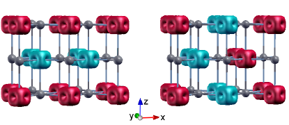
This MPT in CrN has attracted considerable attention and controversial results have been reported. Some studies have shown that this transition is linked to a discontinuity in the resistivity versus temperature curve. Constantin et al. (2004); Quintela et al. (2009, 2010); Bhobe et al. (2010) It has been characterized as a first-order MPT from a high-temperature paramagnetic (PM), cubic NaCl-type phase to a low-temperature antiferromagnetic (AFM) orthorhombic Pnma one at a Néel temperature 273-286 K.Corliss et al. (1960) The low- AFM configuration is quite unique consisting of double ferromagnetic (FM) layers stacked antiferromagnetically along the [110] direction (see AFM2 in the right panel of Fig. 1). From neutron powder diffraction experiments, a magnetic moment of 2.36 per Cr atom was obtained by Corliss et al.,Corliss et al. (1960) while in Ref. Ibberson and Cywinski, 1992 a value of 3.17 was measured. This peculiar magnetic structure has been shown to be linked to the structural distortion across .Filippetti et al. (1999); Filippetti and Hill (2000) However, other works show the suppression of the phase transition due to epitaxial constraints when grown in films with the system remaining in the cubic phase at all temperatures. Gall et al. (2002a); Inumaru et al. (2007); Zhang et al. (2011a)
The main focus of controversy has been the understanding of CrN electrical behavior. On the one hand, the values of the resistivity at room temperature vary over several orders of magnitude (from mcm to kcm) in different works. Anderson et al. (2005); Bhobe et al. (2010); Constantin et al. (2004); Gall et al. (2002a, b); Zhang et al. (2011b, a); Quintela et al. (2009); Tsuchiya et al. (1996); Quintela et al. (2010) On the other, the nature of the transition in terms of the electrical conduction behavior has had a wide range of interpretations in the literature:
Metal to metal. In the work of Tsuchiya et al.,Tsuchiya et al. (1996) polycrystalline CrN1+x films with 0 x 0.2 have been grown by reactive sputtering. Nearly stoichiometric films show an AFM first order phase transition at K. Resistivity measurements for these samples indicated metallic behavior across with a steep decrease of the resistivity below the transition. The same behavior was found by Browne et al. Browne et al. (1970) in CrN powder. In the study of Inumaru et al.,Inumaru et al. (2007) CrN films were epitaxially grown on -Al2O3 (0001) and MgO (001) substrates by pulsed laser deposition. The films grown on -Al2O3 (0001) with its (111) planes parallel to the substrate show no structural transition whereas CrN(001) films grown on MgO (001) show a transition to an AFM state at about 260 K. Both films exhibit metallic -dependence of the resistivity, but a drop in its values below the Néel temperature is observed for the samples showing a MPT.
Metal to semiconductor. Constantin et al.Constantin et al. (2004) grew CrN(001) thin films on MgO(001) using molecular beam epitaxy. The films show a MPT at 285 K, with activated semiconducting behavior above and a band gap of 0.07 eV. Below the transition temperature, the films are metallic. The polycrystalline samples of CrN prepared by Bhobe et al.Bhobe et al. (2010) show a MPT at 286 K. Above , CrN exhibits activated semiconducting behavior (with a gap of 0.07 eV) becoming a disordered metal below . Evidences of strong electron-electron correlations were found, determining an on-site Coulomb energy () of 4.5 eV by resonant photoemission spectroscopy (PES). In Ref. Zhang et al., 2011a both single and polycrystalline CrN layers have been grown by reactive sputtering deposition on both MgO and quartz substrates. Polycrystalline CrN did show a disorder induced metal-insulator transition to an orthorhombic phase across K.
Semiconductor to semiconductor. In the above mentioned work of Tsuchiya et al.,Tsuchiya et al. (1996) the non-stoichiometric films did not show a MPT. The resistivity decreases monotonically with suggesting a semiconducting (hopping-like) behavior of the samples. CrN powder samples synthesized by Herle et al.Herle et al. (1997) show a transition from a PM to an AFM phase at 280 K. Activated semiconducting behavior with a band gap of 0.09 eV was obtained from resistivity vs. curves. Quintela et al.Quintela et al. (2010) studied polycrystalline samples of Cr1-xVxN. Stoichiometric CrN shows a MPT at K and semiconducting behavior in the whole -range. Above , the resistivity vs. curve shows activated semiconducting behavior with a band gap of 150 meV. Below the transition, the changes in the chemical bond linked to the AFM order, give as a result a non-activated semiconducting behavior. The thermoelectric power of stoichiometric CrN shows a linear -dependence as expected for metals or highly degenerate semiconductors. This supports the idea of an electronic state neither thermally activated nor fully itinerant in the AFM phase. Further evidence of this idea is given by the drastic reduction of the bulk modulus due to the bond softening and charge delocalization into the shorter and less strong Cr-Cr bonds in the AFM phase.Rivadulla et al. (2009) By ultrahigh vacuum magnetron sputtering, Gall et al. Gall et al. (2002b, a); Zhang et al. (2011b); Zhang and Gall (2010); Zhang et al. (2011a) grew single crystalline CrN (001) films on a MgO(001) substrate. The absence of any discontinuity in the resistivity vs. curves suggests that epitaxial constraints suppress the transition to an AFM phase with the film being cubic PM at all T. The resistivity decreases with increasing temperature indicating semiconducting behavior over the whole T-range. From optical absorption measurements, an optical band gap of 0.7 eV was obtained.Gall et al. (2002a); Anderson et al. (2005) An indirect band gap of about 0.19 eV was also estimated Zhang and Gall (2010) from optical measurements suggesting CrN is a Mott-Hubbard type insulator. In addition, the samples show semiconducting behavior in a variable range hopping regime below 120 K.Zhang et al. (2011b, a)
As can be seen, there is a big discussion and disagreement between different experimental works. There are also some theoretical studies on CrN. Calculations within the local density approximation (LDA) have been performed on CrN by Filippetti et al.Filippetti et al. (1999); Filippetti and Hill (2000) For the distorted othorhombic structure, they found as ground state the experimentally observed AFM2 configuration. For the cubic structure, the ground state is the so-called AFM1, similar to the AFM2, but with the spins antialigned every layer instead of every two layers (left panel of Fig. 1). This can be understood in terms of the magnetic stress: the AFM2 phase is under more stress with respect to the AFM1. This is due to the spin ordering asymmetry of the AFM2 phase on the (001) plane where each Cr has two spin-antiparallel and two spin-parallel nearest neighbors. Considering that bonds between the antiferromagnetically coupled neighbors are under tensile stress, while bonds between ferromagnetically coupled atoms are under compressive stress, in the AFM2 magnetic configuration, stress can be relieved by an orthorhombic distortion. In the AFM1 structure, it cannot be relieved because all the four-nearest neighbors are FM coupled. Hence, in order to relieve stress and reduce the total energy, the system undergoes a shear distortion from cubic to orthorhombic. LDA calculations show a metallic behavior for both AFM phases (weak metal since the density of states (DOS) at the Fermi level is small). From studies of TM oxides and other correlated compounds it is known that LDA underestimates the Coulomb effects on the narrow bands, predicting an unrealistic metallic state in systems that actually have a band gap. Hence, further electronic structure calculations in CrN within the LDA+Liechtenstein et al. (1995) method were performed by Herwadkar et al.Herwadkar and Lambrecht (2009) If the on-site Coulomb repulsion () is considered, a band gap already opens for a value of eV in the magnetic ground state, suggesting that CrN may be close to a charge-transfer insulator.
To shed light on the existing controversies about CrN, we present the results of renewed ab initio calculations using different computational schemes to treat the moderately correlated electrons of CrN and describe properly its electronic structure and transport properties.
II COMPUTATIONAL DETAILS
Our electronic structure calculations were performed with the WIEN2k code,Blaha et al. (2001); Schwarz and Blaha (2003) based on density functional theory (DFT)Hohenberg and Kohn (1964); Kohn and Sham (1965); Jones and Gunnarsson (1989) utilizing the augmented plane wave plus local orbitals method (APW+lo).Sjöstedt et al. (2000) For the calculations of the transport properties we used the BoltzTraP code,Madsen and Singh (2006) a semiclassical approach based on the Boltzmann transport theory.
Most of the DFT-based calculations in solids have been done using two (semi)local approaches for the exchange correlation energy and potential: local density approximation (LDA)Kohn and Sham (1965) or generalized gradient approximation (GGA).Perdew et al. (1996) Although they give useful total energies and structural parameters, both of them are known to underestimate the band gap of most semiconductors and insulators.
There are several functionals that can provide more accurate values for band gaps. On the one hand, staying inside the true Kohn-Sham (KS) framework (multiplicative potential), the newly developed semilocal potentials (such as the one developed by Tran and Blaha based on a modification of the Becke-JohnsonBecke and Johnson (2006) potential) can give good results.Tran and Blaha (2009); Singh (2010) But on the other hand, nonmultiplicative potentials can also be used. These methods belong to the so-called generalized KS frameworkSeidl et al. (1996) and most of them mix DFT and Hartree-Fock (HF) theories. The most used ones are the LDA+ Liechtenstein et al. (1995) approach and hybrid methods.Becke (1993)
The LDA+ scheme improves over GGA or LDA in the study of systems containing correlated electrons by introducing the on-site Coulomb repulsion applied to localized electrons (e.g or ). We have performed calculations on CrN within the LDA+ method (using the fully localized version for the double-counting correctionCzyżyk and Sawatzky (1994)), taking in a reasonable range for this type of electron systems (from 2 to 5 eV) comparable to the values obtained by PES experiments. The exchange parameter was set to zero.
In hybrid methods a certain amount of semilocal exchange is replaced by HF exchange with the correlation remaining purely semilocal. They usually lead to improved band structures in good agreement with experiments as shown for several semiconductors and insulators or even strongly correlated electron systems.Muscat et al. (2001); de P. R. Moreira et al. (2002); Kudin et al. (2002) We have applied one of the most common hybrid functionals (PBE0)Ernzerhof and Scuseria (1999); Adamo and Barone (1999) to the study of the electronic structure of CrN. However, traditional hybrid functionals are computationally very demanding due to the long-range nature of the HF exchange in solids. A way to reduce this problem of convergence is to consider only the short-range part of the HF exchange as proposed by Bylander and Kleinman.Bylander and Kleinman (1990) This scheme has been used by Heyd, Scuseria, and ErnzerhofHeyd et al. (2003); Heyd and Scuseria (2004) who proposed a screened hybrid functional based on PBE0. We have also performed calculations using a screened hybrid functional as implemented in the WIEN2k code with the HF exchange screened by means of the Yukawa potential (so called, YS-PBE0).Tran and Blaha (2011)
The modified Becke-Johnson exchange potential (a local approximation to an atomic exact-exchange potential and a screening term) + LDA-correlation (from hereon TB-mBJLDA) allows the calculation of band gaps with an accuracy similar to the much more expensive or hybrid methods.Tran and Blaha (2009); Koller et al. (2011); Singh (2010) We have also studied the electronic structure of CrN by using the TB-mBJLDA potential which does not contain any system-dependent parameter.
The calculations were done with (the product of the smallest of the atomic sphere radii and the plane wave cutoff parameter ), which determines the size of the basis set. The chosen were 2.06 an 1.82 for Cr and N, respectively. The PBE, LDA+, and TB-mBJLDA calculations were done with a k-mesh for the integrations over the Brillouin zone. Since calculations with hybrid functionals are much more costly, a less dense k-mesh of was used for the YS-PBE0 and PBE0 functionals. Convergence for the total energies presented is achieved with that k-mesh. The transport properties are very sensitive to the Brillouin zone sampling, therefore an even denser grid () was used to obtain convergence.
As mentioned in Sec. I, the transition at in CrN from the PM to the AFM phase is accompanied by a distortion of the rocksalt structure. The shear distortion consists of a contraction of the angle from the cubic (90∘) to 88.23∘ (see Ref. Filippetti et al., 1999 for a more detailed description). Calculations were done both, with and without distortion at the experimental lattice constants (Ref. Corliss et al., 1960). In order to accomodate the AFM2 phase, a unit cell comprising four formula units has been used. The calculations for the other magnetic phases were also performed with this unit cell.
III RESULTS
| orthorhombic | cubic | |||||||
| AFM2 | AFM1 | FM | NM | AFM2 | AFM1 | FM | NM | |
| Relative energy | ||||||||
| PBE | 0 | 20 | 211 | 504 | 17 | 13 | 208 | 507 |
| LDA+ ( eV) | 0 | 42 | 215 | 1068 | 14 | 35 | 209 | 1074 |
| LDA+ ( eV) | 0 | 49 | 202 | 1540 | 11 | 41 | 194 | 1548 |
| LDA+ ( eV) | 0 | 50 | 180 | 2028 | 8 | 41 | 170 | 2049 |
| LDA+ ( eV) | 0 | 51 | 156 | 2405 | 5 | 41 | 146 | 2456 |
| YS-PBE0 () | 0 | 34 | 270 | 12 | 25 | 261 | ||
| PBE0 () | 0 | 36 | 279 | 12 | 26 | 270 | ||
| YS-PBE0 () | 0 | 34 | 232 | 7 | 23 | 220 | ||
| PBE0 () | 0 | 35 | 229 | 7 | 24 | 218 | ||
| Band gap | ||||||||
| PBE | 0 | 0 | 0 | 0 | 0 | 0 | 0 | 0 |
| LDA+ ( eV) | 0 | 0 | 0 | 0 | 0 | 0 | 0 | 0 |
| LDA+ ( eV) | 0.30 | 0 | 0 | 0 | 0.30 | 0 | 0 | 0 |
| LDA+ ( eV) | 0.68 | 0.17 | 0 | 0 | 0.66 | 0.20 | 0 | 0 |
| LDA+ ( eV) | 0.91 | 0.51 | 0 | 0 | 0.89 | 0.56 | 0 | 0 |
| TB-mBJLDA | 0.79 | 0.22 | 0 | 0 | 0.80 | 0.27 | 0 | 0 |
| YS-PBE0 () | 0.20 | 0 | 0 | 0.20 | 0 | 0 | ||
| PBE0 () | 0.48 | 0 | 0 | 0.47 | 0 | 0 | ||
| YS-PBE0 () | 1.45 | 0.84 | 0 | 1.44 | 0.95 | 0 | ||
| PBE0 () | 2.13 | 1.53 | 0.43 | 2.11 | 1.66 | 0.47 | ||
| Cr spin magnetic moment | ||||||||
| PBE | 2.32 | 2.23 | 2.28 | 0 | 2.33 | 2.23 | 2.30 | 0 |
| LDA+ ( eV) | 2.51 | 2.43 | 2.61 | 0 | 2.51 | 2.43 | 2.61 | 0 |
| LDA+ ( eV) | 2.59 | 2.52 | 2.70 | 0 | 2.59 | 2.52 | 2.70 | 0 |
| LDA+ ( eV) | 2.65 | 2.58 | 2.74 | 0 | 2.65 | 2.58 | 2.74 | 0 |
| LDA+ ( eV) | 2.69 | 2.62 | 2.76 | 0 | 2.69 | 2.62 | 2.76 | 0 |
| TB-mBJLDA | 2.52 | 2.48 | 2.64 | 0 | 2.52 | 2.49 | 2.64 | 0 |
| YS-PBE0 () | 2.49 | 2.42 | 2.62 | 2.49 | 2.42 | 2.63 | ||
| PBE0 () | 2.49 | 2.42 | 2.64 | 2.50 | 2.43 | 2.65 | ||
| YS-PBE0 () | 2.59 | 2.54 | 2.67 | 2.59 | 2.54 | 2.67 | ||
| PBE0 () | 2.59 | 2.54 | 2.67 | 2.60 | 2.54 | 2.67 | ||
Since the compound is a moderately correlated TMN, a crude estimate of the possible electronic configuration of the material can be obtained from an ionic model. Taking the usual valency for N, the average valence for the octahedrally coordinated Cr is +3. In a high spin state (, magnetic moment of 3 ), the threefold-degenerate majority-spin channel is completely filled while the minority remains empty with the states for both spin channels also completely empty above the Fermi level. This electronic configuration can be observed in Fig.1. Depending on the balance between crystal-field splitting () and Hund’s rule coupling strenght (), the first unoccupied bands could be () or (). Significant contribution of the N bands below the Fermi level is expected due to hybridization of these states with the Cr bands.
In order to analyze in more detail the electronic structure of the compound, we have performed calculations with various methods: PBE (which is of the GGA form), LDA+ with several values of (2-5 eV), TB-mBJLDA, and hybrid functionals (screened and unscreened). Table 1 shows the relative energies, band gaps, and magnetic moment on the Cr cation obtained for the AFM1, AFM2, FM and non-magnetic (NM) configurations.
Looking at Table 1, it can be seen that the orthorhombic AFM2 phase is favored overall, independent on the functional. For the cubic phase, this magnetic arrangement is also the more favored for the LDA+ and hybrid functionals. The other phases are clearly less stable. For instance, with LDA+ AFM1 is disfavored by 35-41 meV/formula unit, FM by 146-209 meV/formula unit, and NM by 1074-2456 meV/ formula unit. Hybrid functionals retain the relative energies between the AFM2 and AFM1 phases and make the FM phase even more unstable with respect to the ground state AFM2. It has to be remarked that for PBE within the cubic phase (as it occured with LDA in the calculations carried out by Filippetti et al.Filippetti et al. (1999); Filippetti and Hill (2000)), the AFM1 phase is more favored than the AFM2 although by just 4 meV/formula unit. An important point to note is that if the AFM1 is kept, no orthorhombic distortion would be predicted, independently of the functional used (i.e., the cubic AFM1 phase is always more stable than the orthorhombic AFM1 one). This is a consequence of the magnetostriction/stress relief issues described above and already found by Filipetti et al. using LDA.Filippetti et al. (1999); Filippetti and Hill (2000)
Concerning the band gap values, both the NM and FM configurations remain metallic for all the functionals except PBE0 with , which gives a band gap around 0.45 eV for FM. In LDA+ calculations with eV (both for cubic -undistorted- and orthorhombic -distorted- structures), a gap of 0.3 eV already opens for the AFM2 configuration while the AFM1 remains metallic for this particular value of (a gap of about 0.2 eV opens for the AFM1 ordering at eV). If the value of is increased up to 5 eV, the value of the band gap is 0.9 eV for the AFM2 configuration and about 0.5 eV for AFM1. Hence, from LDA+ calculations it can be concluded that the opening of a band gap is easier for the AFM2 (ground state) phase. The same conclusions can be drawn from the TB-mBJLDA calculations: both AFM configurations are insulating with values of the band gap similar to those obtained within LDA+ for eV (0.79 and 0.22 eV for the AFM2 and AFM1 distorted structure, respectively). For hybrid functionals, the values of the band gap are very dependent on the amount of HF exchange () and on whether it is screened or not. For , PBE0 gives a band gap for the AFM2 distorted phase of about 2.1 eV and of 1.5 eV for AFM1, whereas the screened YS-PBE0 gives much lower values of the band gap (1.45 eV for AFM2 and 0.84 eV for AFM1). Furthermore, the reduction of to 0.1, leads to a huge reduction of the gap values, making the AFM1 phase metallic and reducing significantly the AFM2 band gap.
Concerning the magnetic moments of Cr ions, the values for LDA+ are in between the reported experimental values of 2.36 Corliss et al. (1960) and 3.17 Ibberson and Cywinski (1992) and increase with . They change from 2.51 to 2.69 for the AFM2 configuration and from 2.43 to 2.62 for the AFM1 when varying from 2 to 5 eV. Slightly larger values are obtained for the FM phase (from 2.61 to 2.76 ), reaching values close to the atomic limit for a cation in the high-spin state. This increase is due to the reduction of the - hybridization caused by . For TB-mBJLDA, the magnetic moments are close to the values obtained from LDA+ with low values of -3 eV. Hybrid functionals (both screened and unscreened) give magnetic moments which are slightly larger (smaller) than TB-mBJLDA for ().
Below, a more detailed discussion of the electronic structure is given for each functional separately.
III.1 LDA+ electronic structure analysis
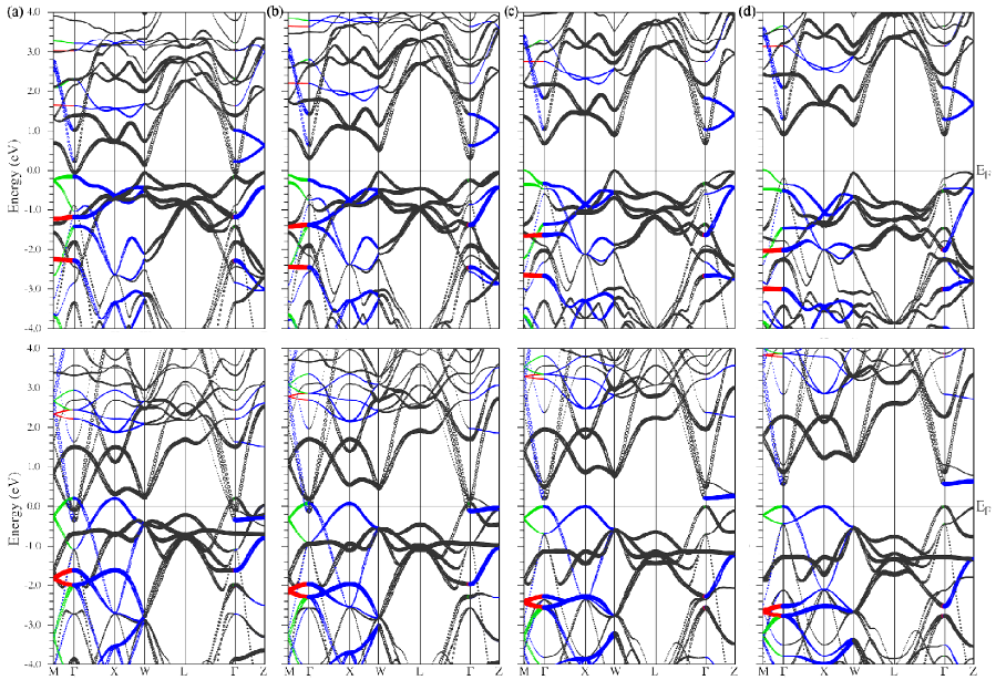
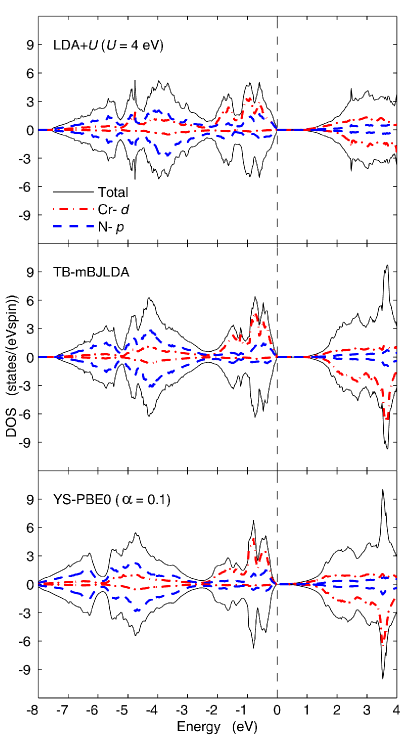
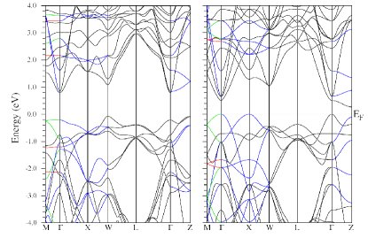
The evolution of the band structure with the value for both the cubic AFM1 and orthorhombic AFM2 phases can be seen in Fig. 2. We use an orthorhombic Brillouin zone in all cases and the following k-path: (, 0, 0)-(0, 0, 0)-(0, , 0)-(, , 0)-(0, , )--(0, 0, ). In Fig. 3, the density of states (DOS) for the orthorhombic AFM2 phase (for eV) is also shown.
For both magnetic configurations, the rough ionic electronic structure described above for the majority spin state of Cr atoms can be easily distinguished: the manifold is filled (in the range between and 0 eV below the Fermi energy), while only a small amount of (bonding) levels (in the range between and eV and hybridizing with the N orbitals) are occupied. As can be seen in Fig. 3, the band gap character is clearly - (-) although some rather small contribution of N states is also observed. Hence, CrN can be better described as a Mott-Hubbard insulator than as a charge-transfer insulator.Zaanen et al. (1985)
For the AFM2 configuration (upper panels of Fig. 2), it can be seen how for the lowest value, the band structure remains metallic with a gap opening already for eV. The unoccupied bands move up gradually as U increases. This is particularly noticeable for the first unoccupied band at for eV and also the one that forms the small electron pocket. Also, as U increases, the bands right below the Fermi level move down in energy. For larger , the Cr character near is reduced since the Cr states are shifted down in energy. The splitting between the first two bands right below the Fermi energy decreases at with increasing , increases at and causing in principle a displacement of the top of the valence band from for lower values to for higher ones (for eV, almost the same eigenvalue is obtained at and ). Some features of the band structure are U-independent: the conduction band minimum is always at and the existence of degenerate bands at which is not accidental but symmetry required.
Another observation that can be made by looking at the changes in the DOS, is a decrease of the distance between the main peaks of the occupied Cr and N bands. For eV, the distance is approximately 4 eV, while for eV it is reduced to about 2.5 eV.
Previous band structure calculations Herwadkar and Lambrecht (2009) reported that when the gap first opens at low , the top of the valence band (VBM) is at moving to as increases. Figure 4 shows the LDA+ band structure along the path (, 0, 0)- (, , 0)- (, , )- (, , 0). Our calculations show that when the gap opens (at eV), the VBM is not at but displaced to a non-high symmetry point in the direction from to , and then moving to at eV.
For the cubic AFM1 phase, a small gap of 0.20 eV is opened for eV becoming 0.56 eV for eV. We can see this evolution in the lower panels of Fig. 2. In addition, numerous degenerate bands can be seen at and (with these degeneracies clearly lifted in the orthorhombic AFM2 phase).
III.2 TB-mBJLDA electronic structure analysis
As mentioned above, the band gap values obtained for TB-mBJLDA are rather similar to those obtained from LDA+ with eV (Bhobe et al.Bhobe et al. (2010) determined an experimental value of of about 4.5 eV by PES).
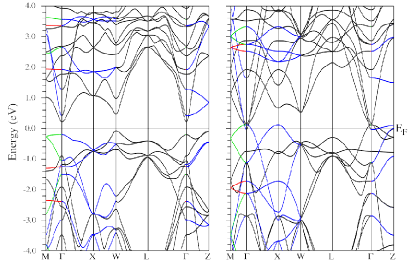
For the cubic AFM1 configuration, the band structure plot is shown in Fig. 5 (right panel). Below the Fermi level it is fairly different from the one obtained within LDA+ (with low ). In addition, the first band above the Fermi level at in LDA+ calculations lies lower in energy than with TB-mBJLDA, but it is not just a rigid band shift, some differences are noticeable particularly around the point. Actually, the bottom of the conduction band in TB-mBJLDA is no longer at but displaced to . In addition, the band gap character changes from LDA+ results being in this case a - band gap.
For the orthorhombic AFM2 phase, the splitting at between the first two bands above the Fermi level is reduced in TB-mBJLDA (see left panel of Fig. 5). The band structure obtained below the Fermi energy is very similar to the one obtained from LDA+ with eV. In addition, as for LDA+ calculations with the values of 3 to 4 eV, the VBM is not at but displaced to a non-high symmmetry point in the direction . In Fig. 3 we can compare the DOS calculated from LDA+ and TB-mBJLDA. We can see that the N character in the Cr band (from to 0 eV) is smaller in TB-mBJLDA than in LDA+ (and the opposite is true for the Cr character in the N bands below -3 eV). This effect has to do with the different hybridizations obtained with the two schemes (enhanced with the LDA+U method). In addition, the separation of N and Cr bands is larger in TB-mBJLDA, although the total valence band width is almost the same ( eV)
The optical transmission and reflection spectra of CrN are shown in Ref. Anderson et al., 2005. A band-gap-like optical transmission feature is found at 0.7 eV suggesting that CrN is a semiconductor with an indirect gap of approximately 0.7 eV and a -valley gap greater than 0.7 eV. The values of the band gap (indirect) obtained from LDA+ ( eV) and TB-mBJLDA calculations for the AFM2 phase are very close to this 0.7 eV value (0.68 eV and 0.79 eV, respectively). A gap at of about 1 eV ( eV) is also found in our calculations.
Thus, TB-mBJLDA is able to reproduce some of the effects on the electronic structure caused by the on-site Coulomb repulsion between Cr electrons without using a tunable parameter and being consistent with the results found for bulk CrN stoichiometric samples.
III.3 Hybrid functionals electronic structure analysis
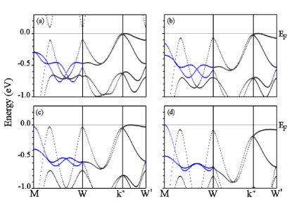
As can be seen from Table 1, the results with hybrid functionals strongly depend on the amount of HF exchange . If we take as a reference the values obtained within TB-mBJLDA (similar to those from LDA+ with eV), using gives closer results than using . The band structure for the cubic AFM1 and orthorhombic AFM2 phase are shown in Fig. 6 for the screened YS-PBE0 functional with .
For the ground state orthorhombic AFM2 phase, there is a reduction of the band gap with respect to LDA+ or TB-mBJLDA (as a consequence of the reduction of ) to 0.2 eV. The band structures retain the same features that we discussed above for LDA+ or TB-mBJLDA. In particular, the VBM is also not at , but displaced to a non-high symmetry point (see Fig. 4 for LDA+). Above the Fermi level, the splittings between the bands show more similarities with those obtained from LDA+ with eV. Figure 3 shows that the shape of the DOS is very similar to the TB-mBJLDA DOS, but the total valence band width is increased to about 8.2 eV. The same thing can be observed for the AFM1 phase: the band structure below the Fermi energy is more similar to the one obtained with TB-mBJLDA and above to that obtained with LDA+.
Hence, hybrid functionals can also describe accurately the electronic structure of CrN, but by tuning the amount of HF exact exchange. Although results and tunability with hybrid functionals are comparable with LDA+, this last method allows an easier physical description of the tuning parameter and is computationally less expensive.
IV Discussion
As can be seen from the values of the band gap in Table 1, the tendency towards a band gap opening is strongest for the AFM2 ground state phase (for LDA+ with as low as 3 eV, TB-mBJLDA, and hybrid functionals). Although more difficult, it is also possible to open a gap in the other AFM ordering (AFM1).
As mentioned in Sec. I, the intrinsic mechanism of electronic transport in CrN is a controversial issue. Most of the discrepancies in experimental works appear among those where the properties of thin films (where by epitaxial constraints even the phase transition can be suppressed) have been measured. Hence, we will focus in the couple of works where bulk polycrystalline samples have been studied to reconcile our results with previous data.Bhobe et al. (2010); Quintela et al. (2010)
In the work by Quintela et al.Quintela et al. (2010) the resistivity of Cr1-xVxN has been measured. Negative temperature coefficient of resistivity (), typical for semiconducting behavior, was observed for samples with V doping . For the system shows a positive TCR pointing to an itinerant electron behavior. Stoichiometric CrN exhibits (nonitinerant) over the whole -range although only for the behavior can be fitted to that of an activated semiconductor with a value of the activation energy of 75 meV. In the low-temperature AFM orthorhombic phase, the mechanism of electronic transport is not fully understood: neither a simple thermal activation nor a variable range hopping behavior describe the resistivity under TN. In a system with a charge gap, given the exponential dependence of with , should diverge as . However, for CrN, it goes to zero as . Hence, despite the negative TCR, CrN cannot be classified as a typical thermally activated semiconductor. The different semiconducting behavior in the low- phase was ascribed to the changes in chemical bond linked to the AFM order. Deriving the same result for stoichiometric CrN, Bhobe et al.Bhobe et al. (2010) concluded that the low temperature phase of CrN is one of the rare examples of AFM-itinerant (metallic) systems in spite of negative TCR. Back to Ref. Quintela et al., 2010, for in the Cr1-xVxN series, there is a sudden change in the sign of TCR at the Néel temperature: (itinerant) for the high- PM phase and (nonitinerant) for the low- AFM phase. Hence, it seems that for , the opening of a charge gap at the magnetic ordering temperature increases the activation energy, recovering semiconducting like behavior below .
The fact that the opening of a charge gap is intrinsic to the ground-state AFM ordering is consistent with our calculations. We show that the onset of magnetism should be accompanied of a gap opening. The behavior of the transport properties in the PM phase is beyond the scope of this work, but our calculations can conclude that the AFM phase is always insulating and, if it is not, then it has to do with issues caused by nanostructuring such as non-stoichiometries, strain, surface effects, etc. In a system situated close to a metal-insulator transition, small changes can induce a transition from localized to itinerant behavior, but this is not reachable in bulk-stoichiometric CrN in the magnetic phase, as our calculations show.
Further evidence of the existence of an unconventional electronic state in the AFM phase of CrN, not thermally activated neither fully itinerant, was observed in Ref. Quintela et al., 2010 comparing the behavior of the electrical resistivity with the thermoelectric power measurements. For stoichiometric CrN, the thermoelectric power shows linear temperature dependence (typical for metals or highly degenerate semiconductors). In addition, no discontinuity is observed at , where TCR changed from negative to positive at low temperatures.
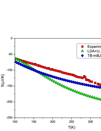
In order to check if the experimental behavior of the thermoelectric power can be reproduced from our calculations, we have obtained its dependence with temperature in the magnetic ground state (AFM2) for LDA+ ( eV) and TB-mBJLDA calculations. This has been carried out from our band structure calculations within a semiclassical approach based on the Boltzmann transport theory through the BoltzTraP code.Madsen and Singh (2006)
For the sake of comparison, we present the calculations together with the experimental values of the Seebeck coefficient taken from Ref. Quintela et al., 2010 (see Fig. 7). The results for the AFM2 phase fit the experimental values rather well, particularly in TB-mBJLDA, both in order of magnitude of the thermopower and also on the observed evolution with temperature () (although the behavior found from the calculations is not as linear as obtained experimentally).
Hence, our thermopower calculations confirm that stoichiometric CrN in the magnetic phase is semiconducting, but close to a transition from localized to itinerant electronic behavior.
V SUMMARY AND CONCLUSIONS
We have performed electronic structure calculations for CrN using a diverse set of exchange-correlation potentials: PBE, LDA+, the semilocal functional developed by Tran and Blaha based on a modification of the Becke Johnson potential,Becke and Johnson (2006) and hybrid functionals both in screened (YS-PBE0) and unscreened (PBE0) modes.
In any case, our calculations show that the onset of magnetism in CrN should be accompanied of a gap opening. We can conclude that the AFM phase is always insulating in agreement with experiments in stoichiometric bulk samples. The different metallic behavior found in various thin films has to do with nanostructuring that could include vacancies, strain, surface effects, etc. In a system situated so close to the itinerant boundary, small changes can yield metallicity and even the suppression of the magnetic transition (which we have seen from our calculations it is strongly dependent on the structural details). The behavior obtained for the thermoelectric power confirms that stoichiometric CrN in the magnetic phase is semiconducting, but close to the transition from localized to itinerant behavior. The solution we found as ground state can describe accurately the transport properties of the system.
In addition, our results give further evidence that the TB-mBJLDA functional is very useful for treating the electronic structure of correlated semiconductors giving almost the same band gaps as obtained from LDA+ with eV (close to the one determined experimentally) for different magnetic configurations allowing a parameter free description of the system. Hybrid functionals are also well capable of describing the electronic structure of CrN by tuning the amount of HF exact exchange. However, results and tunability are comparable with LDA+, that allows an easier physical description of the tuning parameter .
Acknowledgements.
The authors thank the CESGA (Centro de Supercomputación de Galicia) for the computing facilities and the Ministerio de Educación y Ciencia (MEC) for the financial support through the project MAT2009-08165. Authors also thank the Xunta de Galicia for the project INCITE08PXIB236053PR. A. S. Botana thanks MEC for a FPU grant. V. Pardo thanks the Spanish Government for financial support through the Ramón y Cajal Program. F. Tran and P. Blaha thank the Austrian Science Fund for financial support (Project No. SFB-F41, ViCoM).References
- Niewa and DiSalvo (1998) R. Niewa and F. J. DiSalvo, Chem. Mater. 10, 2733 (1998).
- Zhao et al. (1984) B. R. Zhao, L. Chen, H. L. Luo, M. D. Jack, and D. P. Mullin, Phys. Rev. B 29, 6198 (1984).
- Chockalingam et al. (2009) S. P. Chockalingam, M. Chand, A. Kamlapure, J. Jesudasan, A. Mishra, V. Tripathi, and P. Raychaudhuri, Phys. Rev. B 79, 094509 (2009).
- Lascialfari et al. (2009) A. Lascialfari, A. Rigamonti, E. Bernardi, M. Corti, A. Gauzzi, and J. C. Villegier, Phys. Rev. B 80, 104505 (2009).
- Baturina et al. (2007) T. I. Baturina, A. Y. Mironov, V. M. Vinokur, M. R. Baklanov, and C. Strunk, Phys. Rev. Lett. 99, 257003 (2007).
- Corliss et al. (1960) L. M. Corliss, N. Elliott, and J. M. Hastings, Phys. Rev. 117, 929 (1960).
- Constantin et al. (2004) C. Constantin, M. B. Haider, D. Ingram, and A. R. Smith, Appl. Phys. Lett. 85, 6371 (2004).
- Quintela et al. (2009) C. X. Quintela, F. Rivadulla, and J. Rivas, Appl. Phys. Lett. 94, 152103 (2009).
- Quintela et al. (2010) C. X. Quintela, F. Rivadulla, and J. Rivas, Phys. Rev. B 82, 245201 (2010).
- Bhobe et al. (2010) P. A. Bhobe, A. Chainani, M. Taguchi, T. Takeuchi, R. Eguchi, M. Matsunami, K. Ishizaka, Y. Takata, M. Oura, Y. Senba, et al., Phys. Rev. Lett. 104, 236404 (2010).
- Ibberson and Cywinski (1992) R. M. Ibberson and R. Cywinski, Physica B 180-181, 329 (1992).
- Filippetti et al. (1999) A. Filippetti, W. E. Pickett, and B. M. Klein, Phys. Rev. B 59, 7043 (1999).
- Filippetti and Hill (2000) A. Filippetti and N. A. Hill, Phys. Rev. Lett. 85, 5166 (2000).
- Gall et al. (2002a) D. Gall, C.-S. Shin, R. T. Haasch, I. Petrov, and J. E. Greene, J. Appl. Phys. 91, 5882 (2002a).
- Inumaru et al. (2007) K. Inumaru, K. Koyama, N. Imo-oka, and S. Yamanaka, Phys. Rev. B 75, 054416 (2007).
- Zhang et al. (2011a) X. Y. Zhang, J. S. Chawla, R. P. Deng, and D. Gall, Phys. Rev. B 84, 073101 (2011a).
- Anderson et al. (2005) P. A. Anderson, R. J. Kinsey, S. M. Durbin, A. Markwitz, V. J. Kennedy, A. Asadov, W. Gao, and R. J. Reeves, J. Appl. Phys. 98, 043903 (2005).
- Gall et al. (2002b) D. Gall, C.-S. Shin, T. Spila, M. Odén, M. J. H. Senna, J. E. Greene, and I. Petrov, J. Appl. Phys. 91, 3589 (2002b).
- Zhang et al. (2011b) X. Y. Zhang, J. S. Chawla, B. M. Howe, and D. Gall, Phys. Rev. B 83, 165205 (2011b).
- Tsuchiya et al. (1996) Y. Tsuchiya, K. Kosuge, Y. Ikeda, T. Shigematsu, S. Yamaguchi, and N. Nakayama, Mater. Trans., JIM 37, 121 (1996).
- Browne et al. (1970) J. D. Browne, P. R. Liddell, R. Street, and T. Mills, Phys. Status Solidi A 1, 715 (1970).
- Herle et al. (1997) P. S. Herle, M. S. Hedge, N. Y. Vasathacharya, S. Philip, M. V. R. Rao, and T. Sripathi, J. Solid State Chem. 134, 120 (1997).
- Rivadulla et al. (2009) F. Rivadulla, M. Bañobre-López, C. X. Quintela, A. Piñeiro, V. Pardo, D. Baldomir, M. A. López-Quintela, J. Rivas, C. A. Ramos, H. Salva, et al., Nat. Mater. 8, 947 (2009).
- Zhang and Gall (2010) X. Y. Zhang and D. Gall, Phys. Rev. B 82, 045116 (2010).
- Liechtenstein et al. (1995) A. I. Liechtenstein, V. I. Anisimov, and J. Zaanen, Phys. Rev. B 52, R5467 (1995).
- Herwadkar and Lambrecht (2009) A. Herwadkar and W. R. L. Lambrecht, Phys. Rev. B 79, 035125 (2009).
- Blaha et al. (2001) P. Blaha, K. Schwarz, G. K. H. Madsen, D. Kvasnicka, and J. Luitz, WIEN2k, An Augmented Plane Wave Plus Local Orbitals Program for Calculating Crystal Properties. ISBN 3-9501031-1-2, Vienna University of Technology, Austria (2001).
- Schwarz and Blaha (2003) K. Schwarz and P. Blaha, Comp. Mat. Sci. 28, 259 (2003).
- Hohenberg and Kohn (1964) P. Hohenberg and W. Kohn, Phys. Rev. 136, B864 (1964).
- Kohn and Sham (1965) W. Kohn and L. J. Sham, Phys. Rev. 140, A1133 (1965).
- Jones and Gunnarsson (1989) R. O. Jones and O. Gunnarsson, Rev. Mod. Phys. 61, 689 (1989).
- Sjöstedt et al. (2000) E. Sjöstedt, L. Nordström, and D. J. Singh, Solid State Commun. 114, 15 (2000).
- Madsen and Singh (2006) G. K. H. Madsen and D. J. Singh, Comp. Phys. Commun. 175, 67 (2006).
- Perdew et al. (1996) J. P. Perdew, K. Burke, and M. Ernzerhof, Phys. Rev. Lett. 77, 3865 (1996), 78, 1396(E) (1997).
- Becke and Johnson (2006) A. D. Becke and E. R. Johnson, J. Chem. Phys. 124, 221101 (2006).
- Tran and Blaha (2009) F. Tran and P. Blaha, Phys. Rev. Lett. 102, 226401 (2009).
- Singh (2010) D. J. Singh, Phys. Rev. B 82, 205102 (2010).
- Seidl et al. (1996) A. Seidl, A. Görling, P. Vogl, J. A. Majewski, and M. Levy, Phys. Rev. B 53, 3764 (1996).
- Becke (1993) A. D. Becke, J. Chem. Phys. 98, 1372 (1993).
- Czyżyk and Sawatzky (1994) M. T. Czyżyk and G. A. Sawatzky, Phys. Rev. B 49, 14211 (1994).
- Muscat et al. (2001) J. Muscat, A. Wander, and N. M. Harrison, Chem. Phys. Lett. 342, 397 (2001).
- de P. R. Moreira et al. (2002) I. de P. R. Moreira, F. Illas, and R. L. Martin, Phys. Rev. B 65, 155102 (2002).
- Kudin et al. (2002) K. N. Kudin, G. E. Scuseria, and R. L. Martin, Phys. Rev. Lett. 89, 266402 (2002).
- Ernzerhof and Scuseria (1999) M. Ernzerhof and G. E. Scuseria, J. Chem. Phys. 110, 5029 (1999).
- Adamo and Barone (1999) C. Adamo and V. Barone, J. Chem. Phys. 110, 6158 (1999).
- Bylander and Kleinman (1990) D. M. Bylander and L. Kleinman, Phys. Rev. B 41, 7868 (1990).
- Heyd et al. (2003) J. Heyd, G. E. Scuseria, and M. Ernzerhof, J. Chem. Phys. 118, 8207 (2003), 124, 219906 (2006).
- Heyd and Scuseria (2004) J. Heyd and G. E. Scuseria, J. Chem. Phys. 120, 7274 (2004).
- Tran and Blaha (2011) F. Tran and P. Blaha, Phys. Rev. B 83, 235118 (2011).
- Koller et al. (2011) D. Koller, F. Tran, and P. Blaha, Phys. Rev. B 83, 195134 (2011).
- Zaanen et al. (1985) J. Zaanen, G. A. Sawatzky, and J. W. Allen, Phys. Rev. Lett. 55, 418 (1985).