Geant4 Simulation of a filtered X-ray Source for Radiation Damage Studies
M. Guthoff, O. Brovchenko, W. de Boer, A. Dierlamm, T. Müller, A. Ritter111Now at Max-Planck-Institut für Physik, Halbleiterlabor, Otto-Hahn-Ring 6, D-81739 München, Germany., M. Schmanau, H.-J. Simonis
Institut für Experimentelle Kernphysik, Karlsruhe Institute of Technology, Campus Süd,
P.O. Box 6980, 76128 Karlsruhe, Germany
Abstract
Geant4 low energy extensions have been used to simulate the X-ray spectra of industrial X-ray tubes with filters for removing the uncertain low energy part of the spectrum in a controlled way. The results are compared with precisely measured X-ray spectra using a silicon drift detector. Furthermore, this paper shows how the different dose rates in silicon and silicon dioxide layers of an electronic device can be deduced from the simulations.
1 Introduction
Radiation hardness of semiconductors can be tested by irradiation with X-rays, since these introduce efficiently trapped ionization in the silicon oxide layers, which e.g. leads to voltage shifts in MOSFET transistors. The damage depends not only on the X-ray flux, but also strongly on the spectrum of the X-rays. The total flux can be obtained from a calibrated pin diode, but an accurate measurement of the X-ray spectrum is complex and time consuming. A simulation is a more convenient way to get the spectrum. In this paper Geant4[1] low energy extensions have been tested for this purpose. The results are compared with precisely measured X-ray spectra using a silicon drift detector (SDD). Furthermore, the different dose rates in silicon and silicon dioxide layers of an electronic device can be deduced from the simulations.
2 Experimental Setup
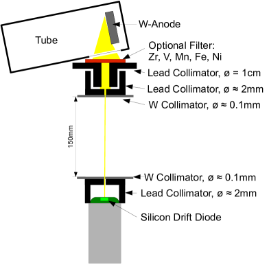
The X-ray tube of type DX-W8x0.4-2S with a tungsten anode has a maximum power of 2000 W and a maximum voltage of 60 kV. The tube window is made of 0.4 mm Beryllium, so that only low energy photons are absorbed by the window. The X-ray tube is equipped with different filters that can be mounted behind the exit window. These filters are vanadium (15 m), manganese (25 m), iron (15 m), nickel (15 m) and zirconium (75 m). These filters absorb low energy photons in different energy regions. The minimal configurable current of the HV-module is 2 mA. The top part of Fig. 1 shows the tube with the filters. The tungsten collimator for measuring the spectrum at a reduced rate in a silicon drift detector is shown in the lower part.
3 Dosimetry
One critical information in the test for radiation hardness of semiconductor devices is the dose. This chapter describes the way of calculating the dose to any kind of material if the X-ray spectrum and a reference measurement are known.
3.1 Dose rate calculated from X-ray spectrum.
The X-ray energy spectrum provided by the source is given as which can be either measured or simulated. Since obtaining a flux normalized spectrum is even more difficult, is arbitrary scaled. Only a fraction of the spectrum is absorbed during irradiation. The absorbed part is determined by:
| (1) |
where represents the density, the absorption coefficient and the thickness of the material. The absorbed power can be calculated to:
| (2) |
where represents the unknown scaling factor. The dose rate is defined as:
| (3) |
3.2 Absorbed dose in a depleted diode as reference
The missing parameter can be obtained with a reference measurement. With a depleted silicon diode it is possible to measure the photo current from ionizing radiation. Each generated electron-hole pair represents [2], so that the absorbed power in the device can be calculated as:
| (4) |
where denotes the elementary charge.
The dose rate in this device is then given by
| (5) |
where is the mass of the diode. The measured dose rate is only valid for silicon material of the same thickness. In our measurements we used a planar diode with a thickness of and a lead collimator with a circular opening of . Depletion over the whole thickness was ensured via a CV-measurement.
Using Eqs. 2 and 4 one can now obtain :
| (6) |
where is the absorbed spectrum in the reference diode. It is now possible to calculate the dose for any other material if the energy spectrum of the X-ray source is known. The spectrum can either be measured or simulated. Both ways and a comparison are described in Sect. 4.
| 29Cu | 47Ag | 56Ba | 65Tb | 241Am | ||||
|---|---|---|---|---|---|---|---|---|
| Irel | E[keV] | Irel | E[keV] | Irel | E[keV] | Irel | E[keV] | E[keV] |
| 100 | 8.048 | 100 | 22.162 | 100 | 32.193 | 100 | 44.481 | 59.5 |
| 52 | 8.028 | 53 | 21.990 | 54 | 31.817 | 56 | 43.744 | 13.9 |
| 17 | 8.905 | 16 | 24.942 | 18 | 36.378 | 20 | 50.382 | |
| 4 | 25.456 | 6 | 37.257 | 7 | 51.698 | |||
| 9 | 24.911 | 10 | 36.304 | 10 | 50.229 | |||
3.3 Calculation of the dose rate in a different material
Silicon dioxide is often used as an insulator in semiconductor devices, which suffers from charge build-up caused by ionizing radiation. Hence, for radiation damage studies it is important to know not only the total dose rate, but also the dose rate in different layers, which usually have different absorption coefficients. We use as an example to show the calculation of the dose rate in any material.
The absorbed power is calculated as in Eq. 2, and using Eq. 6 one obtains:
| (7) |
The ratio of the absorbed dose in the reference material and in the target material is therefore used to scale the reference measurement to the absorbed power in the target material . The dose rate in follows from Eqs. 3 and 7:
| (8) |
The number of absorbed photons, and , can be calculated from Eq. 1 using the known energy dependent absorption coefficients for each material[3]. In principle the method can be used for arbitrary materials and has been applied for all six possible filter settings.
4 X-ray spectrum
A measurement of the X-ray spectrum is often not possible, since the count rates are usually too high for detectors with a suitable energy resolution. Alternatively, the spectrum can be obtained from a simulation. In this chapter we describe both ways, simulations are done with Geant4, the measurements are done with a silicon drift detector.
4.1 Measurement of the spectrum
A silicon drift detector (SDD) with an integrated preamplifier of the type AXAS-P (KETEK GmbH, Munich, Germany) was used as detector. The signals were further amplified by a shaping amplifier and registered by a readout system Multiport II (Canberra Industries, Inc., Meriden, CT, USA) with 16384 ADC channels. All measurements were done with an X-ray energy of 60 kV and 2 mA anode current. With this configuration the photon flux in the detector was too high to detect single photon events, since the flux was several order of magnitude above the count rate for the slow drift detector. Two tungsten collimators were used to reduce the count rate. These collimators were 1 mm thick with a hole of 0.1 mm diameter.
One collimator was mounted at the exit window of the tube and another one on the detector, as shown in Fig. 1.
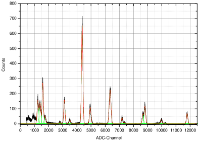
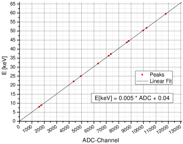
A radioactive 241Am source was used for the energy calibration. This source includes different additional materials, which are excited by the 241Am source and emit characteristic X-rays. The materials and their X-ray energies can be found in Table 1. The relation for the energy calibration is:
as obtained from a linear fit to the observed energy peaks in ADC channels, shown in Fig. 3. The small errors show that the calibration is precise.
The SDD has a thickness of 300m. Some photons pass through the detector, especially at higher energies. To compensate for this effect the absorbed spectrum was corrected by weighting it with the inverse photon absorption probability [3] for a layer of 300 m silicon. The energy resolution of the measurement was determined by fitting a Gaussian curve to the Lα peak. The full width at half maximum (FWHM) is 0.5 keV, which is comparable to the resolution 0.58 keV obtained during the energy calibration.
4.2 Geant4 simulation
Geant4 is a toolkit developed at CERN for the simulation of the passage of particles through matter [1]. It is an object-oriented simulation framework which provides a diverse set of software components [4]. All aspects of the simulation process like the geometry of the system, tracking of particles through materials and external electromagnetic fields as well as the response of sensitive detector components are included in the simulation. Geant4 provides also a set of different physics models to describe the interactions of particles with matter across a wide energy range. The standard electromagnetic physics package provides implementations of electron, positron, photon and charged hadron interactions. It is suitable for most of the Geant4 applications, but it is not optimized for low energy particles. Two specific low energy electromagnetic models are available: Livermore (based on the Livermore library [5, 6, 7]) and Penelope [8]. Geant4 version 9.3.p01 was used and the version of CLHEP libraries was 2.0.4.5. At first both low energy physics packages were used. However, results obtained with Livermore showed differences in comparison with measured spectra. The characteristic tungsten lines had a lower intensity compared to the bremsstrahlung slope. The results presented here are obtained with the Penelope package.
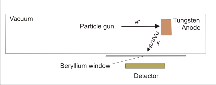
In order to reduce the simulation time the program was split into two different parts. In the first part the pure tungsten spectrum of the X-ray tube was generated. Then this spectrum was used as input for the second part, where the effect of different filters and collimators could be studied. The first step of the simulation is the generation of an electron beam with an energy of keV. The geometry is shown in Fig. 4. The environment is vacuum. The vertical position of the beam was varied by 12 mm to simulate the glow filament (the electron source within the X-ray tube). The electrons were shot at a tungsten anode at a distance of 8.5 mm. Below the anode a 0.4 mm thick beryllium window was placed. After the photons, generated at the anode, passed through the beryllium window, their energy was registered by a sensitive air layer (detector).
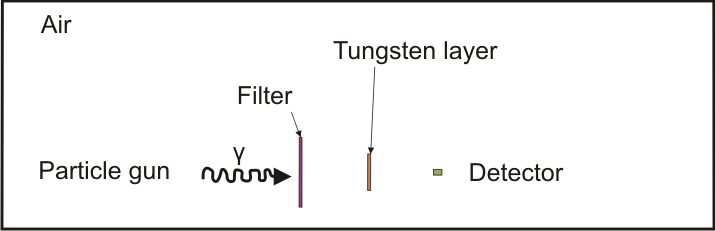
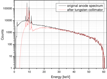
In the following step this photon spectrum was used as input for the setup shown in Fig. 5. Material and thickness of the filter were taken from the X-ray tube specifications. After the filter a tungsten collimator was used to collimate the beam. The hole geometry of this collimator is irregular, since the small hole of 0.1 mm was produced by a laser shot. The scattering on the inner edges of the two tungsten collimators was simulated by a thin tungsten foil of 3 m placed between the filter and the detector. The thickness was chosen to agree with data, as will be shown in the next section. In Fig. 6 the simulated spectra before and after this thin tungsten layer are shown.
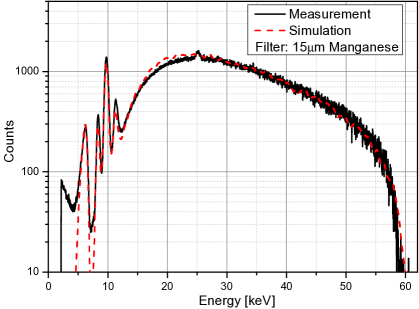
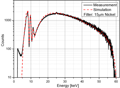
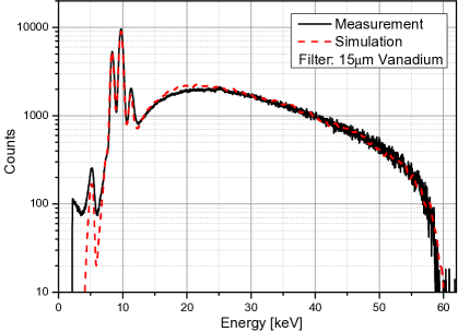
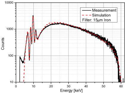
4.3 Comparison of Measurements and Simulations
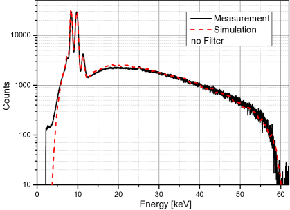
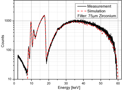
For a realistic comparison the simulations were convoluted with a Gaussian curve with the same FWHM as the detector. The measured energy spectra after all available filters are in excellent agreement with the simulations, as shown in Fig. 7. Note the reasonable agreement between simulation and measurements without filter (left top panel), which is the justification for the thin tungsten foil in Fig. 5 representing the absorption in the collimator. Only the low energy part differs slightly, which is expected, since in the simulation photons are registered, not detected by the detector. Therefore, the simulation does not include additional absorption effects in the detector, e.g. by Compton scattering. The small enhancement at 25.2 keV, which appears in every measured spectrum, is the Kα line of tin [9]. Characteristic X-ray photons from the solder used to connect the peltier cooling in the detector capsule are responsible for this peak.
5 Dose rate measurements with RadFETs
To make sure that the results are reliable we crosschecked the simulation with special ionizing radiation detectors, namely RadFETs, which consist of calibrated MOSFETs, where the shift in the threshold voltage by the positive charge build-up in the silicon oxide layer has been calibrated [10, 11]. Table 2 compares the results from the simulation with the measurements. One observes that filtering out the soft part of the spectrum (corresponding to the lower dose rates) improves the agreement between measurements and simulations, as expected since the low energy part of the spectrum in less well simulated, as discussed before.
| Filter | Dose rate | Dose rate |
|---|---|---|
| simulation | RadFETs | |
| Gy/s | Gy/s | |
| Zr | 0.24 | 0.22 |
| V | 1.84 | 1.93 |
| Mn | 0.86 | 0.90 |
| Fe | 1.32 | 1.19 |
| Ni | 1.44 | 0.99 |
| Air | 6.29 | 5.95 |
6 Summary
This paper shows a convenient method to obtain the applied dose from X-ray irradiation in the various layers of an electronic device, namely by one calibration measurement of the total flux and a simulation of the X-ray spectra, from which the dose rates in materials with different absorption coefficients can be calculated. The method has been crosschecked with calibrated RadFets. The difficult part is the reliable simulation of the X-ray spectrum after the usual filtering. We found that the Geant4 X-ray simulation with the Penelope physics package is in excellent agreement with precise measurements of the spectra using a silicon drift detector.
7 Acknowledgments
-
•
The authors would like to thank the Institute for Nuclear Physics(IK) of the Karlsruhe Institute of Technology for lending us the silicon drift detector.
-
•
We thank the KEK Institute in Japan for the support with the RadFET measurements.
-
•
We also are grateful to the German Federal Ministry of Education and Research (BMBF) for financial support.
References
- [1] “Webpage of Geant4 collaboration”. http://geant4.cern.ch, 2010.
- [2] P. Lechner, “Zur Ionisationsstatistik in Silicium”. PhD thesis, Technical University of Munich, 1998.
- [3] S. Seltzer, J. Chang, J. Coursey, R. Sukumar, M.J. Berger, J.H. Hubbell, D. Zucker, XCOM: Photon Cross Sections Database, http://www.nist.gov/physlab/data/xcom/index.cfm, 1998.
- [4] J. Allison, et al., “GEANT4 - a simulation toolkit”, NIM A 506 (2003) 250.
- [5] D. Cullen, et al., EPDL97: the Evaluated Photon Data Library, Õ97 version, UCRL-50400, vol. 6, Rev. 5, 1997.
- [6] S. Perkins et al., “Tables and graphs of electron-interaction cross-sections from 10 eV to 100 GeV derived from the LLNL evaluated electron data library (EEDL), Z=1-100”, Report UCRL-50400, Vol. 31, 1991.
- [7] S. Perkins et al., “Tables and Graphs of Atomic Subshell and Relaxation Data Derived from the LLNL Evaluated Atomic Data Library (EADL), Z=1-100”, Report UCRL-50400, Vol. 30, 1991.
- [8] F.Salvat et al., eds., “Penelope - A code system for Monte Carlo simulation of electron and photon transport”. http://www.nea.fr/dbprog/penelope.pdf, Issy-les-Moulineaux, France, November, 2001.
- [9] P. Indelicato. R.D. Deslattes, E.G. Kessler Jr. et al., “X-ray Transition Energies”. http://www.nist.gov/physlab/data/xraytrans/index.cfm, 2003.
- [10] S. Stanic, Y. Asano, H. Ishino et al., “Radiation monitoring in Mrad range using radiation-sensing field-effect transistors”, NIM A 545 (2005) 252.
- [11] L. Ruckman, G. Varner, S. Stanie et al., “Development and Implementation of a Readout Module for Radiation-Sensing Field-Effect Transistors”, IEEE Transactions 53 (2006) 2452.