Strain relaxation by dislocation glide in ZnO/ZnMgO core-shell nanowires
Abstract
Plastic relaxation of the misfit stress in core-shell semi-conducting nanowires can lead to structural defects, detrimental to applications. Core-shell ZnMgO/ZnO quantum well heterostructures were deposited on ZnO nanowires. Strain along the a and c axes of the wurtzite structure is relaxed through the glide of dislocation half-loops from the free surfaces, within pyramidal and prismatic planes. Some half-loops are closed up in the barriers to accommodate the misfit at two consecutive interfaces of the quantum well stack. Dislocations are also observed within the nanowire core: contrary to two-dimensional structures, both the core and the shell can be plastically relaxed.
Due to their particular properties, semi-conducting nanowires are widely studied for nanoelectronicsHuang et al. (2001) and optoelectronics.Huang, Duan, and Lieber (2005) The core-shell configuration is especially interesting for various applications such as transistors made of silicon and germanium,Lauhon et al. (2002) solar cells made of a ZnO core and a ZnSe shell,Wang et al. (2008) or light-emitting diodes with GaN/InGaN core-shell quantum wells.Bavencove et al. (2011) Although the core-shell structures described in most of the published works are coherently strained,Kavanagh (2010) the stress due to the lattice mismatch between the core and the shell materials may plastically relax if thicknesses and/or alloy concentrations exceed some critical values. This leads to the formation of misfit dislocations which are detrimental to device efficiencies. For example, it was demonstrated that internal quantum efficiencies of ZnO core-shell quantum wells could vary from 1 to 54% depending on the presence or not of dislocations,Thierry et al. (2012) and that InAs/GaAs core-shell nanowires containing dislocations had a reduced electron field-effect mobility compared to bare InAs nanowires.Kavanagh et al. (2011) It is therefore important to understand, and control, the strain relaxation mechanisms.
Strain relaxation in cubic two-dimensional (2D) heterostructures has been considered decades ago: it usually occurs by introducing misfit dislocations at the heterostructure interface, either by bending of pre-existing dislocations, or through the glide of dislocation half-loops from the free surface, generally on the densest atomic planes.Matthews and Blakeslee (1974, 1975) Similar mechanisms are at play when strain relaxation occurs through dislocations in hexagonal compact 2D heterostructures. For c oriented growth, glide occurs in pyramidal planes, because the dense basal and prismatic planes are not active glide systems.Srinivasan et al. (2003); Floro et al. (2004) For m plane growth, glide can occur on prismatic planes,Yoshida et al. (2011) and for semipolar plane growth, glide can occur on both basal and prismatic planes.Wu et al. (2011a) Concerning relaxation in nanowire core-shell structures, theoretical studies have been published.Ovid’ko and Sheinerman (2004); Raychaudhuri and Yu (2006); Trammell et al. (2008) Strain energies have been calculated for cubicTrammell et al. (2008) and wurtziteRaychaudhuri and Yu (2006) structures. For wurtzite materials, the strain energy was compared to the dislocation energy in order to determine the critical thickness for plastic relaxation. The role of the shell thickness and composition was shown, similarly to the 2D case, but the core thickness has also an influence because both the core and the shell are stressed and store a part of the strain energy.Raychaudhuri and Yu (2006) Numerical evaluation of the critical thicknesses was made for nitride materials. In these models, edge misfit dislocations were assumed to be formed by glide and climb.Ovid’ko and Sheinerman (2004) Concerning experimental observations, edge misfit dislocations were observed at the interface of wurtzite InAs/GaAs core-shell nanowires.Popovitz-Biro et al. (2011); Kavanagh et al. (2012) However, there are no indications of dislocations threading from the InAs/GaAs interface to the surface, which made more difficult discussing the glide systems. Concerning ZnO/ZnMgO core-shell nanowires we have shown that structures with ZnMgO barriers on ZnO were elastically strained, contrary to structures with ZnMgO barriers, which were plastically relaxed because of a twice higher lattice mismatch.Thierry et al. (2012) The type of the formed dislocations was not addressed for ZnO/ZnMgO, and the glide systems were addressed neither for InAs/GaAs nor for ZnO/ZnMgO.
In this work, we first analyze the possible glide systems for dislocations in core-shell nanowires with the wurtzite structure. Then, the dislocations caused by plastic relaxation are experimentally observed in a system composed of a ZnO core, and of a heterostructure shell consisting in four ZnMgO barriers and three ZnO quantum wells. It is shown that the misfit strain is relaxed through the glide of dislocation half-loops from the surface in prismatic and pyramidal planes. Some loops are closed because of the presence of alternated ZnMgO and ZnO shell layers. Finally, a few dislocations are also observed in the ZnO core, showing that both the shell and the core relax to accommodate the strain.
ZnO nanowires were grown on sapphire by metal organic vapor phase epitaxy: details about the growth can be found in a previous publication.Rosina et al. (2009) The nanowires grew vertically along the +c direction, without any structural defects such as stacking faults or dislocations.Perillat-Merceroz et al. (2010, 2012) ZnO core-shell multi-quantum wells were subsequently grown radially on the ZnO nanowires. The heterostructure consists in three 4 nm-thick ZnO quantum wells within 10 nm-thick ZnMgO barriers.Thierry et al. (2012) The lattice mismatch between ZnMgO and ZnO is +0.6% along a, -0.7% along c, and ZnMgO was shown to be of wurtzite structure up to x=0.33.Ohtomo et al. (1998) In our case with x=0.3, it is thus expected that ZnMgO keep the wurtzite structure. Electron diffraction patterns showed only one set of spots corresponding to the wurtzite phase for the ZnO/ZnMgO heterostructure, because the misfit between ZnO and ZnMgO is too small to distinguish separated spots for the two materials. Transmission electron microscopy (TEM) images were taken on a FEI-Tecnai microscope operated at 200 kV. TEM samples were prepared by the cleaved edge method for cross sections, and by focused ion beam for plan views. Details about the growth conditions and TEM sample preparation can be found in Ref.Thierry et al. (2012). The , , and directions of the hexagonal compact structure are noted c, a, and p respectively. The basal plane is refered as the c plane, while the prismatic planes and are the a and m planes respectively. In the hexagonal compact structure, the more common dislocations are either perfect ones, with Burgers vector b equal to a, c, or a+c, and partial ones with b equal to p, 2p, c/2, c+2p, c/2+p, or c+p.Hirth and Lothe (1982)
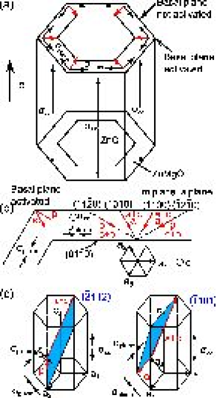
Before describing our observations of dislocations due to plastic relaxation, let us examine what the activated glide systems could be for dislocations in wurtzite core-shell nanowires with m-plane facets. The stress state of a wurtzite nanowire consisting of a ZnO core and a ZnMgO barrier is presented in figure 1 (a). The actual sample studied here is more complicated, with a stack of four ZnO quantum wells and three ZnMgO barriers grown on a ZnO core. However, in a first approach, this stack can be approximated by a unique ZnMgO barrier with an average Mg content lower than the four ZnMgO barriers. ZnMgO has a c parameter smaller than ZnO, and a larger a parameter.Ohtomo et al. (1998) This lattice mismatch induces a tensile stress in the ZnMgO shell along the c direction, and a compressive stress in the a direction, for each m facet of the nanowire. Consequently, at the corner between two facets, there is a component of the stress directed towards the center of the nanowire, which is not present in the case of a 2D layer grown on a m face. Figure 1 (b) represents the possible prismatic glide planes by dashed lines in a core-shell nanowire, with the activated glide directions indicated by red arrows. a and m planes can be activated by the misfit stress, with glide directions being respectively p or c+p, and a or a+c. Burgers vector can be respectively c, p or c+p, and c, a or c+a. Figure 1 (c) shows possible pyramidal glide planes and glide directions. Dislocations can glide for example in planes along p or a+c with b=p, a+c, c+2p, or c/2+p, and in planes along a or a+c with b=a or a+c. Higher index pyramidal planes could also be envisaged, but they would be energetically less favored. Because the stress is directed inwards at the corners of the nanowire, the projected stress on the prismatic and pyramidal planes is increased at these corners. Moreover, glide in the basal plane directions p and a are activated at these corners, with a Burgers vector p or a. Besides, it was observed that, for GaN/InGaN 2D heterostructures grown on semipolar planes, glide of dislocations with b=a can occur in the basal planes.Wu et al. (2011b) Consequently, the misfit dislocations with b=c/2 in a basal plane observed in GaAs/InAs core-shell nanowiresPopovitz-Biro et al. (2011); Kavanagh et al. (2012) cannot be formed by glide from the free surface. It was proposed that this type of dislocation could be formed by climb, by dislocation reaction, or by glide.Ovid’ko and Sheinerman (2004); Kavanagh et al. (2012) Glide would be possible only at the very top of the nanowires, or if the shell growth occurred by isolated islands which would coalesce.
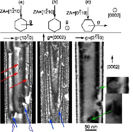
Figure 2 shows weak-beam TEM images of the same nanowire taken along the zone axis, with (a) and (b) , and (c) a two-beam image taken along the zone axis with . Different types of dislocations are visible.
First, dislocation half-loops in pyramidal planes are indicated by blue arrows on the and images. Their shape is outlined in blue for more clarity. One must keep in mind that TEM images are 2D projections of the whole nanowire: that is the reason why some half-loops do not continue until the apparent sides of the nanowire. For , vertical fringes may be visible in the pyramidal plane dislocations (some are indicated by green arrows). This fringes are a moiré caused by a stacking fault inside the dislocation half-loop. However, stacking faults caused by the glide of common partial dislocations in the wurtzite structure (p, 2p, c/2, c+2p, c/2+p, c+p) are extinguished with , according to the criterion which states that stacking faults are not visible if is a multiple of (with the displacement vector of the stacking fault). Furthermore, prismatic stacking faults with have been observed in the wurtzite structure, and give a contrast for .Drum (1965) These prismatic stacking faults intersected basal ones with , and thus stair-rod dislocations with b=p/2 were present at the intersections. We speculate that the dislocations observed here may have a non classical Burgers vector component in the basal plane such as b=p/2, which gives a stacking fault contrast with . Because these dislocations are visible for and , their Burgers vector b has not only a component in the basal plane, but also a component along c. Consequently, they release the misfit strain both along a and along c. It is worth noting that the major part of the dislocations is threading to the surface, whereas the portion of the dislocations at the interface (the so-called "misfit dislocations") is relatively shorter. This is in contrast with the observations in InAs/GaAs nanowires where supplementary half-planes due to large misfit dislocations were visible on high resolution TEM images.Popovitz-Biro et al. (2011); Kavanagh et al. (2012) This difference could be due to the different values of misfit: 0.6% for ZnO/ZnMgO, and 6.8% for InAs/GaAs, along a. Moreover, it was shown that some inclined threading dislocations do play a role in the strain relaxation.Cantu et al. (2005)
Second, dislocation half-loops in planes which give a contrast along a vertical line on the image with are indicated by red arrows. Considering perfect dislocations, the three possibilities for the Burgers vector for a dislocation gliding in the plane are , , and . Because the dislocations are not visible for , they should be , according to the simplified extinction criterion which states that a dislocation is not visible when . However, a dislocation with should neither be visible with . Besides, they are not visible on the bright field image taken with (not shown here). The contrast on the weak-beam image could be a residual contrast because the term is not equal to zero for and u along c. These dislocations can release misfit strain along the a direction. Concerning 2D heterostructures, it was observed for GaN/InGaN that relaxation could occur through the glide of dislocations with b=a on prismatic planes, for growth on m planeYoshida et al. (2011) and semipolar planeWu et al. (2011b). Moreover, b=a misfit dislocations were observed in InAs/GaAs core-shell nanowires.Popovitz-Biro et al. (2011)
To summarize, dislocations are observed to glide in prismatic and pyramidal planes, but not in basal planes. Consequently, the misfit along c is not released in our case by dislocations lying in basal planes, as proposed in theoretical models,Ovid’ko and Sheinerman (2004); Raychaudhuri and Yu (2006) and as observed for InAs/GaAs core-shell nanowires.Popovitz-Biro et al. (2011); Kavanagh et al. (2012) Instead, it is released by loops lying in pyramidal planes with a Burgers vector with two components, one along c, and one within the c plane. Misfit along a is released by these loops in pyramidal planes, and by loops in prismatic planes.
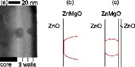
Figure 3(a) shows another TEM image of a core-shell nanowire viewed in cross-section: the ZnO core is visible on the left, and then the four ZnMgO barriers and the three ZnO quantum wells. A closed dislocation loop is observed between the ZnO core and the first ZnO quantum wells. Its formation mechanism can be explained as follows. First, a dislocation half-loop is formed in a ZnMgO barrier to accommodate the misfit with the ZnO core [Fig. 3(b)]. Then, because of the subsequent growth of a ZnO quantum well on the ZnMgO barrier, the dislocation half-loop closes up in order to accommodate the misfit between the ZnMgO barrier and the ZnO well: the same dislocation loop accommodates the misfit at the two opposite ZnO/ZnMgO interfaces [Fig. 3(c)]. A similar explanation was originally proposed for a GaAs/GaAsP 2D multiple-stack.Matthews and Blakeslee (1974)

Figure 4 shows a plan view image of a nanowire viewed along the zone axis, with an objective aperture on the direct beam. A pyramidal dislocation loop with moiré fringes, circled in red, is visible between two ZnO quantum wells: it is another example of a closed dislocation loop. Moreover, a dislocation is visible in the nanowire core. Trammell et al. showed that the strain energy was mainly stored in the shell for thin shells relative to the core, whereas this energy was mainly stored in the core for relatively thicker shells.Trammell et al. (2008) Consequently, there would be two steps for the plastic relaxation in core-shell structures. First, when the shell is thin compared to the ZnO core, plastic relaxation occurs mainly in the shell. Second, when the shell becomes thicker, the ZnO core itself may relax to accommodate the misfit strain through the generation of dislocations within it. However, the source of these dislocations is not obvious because the ZnO core is free of defects before the growth of the shell. It is worth noting that according to Raychaudhuri et al., with a thin enough core and a low enough barrier composition, the barrier can have an infinite thickness without being plastically relaxed.Raychaudhuri and Yu (2006) Our observations in Ref.Thierry et al. (2012) seems to confirm this point: for 75 nm thick barriers with 15% Mg concentration on a 60 nm core, no plastic relaxation was observed.
To conclude, we have identified plastic relaxation mechanisms in ZnO/ZnMgO core-shell nanowires. It was shown, through a contrast analysis in TEM, that strain relaxation along the c and a directions of the facets of the wurtzite core-shell nanowires occurred through the glide of dislocation half-loops from the free surface to the interface. Glide occurs in pyramidal planes, with the Burgers vectors of the dislocations having a component both along c and in the c plane, and in prismatic planes, with b=a. Some of these half-loops may close up in order to accommodate the misfit at two consecutive opposite interfaces (ZnO/ZnMgO and ZnMgO/ZnO) of the nanowire heterostructure. The stress state in these one-dimensional structures is different from 2D layers, because of the finite dimensions of the m and a facets. Actually, the presence of corners between these facets induces inhomogeneous strain fields in the shell. Another difference is the presence of dislocations within the nanowire core itself, although the formation mechanism of these dislocations remains unclear. These observations will help design optimized core-shell nanowires heterostructures, by an adequate choice of core and layer thicknesses and composition in order to avoid the formation of detrimental defects such as dislocations.
Acknowledgements.
The authors acknowledge Eric Gautier for help during the FIB preparation of TEM samples, and the French national research agency (ANR) for funding through the Carnot program (2006/2010).References
- Huang et al. (2001) Y. Huang, X. Duan, Y. Cui, L. J. Lauhon, K. Kim, and C. M. Lieber, Science 294, 1313 (2001).
- Huang, Duan, and Lieber (2005) Y. Huang, X. Duan, and C. M. Lieber, Small 1, 142 (2005).
- Lauhon et al. (2002) L. J. Lauhon, M. S. Gudiksen, D. Wang, and C. M. Lieber, Nature 420, 57 (2002).
- Wang et al. (2008) K. Wang, J. Chen, W. Zhou, Y. Zhang, Y. Yan, J. Pern, and A. Mascarenhas, Advanced Materials 20, 3248 (2008).
- Bavencove et al. (2011) A. Bavencove, D. Salomon, M. Lafossas, B. Martin, A. Dussaigne, F. Levy, B. Andre, P. Ferret, C. Durand, J. Eymery, L. S. Dang, and P. Gilet, Electronics Letters 47, 765 (2011).
- Kavanagh (2010) K. L. Kavanagh, Semiconductor Science and Technology 25, 024006 (2010).
- Thierry et al. (2012) R. Thierry, G. Perillat-Merceroz, P. H. Jouneau, P. Ferret, and G. Feuillet, Nanotechnology 23, 085705 (2012).
- Kavanagh et al. (2011) K. L. Kavanagh, J. Salfi, I. Savelyev, M. Blumin, and H. E. Ruda, Applied Physics Letters 98, 152103 (2011).
- Matthews and Blakeslee (1974) J. Matthews and A. Blakeslee, Journal of Crystal Growth 27, 118 (1974).
- Matthews and Blakeslee (1975) J. W. Matthews and A. E. Blakeslee, Journal of Crystal Growth 29, 273 (1975).
- Srinivasan et al. (2003) S. Srinivasan, L. Geng, R. Liu, F. A. Ponce, Y. Narukawa, and S. Tanaka, Applied Physics Letters 83, 5187 (2003).
- Floro et al. (2004) J. Floro, D. Follstaedt, P. Provencio, S. Hearne, and S. Lee, Journal of Applied Physics 96, 7087 (2004).
- Yoshida et al. (2011) S. Yoshida, T. Yokogawa, Y. Imai, S. Kimura, and O. Sakata, Applied Physics Letters 99, 131909 (2011).
- Wu et al. (2011a) F. Wu, E. C. Young, I. Koslow, M. T. Hardy, P. S. Hsu, A. E. Romanov, S. Nakamura, S. P. DenBaars, and J. S. Speck, Applied Physics Letters 99, 251909 (2011a).
- Ovid’ko and Sheinerman (2004) I. A. Ovid’ko and A. G. Sheinerman, Philosophical Magazine 84, 2103 (2004).
- Raychaudhuri and Yu (2006) S. Raychaudhuri and E. T. Yu, Journal of Applied Physics 99, 114308 (2006).
- Trammell et al. (2008) T. E. Trammell, X. Zhang, Y. Li, L. Chen, and E. C. Dickey, Journal of Crystal Growth 310, 3084 (2008).
- Popovitz-Biro et al. (2011) R. Popovitz-Biro, A. Kretinin, P. Von Huth, and H. Shtrikman, Crystal Growth & Design 11, 3858 (2011).
- Kavanagh et al. (2012) K. L. Kavanagh, I. Saveliev, M. Blumin, G. Swadener, and H. E. Ruda, Journal of Applied Physics 111, 044301 (2012).
- Rosina et al. (2009) M. Rosina, P. Ferret, P. Jouneau, I. Robin, F. Levy, G. Feuillet, and M. Lafossas, Microelectronics Journal 40, 242 (2009).
- Perillat-Merceroz et al. (2010) G. Perillat-Merceroz, P. H. Jouneau, G. Feuillet, R. Thierry, M. Rosina, and P. Ferret, Journal of Physics: Conference Series 209, 012034 (2010).
- Perillat-Merceroz et al. (2012) G. Perillat-Merceroz, R. Thierry, P. Jouneau, P. Ferret, and G. Feuillet, Nanotechnology 23, 125702 (2012).
- Ohtomo et al. (1998) A. Ohtomo, M. Kawasaki, T. Koida, K. Masubuchi, H. Koinuma, Y. Sakurai, Y. Yoshida, T. Yasuda, and Y. Segawa, Applied Physics Letters 72, 2466 (1998).
- Hirth and Lothe (1982) J. P. Hirth and J. Lothe, Theory of dislocations (Krieger Pub. Co., 1982).
- Wu et al. (2011b) F. Wu, A. Tyagi, E. C. Young, A. E. Romanov, K. Fujito, S. P. DenBaars, S. Nakamura, and J. S. Speck, Journal of Applied Physics 109, 033505 (2011b).
- Drum (1965) C. M. Drum, Philosophical Magazine 11, 313 (1965).
- Cantu et al. (2005) P. Cantu, F. Wu, P. Waltereit, S. Keller, A. E. Romanov, S. P. DenBaars, and J. S. Speck, Journal of Applied Physics 97, 103534 (2005).