Negative Differential Conductance in Nano-junctions: A Current Constrained Approach
Abstract
A current constrained approach is proposed to calculate negative differential conductance in molecular nano-junctions. A four-site junction is considered where a steady-state current is forced by inserting only the two central sites within the circuit. The two lateral sites (representing e.g. dangling molecular groups) do not actively participate in transport, but exchange electrons with the two main sites. These auxiliary sites allow for a variable number of electrons within the junction, while, as required by the current constrained approach, the total number of electrons in the system is kept constant. We discuss the conditions for negative differential conductance in terms of cooperativity, variability of the number of electrons in the junction, and electron correlations.
I Introduction
Understanding of charge transport through low dimensional electronic system has got tremendous impetus in recent years because of their huge potential in advanced electronic devices. Ratner ; Sanvito Especially, the possibility to switch a molecule between off and on states and to support decreasing current with increasing voltage, the so called negative differential conductance (NDC) behavior, are hot topics in the field of single molecule electronics, mainly due to its credible applications. Since its first observation in the tunnel diode by Esaki in 1958, Esaki NDC has been subject of many experimental and theoretical studies. NDC has been observed in a variety of experimental systemsTour ; Don and has been discussed theoretically, even if most of theoretical work was based on one-electron pictures. Seminario ; Cornil ; rpati ; lakshmi_PRB ; lakshmi_jpc ; Cuniberti1 ; ranjit1 Recent experiments demonstrated NDC in double quantum dots junctions Ono ; tarucha and have rekindled interest in the phenomenon, occurring in the low temperature, weak-coupling limit. Several theoretical studies on donor-acceptor double quantum dot systems address strong rectification and NDC features within many-electron pictures. Thielmann ; Hettler1 ; wegewis ; Hung ; Cuniberti ; Aghassi ; Paulsson ; Datta2 ; Datta3 ; Bhaskaran ; IEEE ; prakash However, all available theoretical studies of NDC are based on voltage constrained (VC) approaches, where the electric current is driven through the junction by imposing a finite potential drop between two applied electrodes. Two semi-infinite electronic reservoirs are unavoidably introduced in VC models, posing some fundamental problems and leading to a picture difficult to reconcile with correlated electrons. Kohn1 ; Mera ; Green
As an alternative to VC approach, current constrained (CC) approaches have been developed to describe transport in both meso- and molecular junctions. CC approaches avoid any reference to reservoirs, and quite naturally apply to correlated electrons. Kohn1 ; Mera ; Ng ; Magnus ; Kosov1 ; Kosov2 ; Burke ; Anna On physical grounds, a current can be forced in a circuit by driving a time-dependent magnetic flux through the circuit. The model, originally proposed by W. Kohn to describe optical conductivity in extended systems, Kohn2 has been applied to describe electrical transport in mesoscopic systems, Kohn1 ; Magnus and more recently in molecular junctions. Burke ; Anna Alternatively, variational techniques can be adopted, and the system can be forced in a current-carrying non-equilibrium steady state introducing properly defined Lagrange-multipliers in the Hamiltonian. While offering an interesting alternative to the popular and successful VC methods, the CC approach suffers from several limitations that hinders its widespread use.Anna Not explicitly accounting for contacts, the CC approach relies on phenomenological models for the relaxation dynamics to describe dissipation. In polyatomic junctions, constraints must be explicitly enforced to avoid charge accumulation at atomic sites within the junctions, leading to a cumbersome numerical problem for large and asymmetric molecular systems.Anna Finally, in VC approaches electrons can be exchanged between the electrodes and the molecular junction and charge injection/depletion phenomena can be observed upon changing the applied gate voltage. These phenomena are critical to many processes, including NDC, but can not be described in CC approaches where the current is forced through a closed circuit and the total number of electrons in the junctions is strictly constant.
Here we propose a simple and effective strategy to overcome the last general problem inherent to CC approach. Specifically, we demonstrate that if one or more auxiliary sites are attached to the main current-carrying nanojunction, they can exchange electrons with the junction, thus representing electron source or sink. Along these lines, we present for the first time a calculation of NDC within a CC-based model. Describing NDC in an alternative picture with respect to the widespread VC-based models deepens our current understanding of the basic physics underlying this strongly non-linear phenomenon, as required to control and optimize the performance of NDC-based devices.
II The model and method
Previous work from two of the present authors based on the VC approach demonstrated interesting nonlinear behavior in the current-voltage characteristics of two-dot systems with correlated electron. lakshmi_PRB ; lakshmi_jpc Taking clue from this work, here we explore transport behavior in two-dots junctions within the CC approach. The study becomes interesting, especially in the context of the number of electrons within the junction, which plays an important role in the low-bias current-voltage characteristics.
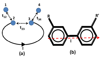
Fig. 1(a) shows a rough sketch of the model. We consider a 4 sites Hubbard model as described by the Hamiltonian:
| (1) | |||||
where () annihilates (creates) an electron with
spin on site and . For the sake of simplicity in the following
we set constant on-site repulsions, , and hopping integrals
, even if different choices have been explored. Moreover
we consider an asymmetric junction with a weak bond: , .
The eigen states of are stationary states and do not sustain any current. To induce current through the central (2-3) sites we insert these two sites into a closed circuit through which we impose a current according to the CC prescription:
| (2) |
where measures the current flowing through the bond between sites 2 and 3 (the junction region). Here and in the following and are adopted as units for charge and momentum, respectively. The field coupled to the current enters the Hamiltonian as a Lagrange multiplier, whose value is fixed by the requirement that a finite current flows through the system. The eigenstate of describe electrons with a finite overall linear momentum which looks rather unphysical in an open circuit, as described by . This paradox can be solved, according to Burke et al.,Burke connecting the two ends of the junction (sites 2 and 3 in our model system) through a long, thin and ideally conducting wire so that electrons escaping from the right side of the junction immediately appear on the left side as to maintain fixed number of electrons inside the junction. As schematically shown in Fig. 1, the junction is then inserted in a closed loop and this allows to assign a precise physical meaning to , that was introduced formally as a Lagrange multiplier. Following the seminal work of Kohn,Kohn2 in fact one can force a current through a closed ring threading an oscillating magnetic field of frequency through the center of the ring to generate a spatially uniform oscillating electric field across the junction. At the leading order in the field,maldague the Hamiltonian in the presence of a magnetic flux can be written as in Eq. 2 with proportional to the amplitude of the vector potential. Quite interestingly, a similar result has been recently reported via a general and exact projection operator technique.mukamelRMP
The two central sites (sites 2 and 3) are inserted in a closed circuit where the current is forced (cf Fig. 1a) and hence take active part in transport. The lateral sites (1 and 4) represent auxiliary sites: the current does not flow through these sites, but they are connected to the circuit and, exchanging electrons with the main sites (2 and 3), provide a source/sink for the injection/removal of electrons within the circuit. Being interested in NDC we set : the model then describes four weakly connected quantum dots. Alternatively, the same model may represent a minimal model for a molecular junction with at least one weak (poorly conjugated) bond and with two dangling groups (R and R’) connected to the current carrying skeleton as shown, as an example in Fig. 1(b). From a chemical perspective, the groups R and R’, modeled by the auxiliary sites of Fig. 1a can behave as electron withdrawing/donating groups with respect to the main sites.
If the auxiliary sites (1 and 4) are disconnected from the main circuit () the number of electrons participating in transport is strictly constant: having inserted the two central sites in an (ideal) closed circuit implies that electrons escaping from site 3 immediately enter on 2 (or viceversa). As discussed above, the obvious constraint of constant charge in a closed circuit hinders the description of phenomena related to charge injection/depletion processes, that are instead easily captured in VC approaches where electrons are exchanged between the junction and the leads. However, if the auxiliary sites are connected to the junction the number of electrons within the circuit, , becomes a variable: finite and/or allow for charge injection/depletion within the junction.
The Hubbard Hamiltonian in Eq. (1) and its current-carrying
version in Eq. (2) can be written on a real-space basis and the
resulting matrix can be diagonalized
exactly. The real space basis is defined by the
complete and orthonormal set of functions () that specify the occupation of
site spin-orbitals. Both the total number of electrons, , and the z-component of the
total spin, , commute with the Hamiltonian, and the Hamiltonian
matrix can be defined for a particular
charge and spin sector. Here we set and work in the subspace
relevant to the ground state, i.e., =0, for a grand total of 256
basis states.
The definition of characteristic current-voltage curves is quite subtle in CC approaches. As discussed above, Hamiltonian in Eq. 2 describes (at the leading order in the vector potential) the effect of an oscillating magnetic flux driving a current through a circuit. In this view, is simply proportional to the corresponding electrical field: .Kohn2 ; maldague However in the DC limit, , the driving field, and hence the driving potential vanish, leading to the unphysical result of a finite current at zero bias. This zero-resistance picture emerges because relaxation dynamics is neglected: in fact a finite potential drop is required to sustain current just to overcome friction in the junction. The calculation of characteristic curves in the CC approach then requires a model for relaxation dynamics. In particular, the current-carrying state, , is a non-equilibrium state and the system relaxes back to the ground state, . The amount of power spent to sustain the system in the non-equilibrium current-carrying state is set by the relaxation dynamics: the faster the relaxation the more power must be spent to sustain the current. The Joule law defines the relation between the electrical power spent on the molecule, , and the potential drop needed to sustain the current: . Since is known, characteristic curves can be obtained from .Anna
We adopt a simple phenomenological model for relaxation dynamics that is widely used in spectroscopy. The model is general and properly obeys basic physical requirements, including detailed balance. In particular relaxation is described by introducing the density matrix () written on the basis of the eigenstates of . On this basis the equilibrium density matrix is diagonal, with diagonal elements describing the Boltzmann populations of the relevant states. Relaxation dynamics of digonal elements of are only affected by inelastic scattering and are written as:Mukamel ; Boyd
| (3) |
where measures the probability of the transition from to as due to inelastic scattering events. Off diagonal elements of the relaxation matrix may be written as:
| (4) |
where
| (5) |
accounts for both inelastic scattering events, via the population inverse lifetimes , and for elastic scattering events via that describes the loss of coherence due to pure dephasing phenomena.Mukamel ; Boyd
The total work exchanged by the junction, , has 2 non-vanishing contributions: that represents the work done on the junction to sustain the current and a second contribution, , that measures the work dissipated by the junction. Since the current operator, , has vanishing diagonal elements on the real eigenstates of , is only affected by the relaxation of off-diagonal elements of the density matrix. As a result, both elastic and inelastic scattering events affect . This is a physically relevant result; in fact, both phenomena concur to build up the resistance in the junction. On the opposite, the power dissipated by the junction, , is only affected by inelastic scattering events. It represents just a fraction of the total power dissipated on the junction, thus suggesting that some dissipation must occur at the electrodes.Anna
While the relaxation model is fairly crude and requires invoking electrodes to actually balance the energy, it has the advantage of setting on a firm basis the relation between the molecular resistance and dissipation phenomena. In particular we notice that the proposed model properly predicts the maximum conductivity of the simplest junction as as a result of the maximum lifetime of the electron within the junction which cannot be longer than the time required to the electron to cross the junction.Anna This observation drives us to the non-trivial role of electrodes on relaxation dynamics. In the case of very weak contacts, the presence of metallic surfaces close to the molecular junction is expected to open new channel for energy dissipation then reducing the population lifetimes.lifetime On the opposite, in the strong contact regime the mixing of the discrete molecular eigenstates with the continuum of states of the metallic leads is responsible for increased dephasing rates.Datta3 A very simple model for the relaxation matrix can then be obtained in the strong contact regime, where depopulation contributions to can be neglected, and in the hypothesis that the effects of the electrodes on the dephasing rates is similar on all states, so that . In this hypothesis and the potential drop is simply proportional to : .Anna Without loss of generality we set in the following.
III Results and Discussion
We consider two different choices for the energies of the
auxiliary sites: in the first model (model a) we set =
- to mimic groups with opposite electron donating/accepting characteristics.
In the second model (model b) we set =
mimicking two equivalent side-groups added to the main
chain (R=R’ in Fig. 1(b)). Quite interestingly, the second
model can also describe the effects of charge injection/depletion in the
junction as a result of an applied gate voltage.
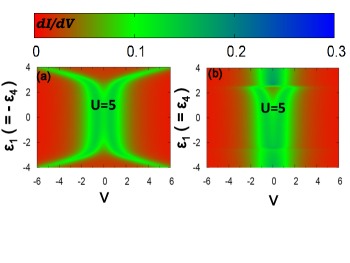
The color maps in Fig. 2 show the differential conductance () calculated as a function of the potential drop ()
and of the energies of the auxiliary sites,
(left panel) and (right panel) for .
NDC is not observed in either case.
This result, confirmed at different
values, is not surprising. In fact NDC suggests a
largely non-linear behavior of the junction, with a bistable
characteristic. Such a behavior requires cooperativity and hence the
introduction of some self-consistent interaction in the model.
With this requirement in mind, we modify the model to account for possible effects of the voltage drop on the auxiliary sites. In fact, sites 1 and 4 do not play any active role in transport, but can be affected by the voltage drop at the junction. In particular, being directly connected to sites 2 and 3 (device region), they can experience at least a portion of the electrical field required to sustain the current in the main junction. As a result, a term is added to the Hamiltonian affecting the auxiliary-site energies as follows:
| (6) |
where measures the fraction of the potential drop that is felt by sites 1 and 4. We observe that only the energy of auxiliary sites must be explicitly modified by the potential: the effect of the potential on the junction (sites 2 and 3) is already accounted for by the Hamiltonian in Eq. 2. The correction term in Eq. 6 introduces cooperativity in the model: the on-site energies, and , do depend in fact on the current flowing through the junction that, in turn is affected by the on-site energies. Color maps in Fig. 3, obtained setting show NDC regions, demonstrating the cooperative nature of the phenomenon. Fig. 3 summarizes the main results of this paper showing the differential conductance calculated for the two choices, (a) (left columns), and (b) (right columns) and 5 and 2 (top and bottom panels, respectively). NDC feature is definitely more prominent in model b than in model a and is suppressed upon decreasing electron correlation strength, (this conclusion is also supported by extensive calculations run at different ). These findings are in line with results obtained in the VC approach, showing that strong on-site correlations favor NDC in double-quantum dot systems. prakash Note that, the () map (and the characteristics as well) are asymmetric because of the inherent asymmetry in the device region, with sites 2 and 3 having different on-site energies.
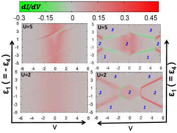
Due to symmetry reasons, the number of electrons in the junction is constant in model (a), . In model (b), is instead variable. Since the hybridization energy, , is small with respect to on-site energies, assumes almost integer and constant values (shown as italic numbers in the figures) in different regions of the plane connected by very sharp borders. Quite impressively, NDC features are observed for model (b) just at these borders, suggesting a strong relation between NDC and sharp variations of . Upon decreasing , the variation of becomes smooth and the NDC regions become less prominent. Minor NDC features are also observed in model (a) with constant , in regions where the occupancy of the two auxiliary sites abruptly changes from =0 to .
To obtain a more detailed picture of the microscopic origin of NDC, we
disentangle the contributions to the current from the different
states. Specifically we work a real-space basis, where
states are defined assigning electrons with a specified spin to
each site in the junction. A generic state then graphically represents the
state where no electrons are found in the first site, one electron
with spin and one electron with spin are located on sites 2
and 3, respectively, and site 4 is doubly occupied. In more formal
language:
where are the electron creation operators
entering the Hamiltonian in eq. 1 and is vacuum state-
The current-carrying ground state has complex coefficients
in the real space basis, and the expectation value of the current
operator can be written as , where
, and is an off-diagonal element of the current
operator on the chosen basis
(diagonal elements of vanish in the chosen basis).
For the sake of clarity, we set in the
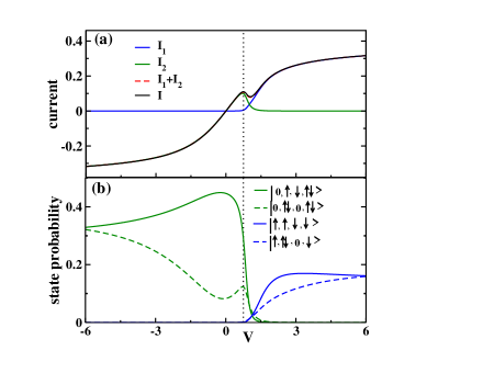
following discussion. Fig 4 shows the results relevant to model (a) with
. In this case, as noticed before,
. Two main contributions to can be recognized as
and
. Quite
interestingly,
as shown in Fig. 4, the sum of these two contributions quantitatively
matches with the
total characteristic.
The states involved in and in only differ by the
occupation at 1st and 4th sites: the states involved in show
single occupancy of sites 1 and 4, while the states involved in
have zero occupation at site 1 and double occupation at site 4.
The position and height of the NDC peak of exactly matches with
the NDC peak of the characteristics: the fall of and the rise of at 0.75
causes the NDC feature in characteristics.
For 0.75, starts decreasing to zero, while increases
to meet at =1.04 resulting a valley in .
So, for 1.04, dominates over resulting in
further increase of total .

The bottom panel of Fig. 4 shows the
weight of the states that mainly contribute to the
current, as shown in the figure label.
The probability of states contributing to (blue lines)
vanishes for : =0 in that region. instead
contributes significantly to total for , where the
contribution from becomes negligible.
The current flows only through the central
bond, and, in a system with and , it
is associated with off-diagonal elements of mixing up states where
both electrons reside on site 2 or are equally distributed in sites 2 and 3. NDC is
observed when the occupancy of the auxiliary sites changes:
the NDC feature occurs when the population of states
contributing to , characterized by ,
start decreasing at the expense of the increasing population of states
contributing to , characterized by .
Model b is more complex, as shown in Fig. 5, collecting the results obtained for and . In this case a variable number of electrons is found in the junction, as shown by the blue lines in Fig. 5a. The characteristic (black line) shows NDC features both in the negative and positive regions, with a more prominent feature at . In the region of interest for NDC the current is mainly due to three specific contribution, as shown in Fig. 5 b. The three contributions are: , and . The states involved in have two electrons in the junction, , while the states contributing to and have . As expected, and contributions become sizable for large negative and positive , respectively. However it is clear from the figure that the NDC features observed in the characteristic are only due to the NDC features observed in the contribution to the total current. For a better understanding, Fig. 5c shows the probability of states playing a main role in transport. drops at the NDC features because the relevant states, having two electrons in the junction, loose their weight and the increasing contributions of either in the negative region or of in the positive region, related to states with , are not able to fully compensate for the loss.
IV conclusions
The current constrained approach offers an alternative picture of transport in nanojunctions with respect to the widespread voltage-constrained approaches. In the CC approach Lagrange multipliers are used to force the system into a current carrying state, then avoiding any explicit reference to semi-infinite electronic reservoirs. The method then applies quite naturally to describe transport in systems with strongly correlated electrons. However, the total number of electrons taking part in transport is fixed in CC approaches, and this has hindered so far the application of the method to problems where charge injection/depletion in the junction is important. This problem could be solved introducing an effective relaxation model that, accounting for the exchange of electrons between the junction and the electrodes, allows the system to relax towards states with different number of electrons. This approach however requires a fairly complex model for relaxation dynamics. Here we borrow from the field of optical spectroscopy a simple phenomenological model for relaxation that maintains constant the number of electrons, and overcome the limitation of fixed number of electrons connecting one or more auxiliary sites to the main junction: while the current does not flow through the auxiliary sites, they exchange electrons with the junction, allowing for a variable number of electrons taking part in transport.
Along these lines we attacked the problem of NDC in a very simple model with a two-site junction connected to two auxiliary sites. NDC is a highly non linear phenomenon: the bistable behavior of the curve at NDC can only be observed in largely cooperative systems. We introduced cooperativity imposing a dependence of the on-site energies of the auxiliary sites on the voltage drop: since the voltage required to support the current depends in turn on the energy of the auxiliary sites, the problem becomes self-consistent and the model supports NDC. Quite interestingly, dangling bonds (side groups) connected to the main current-carrying unit have recently been discussed as responsible for non-linearity in the characteristic curves. Particularly side groups may be responsible for quantum interference phenomena that drastically suppress current.ultimi Our study suggests that a proper choice of the chemical nature of the side groups can not only reduce the current, but eventually lead to NDC.
Here we just investigated an asymmetric junction with weak bonds and a grand-total of four electrons, in two different cases. In the first case we choose equal and opposite on-site energies for the two auxiliary sites leading to a constant number of electrons in the junction (). Minor NDC features are observed in this case, mainly related to an abrupt variation of the occupation of the auxiliary sites. More prominent NDC features are observed in the second model, where, having fixed the energies of the auxiliary sites to the same value, the number of electrons involved in the transport is variable. NDC is related in this case to an abrupt variation with the applied potential of the number of electrons in the junction. In all cases, large and small are needed to observe NDC: weak bonds and large correlations in fact ensure the abrupt variation in the nature of the current carrying state , as required for to observe NDC.
V Acknowledgments
PP acknowledges the CSIR for a research fellowship, SKP acknowledges research support from CSIR and DST, Government of India and AP acknowledges support from the Italian Ministry of Foreign Affairs and Parma University.
References
- (1) A. Nitzan and M. A. Ratner, Science 300, 1384 (2003); W. A. Svec, M. A. Ratner, and M. R. Wasielewsk, Nature 396, 60 (1998); R. G. Endres, D. L. Cox, and R. R. P. Singh, Rev. Mod. Phys. 76, 195 (2004); S. S. Mallajosyula, P. Parida, and S. K. Pati, J. Mat. Chem. 19, 1761 (2009).
- (2) T. Rueckes, K. Kim, E. Joselevich, A. R. Rocha, V. M. Garcasurez, S. W. Bailey, C. J. Lambert, J. Ferrer, and S. Sanvito, Nature Materials 4, 335 (2005); A. Zutic, J. Fabian, and S. D. Sarma, Rev. Mod. Phys., 76, 323 (2004); P. Parida, A. Kundu, and S. K. Pati, Phys. Chem. Chem. Phys. DOI: 10.1039/c004653c (2010); S. K. Pati, J. Chem. Phys. 118, 6529 (2003).
- (3) L. Esaki, Phys. Rev. 109, 603 (1958).
- (4) J. Chen, M. A. Reed, A. M. Rawlett, and J. M. Tour, Science 286, 1550 (2001); J. Chen, W. Wang, M. A. Reed, A. M. Rawlett, D. W. Price, and J. M. Tour, Appl. Phys. Lett. 77, 1224 (2000).
- (5) Z. J. Donhauser, B. A. Mantooth, K. F. Kelly, L. A. Bumm, J. D. Monnell, J. J. Stapleton, D. W. Price, Jr, A. M Rawlett, D. L. Allara, J. M. Tour, and P. S. Weiss, Science 292, 2303 (2001).
- (6) J. M. Seminario, A. G. Zacarias, and J. M. Tour, J. Am. Chem. Soc. 122, 3015 (2000); J. M. Seminario, A. G. Zacarias, and P. A. Derosaet, J. Chem. Phys. 116, 1671 (2002).
- (7) J. Cornil, Y. Karzazi, and J. L. Bredas, J. Am. Chem. Soc. 124, 3516 (2002); S. Lakshmi and S. K. Pati, J. Chem. Phys. 121, 11998 (2004).
- (8) R. Pati and S. P. Karna, Phys. Rev. B 69, 155419 (2004).
- (9) S. Lakshmi and S. K. Pati, Phys. Rev. B 72, 193410 (2005).
- (10) S. Lakshmi, S. Dutta, and S. K. Pati, J. Phys. Chem. C 112, 14718 (2008).
- (11) R. Gutierrez, G. Fagas, G. Cuniberti, F. Grossmann, R. Schmidt, and K. Richter, Phys. Rev. B 65, 113410 (2002).
- (12) R. Pati, M. McClain, and A. Bandyopadhyay, Phys. Rev. Lett. 100, 246801 (2008).
- (13) K. Ono, D. G. Austing, Y. Tokura, and S. Tarucha, Science 297, 1313 (2002).
- (14) K. Ono and S. Tarucha, Phys. Rev. Lett. 92, 256803 (2004).
- (15) A. Thielmann, M. H. Hettler, J. Konig, and G. Schon, Phys. Rev. B 71, 045341 (2005).
- (16) M. H. Hettler, W. Wenzel, M. R. Wegewijs, and H. Schoeller, Phys. Rev. Lett. 90, 076805 (2003).
- (17) M. R. Wegewis, M. H. Hettler, W. Wenzel, and H. Schoeller, Physica E, 18, 241 (2003).
- (18) N. V. Hung, N. V. Lien, and P. Dollfus, Appl. Phys. Lett. 87, 123107 (2005).
- (19) B. Song, D. A. Ryndyk, and G. Cuniberti, Phys. Rev. B 76, 045408 (2007).
- (20) J. Aghassi, A. Thielmann, M. H. Hettler, and G. Schön, Phys. Rev. B 73, 195323 (2006).
- (21) M. Paulsson and S. Stafstrom, Phys. Rev. B 64, 035416 (2001).
- (22) B. Muralidharan and S. Datta, Phys. Rev. B 76, 035432 (2007).
- (23) B. Muralidharan, A. W. Ghosh, and S. Datta, Phys. Rev. B 73, 155410 (2006).
- (24) S. Datta, Nanotechnology 15, S433 (2004).
- (25) B. Muralidharan, A. W. Ghosh, S. K. Pati, and S. Datta, IEEE Transac. on Nanotech. 6, 536 (2007).
- (26) P. Parida, S. Lakshmi, and S. K Pati, J. Phys.: Cond. Matt. 21, 095301 (2009).
- (27) A. Kamenev and W. Kohn, Phys. Rev. B 63, 155304 (2001).
- (28) P. Bokes, H. Mera, and R. W. Godby, Phys. Rev. B 72, 165425 (2005).
- (29) F. Green, J. S. Thakur,and M. P. Das, Phys. Rev. Lett 92, 156804 (2004); M. P. Das and F. Green, J. Phys. Cond. Matt. 15, L687 (2003).
- (30) T. K. Ng, Phys. Rev. Lett. 68, 1018 (1992).
- (31) W. Magnus and W. Schoenmaker, Phys. Rev. B 61, 10883 (2000).
- (32) D. S. Kosov, J. Chem. Phys. 116, 6368 (2002).
- (33) D. S. Kosov, J. Chem. Phys. 120, 7165 (2004).
- (34) K. Burke, R. Car, and R. Gebauer, Phys. Rev. Lett. 94, 146803 (2005).
- (35) A. Painelli, Phys. Rev. B 74, 155305 (2006).
- (36) W. Kohn, Phys. Rev. 133, A171 (1964).
- (37) P. F. Maldague, Phys. Rev. B bf 16, 2437 (1977).
- (38) M. Esposito, U. Harbola, S. Mukamel, Rev. Mod. Phys. 81, 1665 (2009).
- (39) S. Mukamel, Principles of Nonlinear Optical Spectroscopy (Oxford University Press, New York, 1995).
- (40) R. W. Boyd, Nonlinear Optics (Academic Press, New York, 2003).
- (41) R. R. Chance, A. Prock, and R. Silbey, Adv. Chem. Phys. 37, 1 (1978); M. Galperin and A. Nitzan, Phys. Rev. Lett. 95, 206802 (2005).
- (42) G.C. Solomon, D. Q. Andrews, R. H. Goldsmith, T. Hansen, M. R. Wasielewski, R. P. Van Duyne, M. A. Ratner, J. Am. Chem. Soc. 130, 17301 (2008); G. C. Solomon, D.Q. Andrews, R. P. Van Duyne, M. A. Ratner, ChemPhysChem 10, 257 (2009).