Quantized Charge Pumping through a Carbon Nanotube Double Quantum Dot
Abstract
We demonstrate single-electron pumping in a gate-defined carbon nanotube double quantum dot. By periodic modulation of the potentials of the two quantum dots we move the system around charge triple points and transport exactly one electron or hole per cycle. We investigate the pumping as a function of the modulation frequency and amplitude and observe good current quantization up to frequencies of 18 MHz where rectification effects cause the mechanism to break down.
pacs:
73.63.Fg, 73.63.Kv, 73.23.HkFast and accurate control of the charge state of quantum dots is important in research areas varying from quantum information processing to quantum metrology. Quantum computation schemes based on charge or spin qubits defined in quantum dots Loss , for example, require manipulation of the charge state well within the coherence times of the qubits which, in practise, implies nanosecond control. In quantum metrology, efforts towards the development of a current standard require the transfer of single electrons at nanosecond timescales with a precision of 0.1 part per million or better Zimmerman . The ability of fast control of the charge states of carbon nanotube quantum dots is of particular interest in these respects. In quantum information processing, carbon nanotube quantum dots are attractive as electron spin coherence times are expected to be long and because spin-orbit interaction Kuemmeth ; Jespersen ; Chorley1 allows for electrical or even optical Galland control of the spin states. Carbon nanotube quantum dots are also promising as single electron pumps in quantum metrology for use in a current standard. The ultimate precision of single-electron pumps is widely regarded to be dependent on the strength of electron-electron interactions, suppressing errors due to co-tunneling events Jensen . These interactions are exceptionally strong in carbon nanotubes. In addition, when combined with electron-hole recombination, the ability to transfer single electrons in semiconducting nanotubes at well defined intervals has potential in quantum optics as an electrically-driven on-demand single-photon source in the infrared frequency range Mueller ; Hogele .
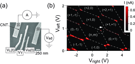
Here we demonstrate single-electron pumping in a gate-defined carbon nanotube double quantum dot by periodic modulation of the potentials of the two quantum dots around charge triple points in the stability diagram. We investigate the pumping as a function of the modulation frequency and amplitude and show quantized charge pumping up to frequencies of 18 MHz, corresponding to a period of nanoseconds. The device we consider is a single-walled carbon nanotube grown by chemical vapour deposition on degenerately doped Si terminated by 300 nm SiO2, see Fig. 1(a). To define a double quantum dot, the nanotube is contacted by evaporated source and drain electrodes of Ti/Au which form the outer tunnel barriers of the quantum dots. A capacitively coupled top gate, separated from the nanotube by nm of AlOx is used to control the tunnel coupling between the dots. The outer two plunger gates, set back from the nanotube, control the electron number on each dot.
The device was bonded onto microwave printed circuit board and mounted on the tail of a mK dilution refrigerator. The two plunger gates are connected to semirigid coaxial cables via bias tees at the mixing chamber, allowing dc and rf signals to be applied. The source is connected to a resonant circuit with dc connection to allow simultaneous transport and rf reflectometry measurements Chorley2 . High frequency synthesized waveforms were applied to the gates using a Tektronix AWG5014 arbitrary waveform generator and the current through the nanotube device is measured by a Keithley 6514 electrometer.
At low temperatures, quantum dots form between each contact and the central barrier. For appropriate settings of the Si back gate voltage V and top gate voltage V, the charge stability diagram displays the characteristic honeycomb pattern of a double quantum dot Wiel ; Graber , see Fig. 1(b). The electron occupation number of the quantum dots is indicated by the ordered pairs . A finite conductance is observed at the triple points where three different charge states are degenerate. Weak co-tunneling is observed for some charge transitions of the left quantum dot but mostly suppressed otherwise. The charging energies of the two quantum dots can be obtained from the charge stability diagrams and yield and meV for the left and right quantum dot, respectively. The interdot charging energy meV.
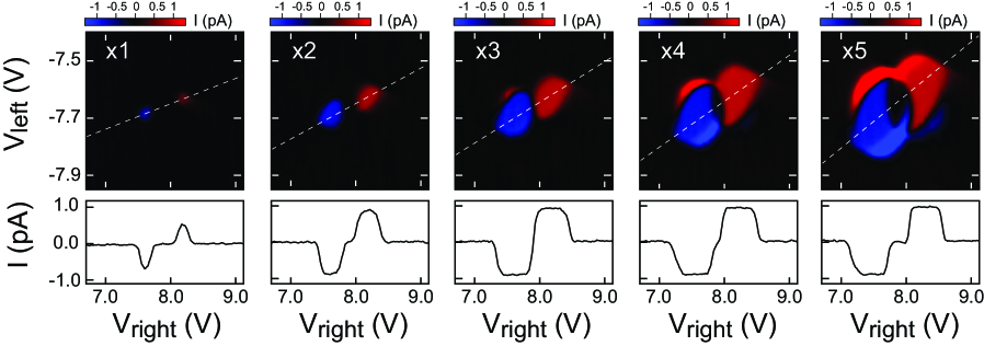
Following a technique first demonstrated for metallic single-electron tunneling devices Pothier , the occupation number of the quantum dots is varied periodically by applying a small sinusoidal voltage to each plunger gate with a 90∘ phase shift between them such that the gates trace out approximately circular paths on the stability diagram amplitude . The centers of the circular paths are then varied by addition of a dc signal offset while the source-drain bias is kept at zero. Figure 2 shows the resulting current around a representative triple point pair of our nanotube double quantum dot for a modulation frequency MHz and a sequence of increasing amplitude. The line traces show the current along the dashed lines in the top panels for each measurement. For the lowest pumping amplitude, current peaks of opposite polarity are observed at the two triple points and the current is zero elsewhere. As the amplitude of the signal is increased, clear current plateaus of about 0.96 pA are observed. The plateaus are flat within our measurement accuracy of fA.
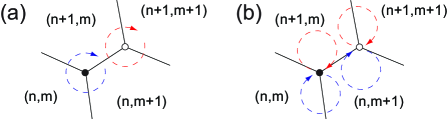
These observations can be understood considering the pumping sequence illustrated in Fig. 3(a). When a path on the stability diagram encircles a triple point, exactly one electron or hole moves between the electrodes per cycle and the current is expected to be quantized as , where is the electron charge Pothier ; Fuhrer . For the leftmost trajectory in Fig. 3(a), for example, electrons are moved in the sequence . When the same path is encircling the other triple point of a pair, the polarity of the current is reversed. For the modulation frequency MHz used in Fig. 2, this corresponds to the observed currents of 0.96 pA. The area in the stability diagram in which a quantized current is observed increases with pumping amplitude up to a maximum set by . As expected, the magnitude of the current observed on the plateaus in Fig. 2 does not increase with pumping amplitude and depends on the modulation frequency only. With increasing pumping amplitudes (rightmost plots), there are trajectories that include both triple points such that no charge is transferred between the dots but only between the dots and leads, i.e., following a sequence . This results in an area of zero current in between the plateaus.
In the rightmost plots of Fig. 2, another effect becomes visible where non-quantized currents are observed above and below the quantized regions. These positions in the stability diagram correspond to those trajectories that cross the triple points where the double dot has a finite conductance and a non-quantized current flows when . The effect can therefore be understood as rectification where modulation of the source and drain potentials by the plunger gates - to which they are capacitively coupled - induces a current. The polarity of the rectified currents depends on the direction of the trajectories in the stability diagram near the triple points clockwise , as indicated in Fig. 3(b). Rectification effects become stronger for larger amplitudes and frequencies preventing us from observing a clean quantized current above MHz.
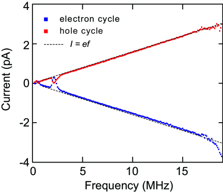
These observations are further illustrated by Fig. 4 which shows the current at the triple points for increasing frequencies. The current follows the expected relation , indicated by the dashed lines, upto 18 MHz where it starts to deviate phase as rectification effects become dominant. We note that 18 MHz is a much smaller frequency than the intrinsic dynamic limit of the device which is given by its time constant Jensen ; Reilly and which we estimate to be of order 1-10 GHz estimate . This suggests that current quantization could be observed for much larger modulation frequencies if rectification can be sufficiently suppressed. Indeed, in previous work in which potential modulation of nanotube quantum dots was achieved by surface-acoustic-waves (SAW) - avoiding direct coupling between the rf source and nanotube contacts - quantized currents in the GHz range were observed Buitelaar ; Wurstle . We believe rectification can be reduced in the present double dot devices by a different choice of substrate, e.g., undoped Si or quartz, and stronger coupling between the quantum dots and plunger gates.
In conclusion, we demonstrate charge pumping in a carbon nanotube double quantum by periodic modulation of the dot potentials. We investigate the pumping as a function of the modulation amplitude and frequency and observe quantized currents up to frequencies of MHz. Above this frequency, rectification prevents us from observing the quantization cleanly. We believe that for an optimized device geometry accurately quantized currents in the GHz range are experimentally feasible.
We thank David Cobden and Jiang Wei for the carbon nanotube growth and Karl Petersson, Victoria Russell, and Mamta Thangaraj for technical assistance. This work was supported by EPSRC, the Newton Trust and the Royal Society (M.R.B.).
References
- (1) D. Loss and D.P. DiVincenzo, Phys. Rev. A 57, 120 (1998).
- (2) N.M. Zimmerman, Physics Today 63, 68 (2010).
- (3) F. Kuemmeth, S. Ilani, D.C. Ralph, and P.L. McEuen, Nature (London) 452, 448 (2008).
- (4) T.S. Jespersen, K. Grove-Rasmussen, J. Paaske, K. Muraki, T. Fujisawa, J. Nygård, and K. Flensberg, Nature Phys. 7, 348 (2011).
- (5) S.J. Chorley, G. Giavaras, J. Wabnig, G.A.C. Jones, C.G. Smith, G.A.D. Briggs, and M.R. Buitelaar, Phys. Rev. Lett. 106, 206801 (2011).
- (6) C. Galland and A. Imamoǧlu, Phys. Rev. Lett. 101, 157404 (2008).
- (7) H.D. Jensen and J.M. Martinis, Phys. Rev. B 46, 13407 (1992).
- (8) T. Mueller, M. Kinoshita, M. Steiner, V. Perebeinos, A.A. Bol, D.B. Farmer, and P. Avouris, Nature Nanotech. 5, 27 (2010).
- (9) A. Hogele, C. Galland, M. Winger, A. Imamoglu, Phys. Rev. Lett. 100, 217401 (2008).
- (10) S.J. Chorley, J. Wabnig, Z.V. Penfold-Fitch, K.D. Petterson, J. Frake, C.G. Smith, and M.R. Buitelaar, Phys. Rev. Lett. 108, 036802 (2012).
- (11) W.G. van der Wiel, S. De Franceschi, J.M. Elzerman, T. Fujisawa, S. Tarucha, and L.P. Kouwenhoven, Rev. Mod. Phys. 75, 1 (2002).
- (12) M.R. Gräber, W.A. Coish, C. Hoffmann, M. Weiss, J. Furer, S. Oberholzer, D. Loss, and C. Schönenberger, Phys. Rev. B 74, 075427 (2006).
- (13) H. Pothier, P. Lafarge, C. Urbina, D. Esteve, and M.H. Devoret, Europhys. Lett. 17, 249 (1992).
- (14) The amplitude of the two output signals at the waveform generator is tuned such that the potential modulation at the device is of similar strength for both dots. Since the right gate is more weakly coupled to the right dot as compared to the coupling between the left plunger gate and left dot by a factor , the voltage we applied to the right plunger is correspondingly larger.
- (15) A. Fuhrer, C. Fasth, and L. Samuelson, Appl. Phys. Lett. 91, 052109 (2007).
- (16) We verified that both the quantized and non-quantized currents reverse polarity as the direction of the trajectories is changed from clockwise to anti-clockwise.
- (17) At MHz, a resonance in one of the plunger gate’s transmission lines changes the phase angle and power of the signal, resulting in a change of the polarity of the pumped current.
- (18) D.J. Reilly and T.M. Buehler, Appl. Phys. Lett. 87, 163122 (2005).
- (19) Here we use a resistance M and capacitance aF as deduced from the dc transport measurements.
- (20) M.R. Buitelaar, P.J. Leek, V.I. Talyanskii, C.G. Smith, D. Anderson, G.A.C. Jones, J. Wei, and D.H. Cobden, Semicond. Sci. Technol. 21, S69 (2006).
- (21) C. Würstle, J. Ebbecke, M.E. Regle, and A. Wixforth, New Journal of Physics 9, 73 (2007).