Designing all-graphene nanojunctions by covalent functionalization
Abstract
We investigated theoretically the effect of covalent edge functionalization, with organic functional groups, on the electronic properties of graphene nanostructures and nano-junctions. Our analysis shows that functionalization can be designed to tune electron affinities and ionization potentials of graphene flakes, and to control the energy alignment of frontier orbitals in nanometer-wide graphene junctions. The stability of the proposed mechanism is discussed with respect to the functional groups, their number as well as the width of graphene nanostructures. The results of our work indicate that different level alignments can be obtained and engineered in order to realize stable all-graphene nanodevices.
Dipartimento di Fisica, Università di Modena e Reggio Emilia, I-41125 Modena, Italy \alsoaffiliationDipartimento di Fisica, Università di Modena e Reggio Emilia, I-41125 Modena, Italy \alsoaffiliationDipartimento di Fisica, Università di Modena e Reggio Emilia, I-41125 Modena, Italy
TOC Graphic
![[Uncaptioned image]](/html/1203.6568/assets/toc.png)
Keywords: semi-empirical methods, carbon nanostructures, frontier orbitals line up, organic moieties
The successful fabrication of the two-dimensional system graphene 1 and its excellent mechanical and electronic properties have aroused great interest in several different fields, both from fundamental research and for technological applications 2, 3, 4, 5. Quasi-one-dimensional graphene nanoribbons (GNRs) with semiconducting behavior can also be obtained, 6, 7 with electrical band gap tunable within a wide range, 8, 9 and their optical properties, even if less intensively studied, offer stimulating perspectives 10, 11, 12, 13. One main challenge is to gain control of the graphene edge morphology at the nanoscale, in view of designing all-graphene nano-devices. In this sense many recent improvements in production techniques were reported, including both top-down 14, 15, 16, 17, 18, 19, 20, 21 and bottom-up 22, 23 approaches, which point to the possibility of exploiting the exceptional properties of graphene nanostructures in actual devices (see e.g. Refs. 24, 25, 26).
In view of electronic and optoelectronic applications, it is important to identify further approaches for an efficient engineering of the electronic states of a graphene nanostructure. It has recently been shown that the electronic properties of graphene-based systems can be conveniently modulated by means of organic functionalization 27, 28, 29, 30. Until now, a number of procedures have been proposed exploiting either surface functionalization through chemisorption of molecules 31, 32, 33, which is expected however to damage the transport properties of the system, or non-covalent interaction 34, 35, 36, 37, which usually induces doping effects but does not lead to stable structures. A more effective strategy could be edge functionalization 38, 39, which may offer promising perspectives also in so far unexplored application fields, such as the production of GNR-based nanojunctions.
In semiconductor physics, heterojunctions are usually classified on the basis of the relative alignment of valence and conduction band states at the interface of the two materials. Heterostructures where the band gap of one semiconductor is fully contained in the gap of the other are commonly indicated as type I or straddling. On the other hand, the so called type II or staggered alignment is achieved when the top of valence band and the bottom of conduction band of one semiconductor are both higher in energy compared to the corresponding states of the other, so that the top of the valence band of the junction lies on one side of the interface, and the bottom of conduction on the other side. In this case, electrons and holes on the frontier orbitals are spatially separated, being located on opposite sides of the junction, which may promote relevant processes, such as e.g. photoinduced charge separation, as requested by light harvesting applications, or photocatalysis. These concepts can be extended to graphene nanojunctions, where the seamless covalent transition from two graphene nanostructures with different electronic characteristics can create, as in conventional semiconductor heterojunctions, different kind of alignments. Indeed, interfacing semiconducting GNRs with different widths, and consequently different energy gaps, provides a type I level line-up12, 40. In this paper we propose a proof of concept for a viable method to realize all-graphene type II nanojunctions. For this purpose we investigate the effects of stable edge functionalization through organic electron-donating and electron-withdrawing groups, which modify electron affinities and ionization potentials in comparison with the H-terminated GNR. The proposed model for chemical engineering carries a high potential for producing stable graphene nanostructures, preserving their flexibility and their intrinsic electronic features, carbon network being unaltered upon functionalization.
1 Methods
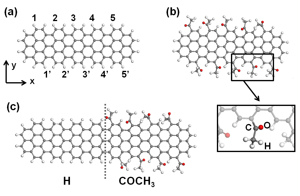
As prototypes for graphene nanoribbons we consider sub-nanometer-wide graphene nanoflakes (GNFs), that is, finite systems, and we focus in particular on H-terminated GNFs [1(a)], organically functionalized GNFs [1(b)], as well as on the nanojunction obtained by functionalizing one half of the flake with -\ceCOCH3 groups [1(c)]. In this case, we will be interested in the frontier molecular orbitals (that stand here for the conduction and valence band states) and their localization and energy alignment across the differently terminated regions. In order to have access to the electronic energies, we performed calculations in the frame of the semi-empirical AM1 scheme 41, 42. AM1 is a well tested method based on the Hartree-Fock scheme 43, suitable for finite structures; 44, 45, 46, 47, 48, 49, 50 it allows one to evaluate the ground state properties of the system and to compute the electrical band gap as the difference between electron affinity (EA) and ionization potential (IP). The latter quantities are expressed in terms of the total energy of the neutral [E(0)] and charged systems [E(1)], in the usual way EA = E(0) - E(-1) and IP = E(+1) - E(0). For all the considered structures, we performed full geometrical optimization to evaluate E(0), with a threshold for the forces of 0.4 /Å. The E(1) are obtained at the fixed atomic positions optimized in the ground state, i.e. vertical EA and IP are computed.
2 Results and Discussion
Our reference system is the \ceC80H28 flake [1(a)], characterized by armchair-shaped H-saturated edges along the length (x direction in 1). We checked that the chosen length/width ratio is such that the zigzag-shaped end-borders (y direction) do not affect the intrinsic properties related to the armchair edges along the length. Thus, \ceC80H28 is a suitable model for an armchair GNR of width parameter N=7, N being the number of dimer lines across the ribbon width, according to the standard notation 8. It corresponds to an effective width of 7 Å, defined as the distance between C atoms on opposite edges, belonging to the same zigzag chain along . Next, we addressed the same GNF upon covalent edge functionalization with organic groups. We started focusing on molecules containing a ketone functional group, characterized by high electronegativity of its carbonyl oxygen atoms, and in particular we considered the methyl ketone group -\ceCOCH3 [inset in 1(b)], which is known to be more stable than the simpler formaldehyde group -COH. We simulated full functionalization of the \ceC80H28 by replacing each second H atom along the length with methyl ketone, corresponding in this case to ten anchored groups per flake [\ceC80H18\ce(COCH3)10], i.e. five per edge side, as shown in 1(b). We computed , EA and IP, and we compared these quantities to those evaluated for \ceC80H28 by calculating EA (IP) as the difference between EA (IP) of the functionalized and hydrogenated GNF, respectively. A positive shift of both EA and IP is revealed, as shown in the second column of 1.
![[Uncaptioned image]](/html/1203.6568/assets/H2.png) |
![[Uncaptioned image]](/html/1203.6568/assets/acet2.png) |
![[Uncaptioned image]](/html/1203.6568/assets/difluoroethene2.png) |
![[Uncaptioned image]](/html/1203.6568/assets/trifluoroethenol2.png) |
![[Uncaptioned image]](/html/1203.6568/assets/methanol2.png) |
![[Uncaptioned image]](/html/1203.6568/assets/ethene2.png) |
![[Uncaptioned image]](/html/1203.6568/assets/buthene2.png) |
|
| H | -\ceCOCH3 | -\ceCH=CF2 | -\ceOCF=CF2 | -\ceOCH3 | -\ceCH=CH2 | -\ce(CH)3=CH2 | |
| [eV] | 5.13 | 4.86 | 4.65 | 4.74 | 4.75 | 4.76 | 4.67 |
| EA [eV] | 0.00 | 0.69 | 0.67 | 0.70 | -0.12 | 0.14 | 0.15 |
| IP [eV] | 0.00 | 0.42 | 0.19 | 0.31 | -0.50 | -0.22 | -0.31 |
In addition to the methyl ketone group, we considered the case of other organic functionalizations. We focused on few prototypical substituents, such as (i) a methoxy group (-\ceOCH3), characterized by an O-bridge ester bond, which is known to be electron-donating with respect to aromatic molecules 51; (ii) a -\ceCH=CF2 group, which is expected to be electron-withdrawing, due to the high electronegativity of its F-termination; (iii) a -\ceOCF=CF2 group, which combines the presence of O-bridge ester bond and halogen termination. Due to their characteristics, we expect group (i) to provide a similar effect compared to methyl ketone, i.e. to rise EA and IP with respect to the hydrogenated flake, and group (ii) to do the opposite. In the case of -\ceOCF=CF2 the coexistence of both O-bridge bond and F-termination makes the picture less predictable. We also consider -\ceCH=CH2 and -\ce(CH)3=CH2 functionalizations which do not introduce any foreign species in the system and preserve its C- conjugation through the alternation of single and double C-C bonds. For each chosen group we addressed full functionalization, analogously to the case of -\ceCOCH3 illustrated in 1(b), and we computed , EA and IP.
By inspecting the complete results in 1, two main features arise. The first is related to a decrease of the energy gap, independently of the anchored group: this is ascribed to an increase of the effective width of the flake, compared to the fully hydrogenated case. The other important outcome concerns the sign of EA and IP: we observe positive (negative) values of both EA and IP, corresponding to a downshift (upshift) of both HOMO and LUMO for groups with a predominant electron-withdrawing (-donating) character, as well as for -\ceOCF=CF2. On the contrary, -\ceCH=CH2 and -\ce(CH)3=CH2 functionalizations produce EA and IP having opposite signs: given the simple bond-alternating character of the functional group, the major result is related to the extension of the wave function to a larger effective width, which thus reduces in agreement with results for one-dimensional GNRs 12.
The analysis of Mulliken charge population shows that a charge redistribution at the edge occurs upon functionalization. In particular Mulliken charges of functionalized C edge atoms become more positive, being these atoms bonded to more electronegative species than H. Larger differences (¿ 0.2 ) are observed when functional groups are bonded to the flake through an O-bridge ester bond, i.e. -\ceOCH3 and -\ceOCF=CF2. On the other hand, moieties bonded through C atoms induce slighter Mulliken charge redistribution, of the order or less than 0.1 . It is important to highlight that these redistribution effects vanish within one aromatic ring.
| H | 2 | 4 | 6 | 8 | 10 | |
|---|---|---|---|---|---|---|
| [eV] | 5.13 | 5.01 | 5.01 | 4.99 | 4.96 | 4.86 |
| EA [eV] | 0.00 | 0.21 | 0.29 | 0.37 | 0.47 | 0.69 |
| IP [eV] | 0.00 | 0.09 | 0.17 | 0.23 | 0.30 | 0.42 |
We also performed some tests on functionalized \ceC80H28 at decreasing number of functional groups (see 2). We focus here in -\ceCOCH3 as an illustrative example but this behavior is independent of the anchored group. We take the hydrogenated flake and, retaining the symmetry of the system, we introduce increasing even numbers of functional groups, up to ten, which corresponds to full functionalization for the chosen \ceC80H28 flake (see 1(b)). We start from two anchored groups in positions 3 and 3’, after the scheme in 1(a), which corresponds to a -\ceCOCH3 substituent each fifth H atom. We then introduce four and six groups in positions (2, 2’, 4, 4’) and (1, 1’, 3, 3’, 5, 5’) respectively. In the case of eight bonded groups, in order to maintain the symmetry of the graphene flake, each H atom in positions (1, 1’, 2, 2’, 4, 4’, 5, 5) is replaced by a -\ceCOCH3. The results, reported in 2, show a monotonic growth of both EA and IP with increasing number of covalently bonded groups, with an almost linear dependence for IP. At the same time, we notice the monotonic decrease of , consistently with the above mentioned picture related to the increased effective width of the GNF.
We also discuss the dependence of the electronic properties of the GNF, specifically related to EA and IP, by directly increasing its width. For this purpose, we performed a systematic investigation on GNFs, characterized by fixed length (along direction in 1) and increasing width (along direction), fully functionalized with 16 -\ceCOCH3 groups 52. We studied eight GNFs ranging from width parameter N=4 (less than 4 Å wide) to N=11 (about 12 Å wide) and we computed EA and IP for each of them.
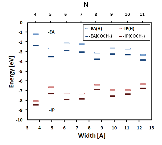
As shown in 2, the calculated values for EA and IP have an oscillating behavior characterized by the modulo 3 periodicity already encountered in infinite GNRs 53, 54, 8, with the smallest value of the energy gap pertaining to the N= family ( integer). An approximate dependence (being the GNF width) is recognizable for the energy gap, consistently with well known theoretical 8, 9 and experimental 6, 7 results. The values of EA and IP, represented in 2 by the spacing between the respective marks, show a faster decay, which may be compatible with a local dipole mechanism driving the offset between functionalized and hydrogenated flakes. For instance, for the family, we get values of EA=0.85 eV and IP=0.67 eV for the smallest computed flake (N=5, =4.9 Å) and EA=0.53 eV and IP=0.43 eV for the largest one (N=11, =12.3 Å). From the results in 2, we can extrapolate non negligible effects of covalent functionalization also for nanometer-sized graphene flakes, which can be considered realistic for current nanofabrication approaches.
Finally, we directly investigate the type II nanojunction obtained by connecting a fully hydrogenated GNF to a fully functionalized one, having the same width (see 1(c)). For this purpose we adopted a flake of the same width of \ceC80H28 but increased global length, in order to ensure that each side of the junction is long enough to confidently reproduce the bulk properties of the flake (i.e. same single-particle orbitals in the energy range close to the energy gap). The resulting system accommodates full functionalization of one half flake with eight radicals, four per side (see 1(c)).
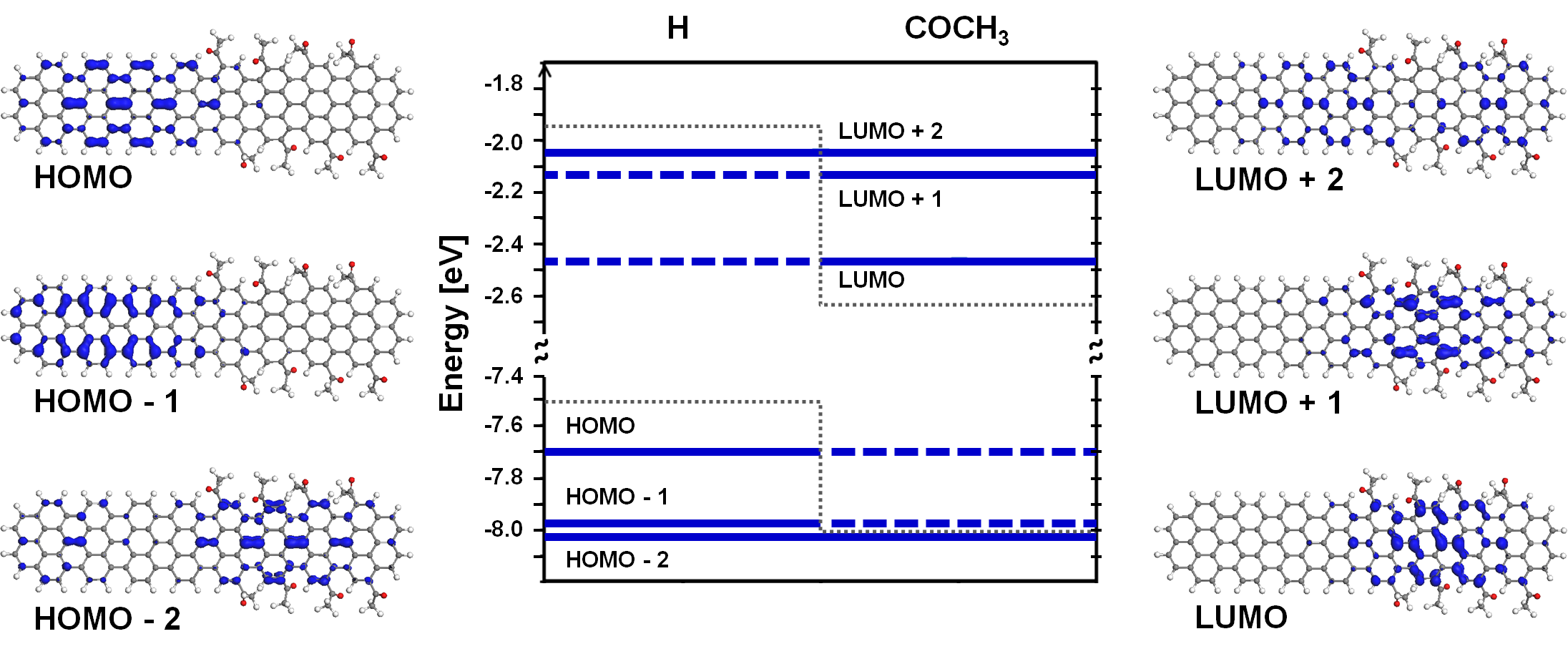
We first performed full geometrical optimization and then focused on the ground state electronic properties of the junction. In particular we are interested in the energy and wave function localization of the frontier states, as summarized in 3. The analysis of the wave function distributions clearly reflects the type II character of this junction. In fact we observe that the top valence states, HOMO and HOMO-1, are localized on the hydrogenated side of the junction, while the bottom conduction states, LUMO and LUMO+1, are localized on the functionalized side. On the other hand the next states HOMO-2 and LUMO+2 show already resonant character. This feature can be explained in terms of the absolute energy levels of the bulk of the two sides, as indicated in the graph of 3: we represent by the dotted grey line the gap of the homogeneous systems, hydrogenated and functionalized, evaluated from the HOMO and LUMO levels of the fully hydrogenated [\ceC116H40] and functionalized [\ceC116H24\ce(COCH3)16] GNFs. On top of this we plot the level spectrum for the junction-GNF, highlighting the localization character of the related state through blue solid (finite probability) or dashed (zero probability) lines. We see that HOMO and HOMO-1 lie in the forbidden gap for the functionalized side and are consistently localized on the allowed hydrogenated half; the opposite applies to LUMO and LUMO+1, which are thus localized on the functionalized part. While the numbers for IP and EA in 2 are taken from total energy calculations, therefore giving us good precision, we remark that the energy level spectrum shown here is by construction based on one-electron mean-field approximation and cannot give us a level-by-level accuracy, in particular for the unoccupied states. We see however that the overall picture is totally consistent with the type II alignment.
3 Conclusions
In conclusion, we have studied the effects of organic covalent functionalization on sub-nanometer sized graphene nanoflakes, by varying the anchored groups, the number of functionalizing groups and the flake width. Our results indicate that edge functionalization can be designed to tune the electronic properties of graphene nanostructures and to control band alignment in graphene nano-junctions, while preserving stability and intrinsic electronic properties. This opens the possibility to realize stable all-graphene electronic and optoelectronic nanodevices based on type II offset 55.
The authors acknowledge CINECA for computational support and Stefano Corni and Enrico Benassi for helpful discussions. This work was partly supported by “Fondazione Cassa di Risparmio di Modena”, by the Italian Ministry of Foreign Affairs (Italy-USA bilateral project) and by the Italian Ministry of University and Research under FIRB grant ItalNanoNet. MJC acknowledges support from FAPESP and CNPq (Brazil).
References
- Novoselov et al. 2004 Novoselov, K. S.; Geim, A. K.; Morozov, S. V.; Jiang, D.; Zhang, Y.; Dubonos, S. V.; Grigorieva, I. V.; Firsov, A. A. Electric Field Effect in Atomically Thin Carbon Films. Science 2004, 306, 666–669
- Soldano et al. 2010 Soldano, C.; Mahmood, A.; Dujardin, E. Production, properties and potential of graphene. Carbon 2010, 48, 2127–2150
- Geim 2009 Geim, A. Graphene: status and prospects. Science 2009, 324, 1530
- Burghard et al. 2009 Burghard, M.; Klauk, H.; Kern, K. Carbon-Based Field-Effect Transistors for Nanoelectronics. Adv. Mater. 2009, 21, 2586–2600
- Castro Neto et al. 2009 Castro Neto, A. H.; Guinea, F.; Peres, N. M. R.; Novoselov, K. S.; Geim, A. K. The electronic properties of graphene. Rev. Mod. Phys. 2009, 81, 109–162
- Han et al. 2007 Han, M. Y.; Ozyilmaz, B.; Zhang, Y.; Kim, P. Energy Band-Gap Engineering of Graphene Nanoribbons. Phys. Rev. Lett. 2007, 98, 206805
- Chen et al. 2007 Chen, Z.; Lin, Y.-M.; Rooks, M. J.; Avouris, P. Graphene nano-ribbon electronics. Physica E 2007, 40, 228 – 232
- Son et al. 2006 Son, Y.-W.; Cohen, M. L.; Louie, S. G. Energy Gaps in Graphene Nanoribbons. Phys. Rev. Lett. 2006, 97, 216803
- Yang et al. 2007 Yang, L.; Park, C.-H.; Son, Y.-W.; Cohen, M. L.; Louie, S. G. Quasiparticle Energies and Band Gaps in Graphene Nanoribbons. Phys. Rev. Lett. 2007, 99, 186801
- Prezzi et al. 2008 Prezzi, D.; Varsano, D.; Ruini, A.; Marini, A.; Molinari, E. Optical properties of graphene nanoribbons: The role of many-body effects. Phys. Rev. B 2008, 77, 041404(R)
- Prezzi et al. 2007 Prezzi, D.; Varsano, D.; Ruini, A.; Marini, A.; Molinari, E. Optical properties of one-dimensional graphene polymers: the case of polyphenanthrene. Phys. Status Solidi B 2007, 244, 4124–4128
- 12 Prezzi, D.; Varsano, D.; Ruini, A.; Molinari, E. submitted 2010.
- Yang et al. 2007 Yang, L.; Cohen, M.; Louie, S. Excitonic Effects in the Optical Spectra of Graphene Nanoribbons. Nano Lett. 2007, 7, 3112–3115
- Datta et al. 2008 Datta, S. S.; Strachan, D. R.; Khamis, S. M.; Johnson, A. T. C. Crystallographic Etching of Few-Layer Graphene. Nano Lett. 2008, 8, 1530–6984
- Campos et al. 2009 Campos, L. C.; Manfrinato, V. R.; Sanchez-Yamagishi, J. D.; Kong, J.; Jarillo-Herrero, P. Anisotropic Etching and Nanoribbon Formation in Single-Layer Graphene. Nano Lett. 2009, 9, 1530–6984
- Li et al. 2008 Li, X.; Wang, X.; Zhang, L.; Lee, S.; Dai, H. Chemically Derived, Ultrasmooth Graphene Nanoribbon Semiconductors. Science 2008, 319, 1229–1232
- Wang and Dai 2010 Wang, X.; Dai, H. Etching and narrowing of graphene from the edges. Nature Chem. 2010, 2, 661–665
- Jia et al. 2009 Jia, X.; Hofmann, M.; Meunier, V.; Sumpter, B.; Campos-Delgado, J.; Romo-Herrera, J.; Son, H.; Hsieh, Y.-P.; Reina, A.; Kong, J.; Terrones, M.; Dresselhaus, M. Controlled Formation of Sharp Zigzag and Armchair Edges in Graphitic Nanoribbons. Science 2009, 323, 1701
- Kosynkin et al. 2009 Kosynkin, D. V.; Higginbotham, A. L.; Sinitskii, A.; Lomeda, J. R.; Dimiev, A.; Price, B. K.; Tour, J. M. Longitudinal unzipping of carbon nanotubes to form graphene nanoribbons. Nature (London) 2009, 458, 872
- Jiao et al. 2009 Jiao, L.; Zhang, L.; Wang, X.; Diankov, G.; Dai, H. Narrow graphene nanoribbons from carbon nanotubes. Nature (London) 2009, 458, 877
- Cano-Márquez et al. 2009 Cano-Márquez, A. G.; Rodríguez-Macías, F. J.; Campos-Delgado, J.; Espinosa-González, C. G.; Tristán-López, F.; Ramírez-González, D.; Cullen, D. A.; Smith, D. J.; Terrones, M.; ; Vega-Cantú, Y. I. Ex-MWNTs: Graphene Sheets and Ribbons Produced by Lithium Intercalation and Exfoliation of Carbon Nanotubes. Nano Lett. 2009, 9, 1527
- Yang et al. 2008 Yang, X.; Dou, X.; Rouhanipour, A.; Zhi, L.; Rader, H. J.; Muellen, K. Two-Dimensional Graphene Nanoribbons. J. Am. Chem. Soc. 2008, 130, 4216
- Cai et al. 2010 Cai, J.; Ruffieux, P.; Jaafar, R.; Bieri, M.; Braun, T.; Blankenburg, S.; Muoth, A. P., Matthiasand Seitsonen; Saleh, M.; Feng, X.; Muellen, K.; Fasel, R. Atomically precise bottom-up fabrication of graphene nanoribbons. Nature (London) 2010, 466, 470–473
- Wang et al. 2008 Wang, X.; Ouyang, Y.; Li, X.; Wang, H.; Guo, J.; Dai, H. Room-Temperature All-Semiconducting Sub-10-nm Graphene Nanoribbon Field-Effect Transistors. Phys. Rev. Lett. 2008, 100, 206803
- Xia et al. 2009 Xia, F.; Mueller, T.; Lin, Y.; Valdes-Garcia, A.; Avouris, P. Ultrafast graphene photodetector. Nature Nanotech. 2009, 4, 839–843
- Ponomarenko et al. 2008 Ponomarenko, L.; Schedin, F.; Katsnelson, M.; Yang, R.; Hill, E.; Novoselov, K.; Geim, A. Chaotic Dirac billiard in graphene quantum dots. Science 2008, 320, 356
- Loh et al. 2010 Loh, K.; Bao, Q.; Ang, P.; Yang, J. The chemistry of graphene. J. Mater. Chem. 2010, 20, 2277–2289
- Farmer et al. 2009 Farmer, D. B.; Golizadeh-Mojarad, R.; Perebeinos, V.; Lin, Y.-M.; Tulevski, G. S.; Tsang, J. C.; Avouris, P. Chemical doping and electron-hole conduction asymmetry in graphene devices. Nano Lett. 2009, 9, 388–392
- Farmer et al. 2009 Farmer, D. B.; Lin, Y.-M.; Afzali-Ardakani, A.; Avouris, P. Behavior of a chemically doped graphene junction. Appl. Phys. Lett. 2009, 94, 213106
- Lohmann et al. 2009 Lohmann, T.; von Klitzing, K.; Smet, J. Four-Terminal Magneto-Transport in Graphene pn Junctions Created by Spatially Selective Doping. Nano Lett. 2009, 9, 1973–1979
- Lopez-Bezanilla et al. 2009 Lopez-Bezanilla, A.; Triozon, F.; Roche, S. Chemical functionalization effects on armchair graphene nanoribbon transport. Nano Lett. 2009, 9, 2537
- Bekyarova et al. 2009 Bekyarova, E.; Itkis, M.; Ramesh, P.; Berger, C.; Sprinkle, M.; de Heer, W.; Haddon, R. Chemical Modification of Epitaxial Graphene: Spontaneous Grafting of Aryl Groups. J. Am. Chem. Soc. 2009, 131, 1336–1337
- Sinitskii et al. 2010 Sinitskii, A.; Dimiev, A.; Corley, D.; Fursina, A.; Kosynkin, D.; Tour, J. Kinetics of Diazonium Functionalization of Chemically Converted Graphene Nanoribbons. ACS Nano 2010, 4, 1949–1954
- Chen et al. 2007 Chen, W.; Chen, S.; Qi, D. C.; Gao, X. Y.; Wee, A. T. S. Surface Transfer p-Type Doping of Epitaxial Graphene. J. Am. Chem. Soc. 2007, 129, 10418–10422
- Lu et al. 2009 Lu, Y. H.; Chen, W.; Feng, Y. P.; He, P. M. Tuning the Electronic Structure of Graphene by an Organic Molecule. J. Phys. Chem. B 2009, 113, 2–5
- Zhang et al. 2010 Zhang, Y.-H.; Zhou, K.-G.; Xie, K.-F.; Zeng, J.; Zhang, H.-L.; Peng, Y. Tuning the electronic structure and transport properties of graphene by noncovalent functionalization: effects of organic donor, acceptor and metal atoms. Nanotechnol. 2010, 21, 065201
- Sun et al. 2010 Sun, J. T.; Lu, Y. H.; Chen, W.; Feng, Y. P.; Wee, A. T. S. Linear tuning of charge carriers in graphene by organic molecules and charge-transfer complexes. Phys. Rev. B 2010, 81, 155403
- Qian et al. 2008 Qian, H.; Negri, F.; Wang, C.; Wang, Z. Fully Conjugated Tri(perylene bisimides): An Approach to the Construction of n-Type Graphene Nanoribbons. J. Am. Chem. Soc. 2008, 130, 17970
- Wang et al. 2009 Wang, X.; Li, X.; Zhang, L.; Yoon, Y.; Weber, P. K.; Wang, H.; Guo, J.; Dai, H. N-Doping of Graphene Through Electrothermal Reactions with Ammonia. Science 2009, 324, 768–771
- Sevinçli et al. 2008 Sevinçli, H.; Topsakal, M.; Ciraci, S. Superlattice structures of graphene-based armchair nanoribbons. Phys. Rev. B 2008, 78, 245402
- Dewar et al. 1985 Dewar, M. J. S.; Zoebish, E. G.; Healy, E. F.; Stewart, J. J. P. A new general purpose quantum mechanical molecular model. J. Am. Chem. Soc. 1985, 107, 3902–3909
- AM 1 We used AM1 as implemented in the VAMP package, included in Accelrys Materials Studio software, version 5.0. See also: \urlhttp://accelrys.com/products/materials-studio
- Roothaan 1951 Roothaan, C. C. J. New developments in molecular orbital theory. Rev. Mod. Phys. 1951, 23, 69
- Caldas et al. 2001 Caldas, M. J.; Pettenati, E.; Goldoni, G.; Molinari, E. Tailoring of light emission properties of functionalized oligothiophenes. Appl. Phys. Lett. 2001, 79, 2505–2507
- Dávila and Caldas 2002 Dávila, L. Y. A.; Caldas, M. J. Applicability of MNDO techniques AM1 and PM3 to Ring-Structured Polymers. J. Comput. Chem. 2002, 23, 1135
- Lair et al. 2008 Lair, S.; Herndon, W.; Murr, L. Stability comparison of simulated double-walled carbon nanotube structures. Carbon 2008, 46, 2083–2095
- Tachikawa 2008 Tachikawa, H. A direct molecular orbital-molecular dynamics study on the diffusion of the Li ion on a fluorinated graphene surface. J. Phys. Chem. C 2008, 112, 10193–10199
- Hantal et al. 2009 Hantal, G.; Picaud, S.; Collignon, B.; Hoang, P. N. M.; Rayez, M. T.; Rayez, J. C. A new semi-empirical model for the oxidation of PAHs physisorbed on soot. I. Application to the reaction +OH. Mol. Simul. 2009, 35, 1130
- Abe et al. 2010 Abe, S.; Nagoya, Y.; Watari, F.; Tachikawa, H. Interaction of Water Molecules with Graphene: A Density Functional Theory and Molecular Dynamics Study. Jpn. J. Appl. Phys. 2010, 49, 01AH07
- Wetmore et al. 2000 Wetmore, S. D.; Boyd, R. J.; Eriksson, L. A. Electron affinities and ionization potentials of nucleotide bases. Chem. Phys. Lett. 2000, 322, 129 – 135
- Venkataraman et al. 2007 Venkataraman, L.; Park, Y.; Whalley, A.; Nuckolls, C.; Hybertsen, M.; Steigerwald, M. Electronics and chemistry: varying single-molecule junction conductance using chemical substituents. Nano Lett. 2007, 7, 502–506
- 52 To keep an appropriate length/width ratio for all structures, we considered a class of flakes having the same length of the nanojunction [1(c)].
- Nakada et al. 1996 Nakada, K.; Fujita, M.; Dresselhaus, G.; Dresselhaus, M. S. Edge state in graphene ribbons: Nanometer size effect and edge shape dependence. Phys. Rev. B 1996, 54, 17954–17961
- Barone et al. 2006 Barone, V.; Hod, O.; Scuseria, G. E. Electronic Structure and Stability of Semiconducting Graphene Nanoribbons. Nano Lett. 2006, 6, 2748–2754
- 55 Cocchi, C.; Prezzi, D.; Ruini, A.; Caldas, M. J; Molinari, E. preprint 2010.