Tailoring Nano-Structures Using Copolymer Nanoimprint Lithography
Microphase separation of thin films of block copolymers (BCPs) leads to tunable and perfect structures at the block scale1. However, because an abundance of defects is ever-present at larger scales 2, great efforts have been devoted to produce defect-free structures applicable to devices 3; 4; 5; 6.
The challenge of finding efficient ways to organize BCP films has been addressed by combining self-assembly at the nanometric scale with top-down approaches used to facilitate large-scale film organization 3. Among other techniques, this has been achieved by modulating the substrate energy using e-beam lithography pre-patterning 5; 6 or using a BCP underlayer4. The epitaxy onto the surface periodic structure guides BCP lamellae along patterns such as bends or curves5; 6. However, epitaxy requires the same spatial resolution as that of the expected device.
Graphoepitaxy is another technique where a substrate topography is created in order to control the BCP domain orientation. Because of topographical constraints, BCP ordered regions are obtained over micrometers7; 8, but the process has to be repeated for each new sample.
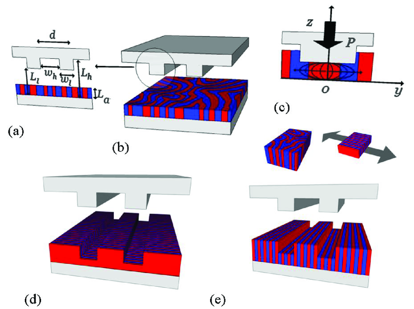
Nano Imprint Lithography (NIL) has been proposed in the mid-nineties9 and consists in first embossing a molten polymer film above its glass transition temperature with a mold exhibiting micro-scale features (Fig. 1), which is produced only once but can be re-used over 1000 times. Then, the combined substrate/film/mold is cooled down below and the film is separated from the weakly adhering fluorocarbon-coated mold. NIL has been widely used for homopolymers10; 11. However, BCP films were studied only in a few cases 12; 13; 14 and no attempt to organize defectless perpendicular structures over large distances (tens of micrometers) was reported. The ease of implementation and low cost of the method present tremendous advantages as compared to other techniques such as 193 nm deep UV, electron or focused ion beam lithography.15
In this work, we demonstrate how nano-rheology of the confined BCP film 7; 16; 17 and surface interactions due to the mold are used to control nano-structures, enabling unprecedented defect-free film ordering on the wafer scale. Hence, the flexibility of mold design provides an efficient top-down way to tailor BCP patterns transferrable onto a silicon substrate. In particular, NIL produces patterns in complex geometries that are hardly reachable using state-of-the-art fabrication methods, and can lead to a wealth of applications for integrated high-density devices such as magnetic memories, crossbar circuits and metamaterials.
Symmetric diblock copolymers of PS52K-b-PMMA52K with polydispersity index of 1.09 were purchased from Polymer Source Inc and exhibit a bulk lamellar phase of period nm 5. High-energy silicon wafers are cleaned and coated with a self-assembled monolayer (SAM) of octadecyltrichlorosilane. A UV/ozone treatment of the SAM is used to modify the surface energy and to induce perpendicular orientation of the BCP lamellae with respect to the substrate18. Finally, thin BCP films are spin-coated on the modified wafer, nanoimprinted and examined with SEM.
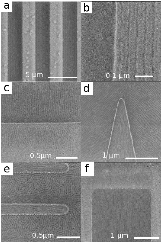
For samples processed at low temperatures of about C, defect-free lamellae having a periodicity of (Figs. 2 a and b) are observed and are oriented parallel to the groove edges over tens of micrometers. Self-consistent field theory (SCFT) calculations 19; 20 (see Supporting Information) in a three-dimensional geometry mimicking the experimental substrate and mold (Fig. 1) support the experimental findings and are shown in Fig. 3. This agreement between theory and experiment strengthens our claim that, in this low temperature case, the observed overall orientation is determined by the surface energy. Furthermore, if the substrate has no preference for one of the two blocks and the mold has a slight preference for one of them, well-ordered lamellae oriented perpendicular to the substrate and parallel to the grooves (Figs.2a, 2b and 3) are found. Indeed, for thin enough grooves in the direction (), the interaction with the mold side-walls prevails and is the main driving force for the orientation of the lamellae.20
Surprisingly, for samples processed at higher temperatures of around 170∘ C the lamellae are found to be perpendicular to the groove edges (Fig. 2c). This finding cannot be solely explained by equilibrium film considerations. The organization of BCP around a mold tip (Fig. 2d) suggests similar directed flow streamlines and points to important rheological effects that have been previously noticed for cylinders oriented parallel to the substrate14.
The rheology of BCP melts has attracted considerable attention since the 1970’s due to its particular relevance to extrusion 17; 21. Using the lubrication approximation (see Supporting Information), the film flow is expressed in terms of the shear rate , which is proportional to , where is the applied pressure, the initial film thickness, the film viscosity, and the distance from the zero velocity plane (Fig. 1c). The maximum shear rate is obtained at the groove walls and (). For low shear rates (less than s-1), it was shown both in experiments21; 22 and in numerical simulations23; 24 that the lamella normals are parallel to the shear gradient; namely, the lamellae are expected to be parallel to the substrate.
However, for higher shear rates the orientation of the lamella normals is perpendicular both to the shear gradient and to the flow direction, meaning that the lamellae are perpendicular to both the substrate and groove walls. With typical thickness and width values, =50 nm, =500 nm, and applied pressure Pa, we estimate the maximum shear rate to be s-1 at 110∘ C (viscosity Pa.s) and s-1 at 170∘ C ( Pa.s). This means that a lamellar orientation perpendicular to the groove walls is expected at 170∘ C, as it is indeed observed (Figs. 2c, 2d and 4)
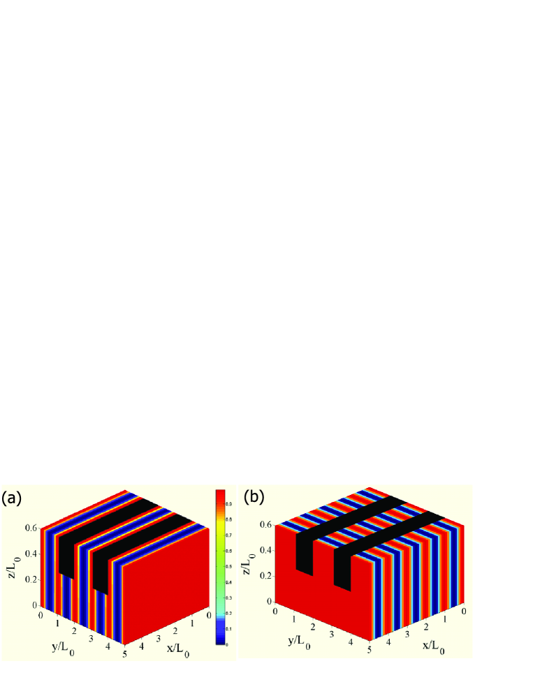
Full three-dimensional SCFT calculations show that a lamellar orientation parallel to the grooves is obtained when the film initial condition is in the disordered state (above ODT) (Fig. 3a). However, when we take the lamellae to be oriented perpendicular to the grooves as an initial condition which mimicks the polymer flow, the system keeps this orientation although it has a higher free energy (Fig. 3b). This suggests that a perpendicular orientation is not eventually destroyed by surface energy but rather is a metastable state of the system. We conclude that both film nano-rheology and surface energy are important in determining the BCP organization as shown in (Fig. 2e). In this latter case, the small width of the grooves implies a relatively large contribution to the surface energy of the vertical walls, leading to parallel orientation inside the grooves, whereas random orientation (with a preference to perpendicular orientation) is found close to the groove walls.
The competing effects of surface energy and nano-rheology provide a unique way to control and design nano-structures on silicon wafers. Large scale defect-free orientation of the lamellae can be reached by using a dedicated mold geometry to control the flow. This can be achieved by injecting polymer with large shear rate into the mold grooves in places where an orientation of the lamellae perpendicular to the walls is desired, while reducing the polymer flow in places where parallel orientation is needed. This is illustrated in Fig. 2f where the polymer flows from the lighter colored thinner regions to the central darker and thicker one. The upper downward flow reaches the thicker zone with a much higher shear rate than the lateral flow because the upper injection region has a much larger extension than the lateral ones (the shear rate increases with the coordinate, see Eq.(4) in SI). Surface energy effects are designed to reinforce the flow effect since the lateral side walls were made longer than the upper wall.
Flow is in fact particularly efficient for obtaining defect-free structures because of its long-range effect while surface energies represent a short-range one. Moreover, as the viscosity and shear rate can be varied over orders of magnitude ( to Pa.s.) by changing the temperature over C only, both effects can be furthermore combined. In Fig. 2f a high-temperature step causing defect healing was added to a low-temperature step used for pre-ordering at the walls. Namely, after a first step of 2 minutes at C for evaporating fully the solvent, a pre-ordering step was performed at C for 7 hours followed by a defect healing step at C for 72 hours. A force of 10 kN was applied onto the 4 inches wafer.
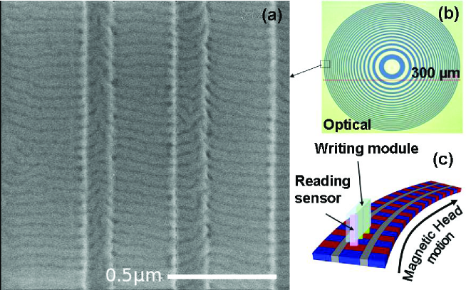
Our NIL method provides a versatile approach to order BCP nanostructures in various geometries. In Fig. 4 we show a radial ordering which is induced by a flow in a system of cylindrical symmetry. A mold with concentric grooves features was created and is shown in Fig. 4b. The remarkable radial ordering of the lamellae was obtained by a high temperature step to favor long-range ordering by the flow. This possibility of imprinting circular geometries is of great advantage for applications such as circular reading tracks for ultra-high density bit patterned media (BPM) proposed for magnetic storage disks25. Our present scheme can indeed create ultra-dense circular features (the density is fully tunable by the polymer molecular weight) perpendicular to a magnetic head motion (Fig. 4c). This is fully compatible with actual rotating magnetic disk, unlike other approaches that lead to patterns that are orthogonal in the - directions.
In conclusion we have demonstrated a simple way to generate and tailor defect-free nanostructures at the 10 nm resolution. Long-range nano-rheology and shorter-range surface energy effects can be efficiently combined to provide dedicated pattern geometries. For further applications the BCP patterns processed by NIL will play the role of an intermediate mask or of a template. We have successfully checked that such a BCP film can be transferred onto a silicon wafer by Reactive Ion Etching (see Supporting Information). In the future we foresee that metals can also be included into BCP structures using, for example, deposition of metallic layers onto pre-patterned templates26, electrodeposition27 and immersion in aqueous metal-salt solution28. When processed by our cost-effective NIL method, hybrid ordered nanostructures could provide a wealth of applications for ultra-high density magnetic recording media27, metal nano-structures for metamaterials and plasmonic circuits, sensors29 and memories30.
Experimental
Surface Modification of Silicon Substrates: Silicon wafers (p-type, 500 thick, purchased from MEMC Elect. Materials) were cleaned by sonication in purified Millipore water and 2-propanol, followed by exposure to UV under an oxygen atmosphere for 30 min. The cleaned wafers were silanized in a 2mM solution of octadecyltrichlorosilane (OTS) in heptane for 1 day. The wafers were put onto a heat plate at C for 5 min, then sonicated in toluene and dried with nitrogen before UV/ozone treatment.
Surface Energy Control: The SAM is subsequently oxidized to obtain the desired surface-energy value through UV/ozone treatment as previously shown in earlier work 18.
Polymer Film Deposition : 1 wt % solution of diblock copolymer of PS52K-b-PMMA52K, (Polymerization index:1.09) of symmetric composition (purchased from Polymer Source Inc.) in toluene was spin coated at 1800 rpm onto the silanized silicon wafer, in order to produce a BCP films with thickness of about 40-50 nm. Subsequently, the samples were annealed in a vacuum oven with a pressure less than 30 mbar at C for 1 day.
NanoImprinting Procedure :
Imprint experiments have been carried out using an EVG@520HE press under vacuum of about 0.1 mbar. The mold used was a 4in. silicon wafer with engraved nano-structures of 50 nm in height and between 250 nm and 8 m in width. An overall pressure of 1.5 MPa was then applied to all samples at temperatures of C (samples of Figs. 2a and 2b) or C (samples of Figs. 2c-2e) during 18h.
Critical Dimension Scanning Electron Microscopy (CD-SEM) were performed using a Hitachi 9300 instrument operating at low voltage (500 V).
Acknowledgements
Funding from Chimtronique and Nanosciences programs of the CEA, the network for advanced research “Triangle de la Physique” (POMICO project), the U.S.-Israel Binational Science Foundation under Grant No. 2006/055, the Israel Science Foundation under Grant No. 231/08, and the Center for Nanoscience and Nanotechnology at Tel Aviv University is gratefully acknowledged.
References
- [1] Bates, F. and Fredrickson, G. ‘Block copolymers - Designer soft materials.’ Physics Today, 52, 32–38 (1999).
- [2] Kellogg, G., Walton, D., Mayes, A., Lambooy, P., Russell, T., Gallagher, P., and Satija, S. ‘Observed surface energy effects in confined diblock copolymers.’ Physical Review Letters, 76, 2503–2506 (1996).
- [3] Bang, J., Jeong, U., Ryu, D. Y., Russell, T. P., and Hawker, C. J. ‘Block Copolymer Nanolithography: Translation of Molecular Level Control to Nanoscale Patterns.’ Advanced Materials, 21, 4769–4792 (2009).
- [4] Ruiz, R., Sandstrom, R. L., and Black, C. T. ‘Induced orientational order in symmetric diblock copolymer thin films.’ Advanced Materials, 19, 587 (2007).
- [5] Stoykovich, M., Muller, M., Kim, S., Solak, H., Edwards, E., de Pablo, J., and Nealey, P. ‘Directed assembly of block copolymer blends into nonregular device-oriented structures.’ Science, 308, 1442–1446 (2005).
- [6] Cheng, J. Y., Rettner, C. T., Sanders, D. P., Kim, H.-C., and Hinsberg, W. D. ‘Dense self-assembly on sparse chemical patterns: Rectifying and multiplying lithographic patterns using block copolymers.’ Advanced Materials, 20, 3155–3158 (2008).
- [7] Ruiz, R., Ruiz, N., Zhang, Y., Sandstrom, R. L., and Black, C. T. ‘Local defectivity control of 2D self-assembled block copolymer patterns.’ Advanced Materials, 19, 2157 (2007).
- [8] Segalman, R., Yokoyama, H., and Kramer, E. ‘Graphoepitaxy of spherical domain block copolymer films.’ Advanced Materials, 13, 1152 (2001).
- [9] Chou, S., Krauss, P., and Renstrom, P. ‘Imprint of sub-25 nm vias and trenches in polymers.’ Applied Physics Letters, 67, 3114–3116 (1995).
- [10] Li, M., Wang, J., Zhuang, L., and Chou, S. ‘Fabrication of circular optical structures with a 20 nm minimum feature size using nanoimprint lithography.’ Applied Physics Letters, 76, 673–675 (2000).
- [11] Jung, G., Ganapathiappan, S., Ohlberg, D., Olynick, Y., D.L. Chen, Tong, W., and R., S. ‘Fabrication of a 34 x 34 crossbar structure at 50 nm half-pitch by UV-based nanoimprint lithography.’ Nano Letters, 4, 1225–1229 (2004).
- [12] Li, H. and Huck, W. ‘Ordered block-copolymer assembly using nanoimprint lithography.’ Nano Letters, 4, 1633–1636 (2004).
- [13] Kim, S., Lee, J., Jeon, S.-M., Lee, H. H., Char, K., and Sohn, B.-H. ‘Orientation of lamellar nanostructures in the patterned thin films of a diblock copolymer.’ Macromolecules, 41, 3401–3404 (2008).
- [14] Voet, V., Pick, T., Park, S.-M., Moritz, M., Hammack, A., Urban, D., Ogletree, D., Olynick, D., and Helm, B. ‘Interface Segregating Fluoralkyl-Modified Polymers for High-Fidelity Block Copolymer Nanoimprint Lithography.’ Journal of the American Chemical Society, 133, 2812–2815 (2011).
- [15] Lithography,(Ed: S. Landis), Wiley, Chichester, UK (2010).
- [16] Sundrani, D. and Sibener, S. ‘Spontaneous spatial alignment of polymer cylindrical nanodomains on silicon nitride gratings.’ Macromolecules, 35, 8531–8539 (2002).
- [17] Angelescu, D., Waller, J., Adamson, D., Deshpande, P., Chou, S., Register, R., and Chaikin, P. ‘Macroscopic orientation of block copolymer cylinders in single-layer films by shearing.’ Advanced Materials, 16, 1736 (2004).
- [18] Liu, P. H., Thebault, P., Guenoun, P., and Daillant, J. ‘Easy Orientation of Diblock Copolymers on Self-Assembled Monolayers Using UV Irradiation.’ Macromolecules, 42, 9609–9612 (2009).
- [19] Man, X. K., Andelman, D., and Orland, H. ‘Block Copolymer at Nano-Patterned Surfaces.’ Macromolecules, 43, 7261–7268 (2010).
- [20] Man, X. K., Andelman, D., Orland, H., Thébault, P., Liu, P.-H., Guenoun, P., Daillant, J., and Landis, S. ‘Organization of Block Copolymers using NanoImprint Lithography: Comparison of Theory and Experiments.’ Macromolecules, 44, 2206-2211 (2010).
- [21] Hamley, I. W. ‘Structure and flow behaviour of block copolymers.’ J. Physics-condensed Matter, 13, R643–R671 (2001).
- [22] Chen, Z., Kornfield, J., Smith, S., Grothaus, J., and Satkowski, M. ‘Pathways to macroscale order in nanostructured block copolymers.’ Science, 277, 1248–1253 (1997).
- [23] Fraser, B., Denniston, C., and Muser, M. H. ‘On the orientation of lamellar block copolymer phases under shear.’ J. Chem. Phys., 124 (2006).
- [24] Lisal, M. and Brennan, J. K. ‘Alignment of lamellar diblock copolymer phases under shear: Insight from dissipative particle dynamics simulations.’ Langmuir, 23, 4809–4818 (2007).
- [25] Landis, S., Rodmacq, B., Dieny, B., Dal’Zatto, B., Tedesco, S., and Heitzmann, M. ‘Domain structure of magnetic layers deposited on patterned silicon.’ Applied Physics Letters, 75, 2473–2475 (1999).
- [26] Lu, J., Chamberlin, D., Rider, D. A., Liu, M. Z., Manners, I., and Russell, T. P. ‘Using a Ferrocenylsilane-Based Block Copolymer as a Template to Produce Nanotextured Ag Surfaces: Uniformly Enhanced Surface Enhanced Raman Scattering Active Substrates.’ Nanotechnology, 17, 5792–5797 (2006).
- [27] Thurn-Albrecht, T., Schotter, J., Kästle, G., Emley, N., Shibauchi, T., Krusin-Elbaum, L., Guarini, K., Black, C., Tuominen, M., and Russell, T. ‘Ultrahigh-Density Nanowire Arrays Grown in Self-Assembled Diblock Copolymer Templates.’ Science, 290, 2126–2129 (2000).
- [28] Chai, J., Wang, D., Fan, X., and Buriak, J. M. ‘Assembly of aligned linear metallic patterns on silicon.’ Nature Nanotechnology, 2, 500–506 (2007).
- [29] Mistark, P. A., Park, S., Yalcin, S. E., Lee, D. H., Yavuzcetin, O., Tuominen, M. T., Russell, T. P., and Achermann, M. ‘Block-Copolymer-Based Plasmonic Nanostructures.’ ACS Nano, 3, 3987–3992 (2009).
- [30] Hong, A. J., Liu, C.-C., Wang, Y., Kim, J., Xiu, F., Ji, S., Zou, J., Nealey, P. F., and Wang, K. L. ‘Metal Nanodot Memory by Self-Assembled Block Copolymer Lift-Off.’ Nano Letters, 10, 224–229 (2010).