Temperature Dependent Empirical Pseudopotential Theory For Self-Assembled Quantum Dots
Abstract
We develop a temperature dependent empirical pseudopotential theory to study the electronic and optical properties of self-assembled quantum dots (QDs) at finite temperature. The theory takes the effects of both lattice expansion and lattice vibration into account. We apply the theory to the InAs/GaAs QDs. For the unstrained InAs/GaAs heterostructure, the conduction band offset increases whereas the valence band offset decreases with increasing of the temperature, and there is a type-I to type-II transition at approximately 135 K. Yet, for InAs/GaAs QDs, the holes are still localized in the QDs even at room temperature, because the large lattice mismatch between InAs and GaAs greatly enhances the valence band offset. The single particle energy levels in the QDs show strong temperature dependence due to the change of confinement potentials. Because of the changes of the band offsets, the electron wave functions confined in QDs increase by about 1 - 5%, whereas the hole wave functions decrease by about 30 - 40% when the temperature increases from 0 to 300 K. The calculated recombination energies of exciton, biexciton and charged excitons show red shifts with increasing of the temperature, which are in excellent agreement with available experimental data.
pacs:
68.65.Hb, 73.22.-f, 78.67.HcI Introduction
During the past two decades, enormous progress has been achieved in understanding the electronic and optical properties of self-assembled quantum dots (QDs) both through theory and experiments, stimulated by their potential applications in QDs laser at room temperature, Tsu and Esaki (1973); Arakawa and Sakaki (1982); Kirstaedter et al. (1994) and as qubits and quantum photon emitters at low temperature. Imamoglu and Yamamoto (1994); Lounis and Orrit (2005); Benson et al. (2000); Stevenson et al. (2006); Akopian et al. (2006) For the former applications, it generally requires high density and highly uniform QDs. The QD laser has been demonstrated with much lower threshold current and much higher material and differential gains as compared to the semiconductor quantum well lasers. Ledentsov et al. (2000) For the latter applications, the preparation of single QD is crucial. A number of methods have demonstrated the feasibility to isolate single QD from QDs ensemble. Bayer et al. (2001); Marzin et al. (1994); Yamauchi et al. (2005); Tang et al. (2009) Rabi oscillation of exciton and charged exciton Kamada et al. (2001); Xu et al. (2008) in single QD have been observed experimentally, showing that the charge and spin quantum states in single QD can be coherently controlled via optical method. The single and entangled photon emission from single QD have also been demonstrated experimentally, Shields (2007) that are much brighter Dousse et al. (2010) than the traditional parameter-down entangled photon source. Shih and Alley (1988); Kiess et al. (1993) These experimental achievements pave the way for future application of QDs in quantum computation.
On the other hand, the development of the atomistic theories, including the empirical pseudopotential method Zunger (2001); Wang et al. (1999); Wang and Zunger (1999) and the tight-binding models Zieliński et al. (2010); Lee et al. (2001); Santoprete et al. (2003) provide deep insight to the electronic and optical properties of self-assembled QDs. The atomistic theories of QDs not only give results that agree well with experiments, Ding et al. (2010); Singh and Bester (2009); Ediger et al. (2007a, b) but also greatly improve our understanding of the properties of QDs. The atomistic models capture the correct point group symmetry of the QDs, which is missing in the continuum model. Therefore they can give correct interpretation of some subtle properties of the QDs, e.g., the fine structure splitting (FSS), Bester et al. (2003) and light polarization of excition. Gong et al. (2011) Unfortunately, so far all the theories of QDs have been restricted to zero temperature.
Temperature is a very important degree of freedom in experiments to tune the electronic and optical properties of QDs. For example, in QDs laser, the temperature has be used to tune the laser wavelength. Tsu and Esaki (1973); Arakawa and Sakaki (1982); Kirstaedter et al. (1994) In the QD-cavity system, the temperature is generally used to tune the resonance between the QDs and the cavity in order to achieve strong coupling between the two quantum systems. Loo et al. (2010); Press et al. (2007); Laussy et al. (2008); Englund et al. (2007) The temperature dependent optical spectra of (single and ensemble) QDs have been investigated intensively in experiments in the past decades. Ortner et al. (2005); Gong et al. (2010); Ortner et al. (2005); Bayer et al. (2001); Marzin et al. (1994); Yamauchi et al. (2005); Kamada et al. (2001); Xu et al. (2008); Yeo et al. (2011) New physics, for example, the formation of excitonic polaronGong et al. (2010); Hameau et al. (1999); Preisler et al. (2005) which is due to strong coupling between exciton and optical phonons, may be found in QDs at high temperature. However, a theoretical understanding of the temperature effects in QDs is still missing. Therefore, to facilitate the future device applications of QDs, the development of a temperature dependent theory is not only of theoretical interest, but also of practical importance.
In this work, we develop such a temperature dependent atomistic pseudopotential theory to study the electronic and optical properties of QDs at finite temperature. We take the effects of both lattice expansion and lattice vibration into account. The latter is done by introducing a temperature dependent dynamical Debye-Waller factor to the structure factor. We first examine the temperature dependent electronic structures of bulk InAs and GaAs, and then apply the theory to investigate the electronic and optical properties of self-assembled InAs/GaAs QDs. The calculated temperature dependent photoluminescence (PL) spectra of QDs are in excellent agreement with available experimental data.
The rest of the paper is organized as follows. In Sec. II we introduce the temperature dependent empirical pseudopotential method (TDEPM). In Sec. III, we study the electronic structures of bulk InAs, GaAs using TDEPM, including the energy band gaps and band offsets, etc. We present the temperature dependent band offsets for InAs/GaAs QDs in Sec. IV.1 and the single particle energy levels and wave functions of InAs/GaAs QDs in Sec. IV.2. We discuss the temperature dependent optical spectra of InAs/GaAs QDs in Sec. IV.3, and summarize in Sec. V.
II Methodology
We consider InGaAs QDs embedded in the center of a 60 60 60 GaAs 8-atom unit cell. Periodic boundary condition is used to obtain the single particle energy levels. To study the electronic and optical properties of the QDs at finite temperature, we introduce temperature dependent pseudopotentials in the single-particle Hamiltonian,
| (1) |
where is the strain dependent screened empirical pseudopotential for atom of type and atom index at temperature . is the optimized atom position from valance force field (VFF) method. Keating (1966); Martin (1970) In a strained lattice, the atomic potential is assume to have the form of,
| (2) |
where is the local hydrostatic strain at . is fitted to the deformation potentials of the bulk materials. The atomistic theory naturally captures the correct point group symmetry of the QDs even at high temperature.
The effects of lattice vibration can be taken into account using Brooks-Yu theory, Yu and Brooks (1964) which has been applied to study the energy gap of bulk materials in the context of pseudopotentials. Keffer et al. (1968, 1970); Skelton et al. (1972); Guenzer and Bienenstock (1973) The total atomic potential at temperature , which is the sum of all atomic potentials , can be written as,
| (3) | |||||
where is the reciprocal lattice vector. is the Fourier transform of the screened atomistic potential at zero temperature, which takes the form of, Williamson et al. (2000)
| (4) |
where , and the parameters , , , are fitted to the bulk properties of InAs and GaAs, including the band gaps, band offsets, effective masses, etc. is the averaged structure factor over all the phonon configurations at temperature ,
| (5) |
Assuming , where is the amplitude of the phonon mode. For any , we have
| (6) |
using Wick’s theorem. Marder (1999) Therefore, the temperature effects to the atomic potentials are equivalent to consider a temperature dependent structure factor,
| (7) |
in Eq. 3, where is the dynamical Debye-Waller factor for the -th element,
| (8) |
For simplicity, we assume the system to be isotropic, then we have
| (9) |
where is the total mean-square displacement for atom of type at temperature , including the contribution from acoustic (A) and optical (O) phonons,
| (10) |
We use Debye model for acoustic phonons,
| (11) | |||||
where , and is the Debye temperature. The second term in the bracket is from zero point quantum fluctuation, which can be absorbed to the zero-temperature pseudopotentials. At high temperature, the acoustic phonon displacement , whereas in the low-temperature limit, . For the optical phonons, the average displacement can be written as
| (12) |
where is the frequency of the optical phonon. We neglect the dispersion of optical phonons here. Generally, the contribution of the optical phonon could be significant only at high temperature. Fan (1951) Although and can be calculated directly using the parameters of bulk materials, the approximations made during the derivations of Eq. (11) and (12) can introduce some errors to the energy gap of semiconductors at finite temperature. To overcome this problem, we treat and as fitting parameters, which are fitted to the temperature dependent band structures in combination with the zero-temperature empirical pseudopotentials. Therefore, the dynamical Debye-Waller factors might be different from the real physical Debye-Waller factors of the system.
| GaAs | InAs | ||||
|---|---|---|---|---|---|
| Property | EPM | Expt. | EPM | Expt. | |
| 1.528 | 1.52 | 0.423 | 0.42 | ||
| -2.763 | -2.96 | -2.365 | -2.40 | ||
| 1.937 | 1.98 | 2.069 | 2.34 | ||
| 2.232 | 2.50 | 2.514 | 2.54 | ||
| -1.041 | -1.30 | -0.872 | -1.26 | ||
| 2.232 | 1.81 | 1.568 | 1.71 | ||
| 0.067 | 0.067 | 0.023 | 0.023 | ||
| 0.316 | 0.40 | 0.371 | 0.35 | ||
| 0.825 | 0.57 | 0.986 | 0.85 | ||
| 0.092 | 0.082 | 0.029 | 0.026 | ||
| -7.879 | -8.33 | -6.804 | -5.7 | ||
| -1.110 | -1.0 | -0.829 | -1.0 | ||
| -1.567 | -1.7 | -1.631 | -1.7 | ||
| 0.362 | 0.34 | 0.384 | 0.39 | ||
| 0.201 | 0.22 | 0.286 | 0.27 | ||
| parameters | Ga | As (GaAs) | In | As (InAs) |
|---|---|---|---|---|
| 476845.70 | 11.9753 | 771.3695 | 26.8882 | |
| 1.9102 | 3.0181 | 1.6443 | 2.9716 | |
| 22909.50 | 1.1098 | 18.1342 | 1.2437 | |
| 0.1900 | 0.2453 | 0.3940 | 0.4276 | |
| 2.5215 | 0.0 | 2.1531 | 0.0 | |
| 0.1035 | 0.0976 | 0.5973 | 0.0976 |
| cation | anion | |||||
|---|---|---|---|---|---|---|
| Bulk | (K) | (meV) | ||||
| GaAs | 344 | 35.36 | 0.3024 | 0.0786 | 0.1530 | 0.0024 |
| InAs | 247 | 29.6 | 0.1014 | 0.0984 | 0.0828 | 0.0084 |
To determine the temperature dependent pseudopotential, we first determine the pseodupotential parameters - and at zero temperature by fitting them to the electronic structures of bulk materials, including the effective mass, and energies of the high symmetry , and points, etc. The target values and fitted values for GaAs and InAs are compared in Table 1, which are in good agreement. The parameters - and are presented in Table 2. With these parameters at hand, we then determine the values of and by fitting them to the temperature dependent energy gap of bulk materials, which can be well described by the empirical Varshni formula, Vurgaftman and Meyer (2001); Pässler (2003)
| (13) |
where and are the Varshni parameters. For GaAs, = 0.5405 meV/K and = 204 K and for InAs, = 0.276 meV/K and = 93 K.Vurgaftman and Meyer (2001) The fitted parameters for and are summarized in Table. 3.
The single-particle Hamiltonian (1) can be solved by expanding the wave functions into a linear combination of Bloch bands (LCBB), Wang and Zunger (1999)
| (14) |
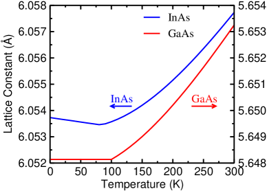
where is the bulk Bloch bands with orbital and wave vector close to point at finite temperature , and = (InAs, GaAs). The experimental lattice constants for InAs and GaAs at given temperature, as shown in Fig. 1, are given as input to construct the Bloch basis. At each temperature, we relax the dot+matrix structure using VFF method to get the the atomic position .
Due to the spatial confinement, the carries in the QDs have strong Coulomb interactions. The many-particle Hamiltonian read as,
| (15) |
where is the field operator with corresponding single particle energy . are the Coulomb integrals,
| (16) |
Here, is the screened dielectric function. Franceschetti et al. (1999) The many-particle Hamiltonian is solved using a configuration interaction method, Franceschetti and Zunger (2000) where the many-particle wave functions are expanded on the Slater determinants constructed from the confined electron and hole levels. This method has been successfully applied to studying the electronic and optical properties of InAs/GaAs QDs and the obtained results are in very good agreement with the experimental observations. Ding et al. (2010); Ediger et al. (2007a, b); Williamson et al. (2000)
III TDEPM For Bulk Materials
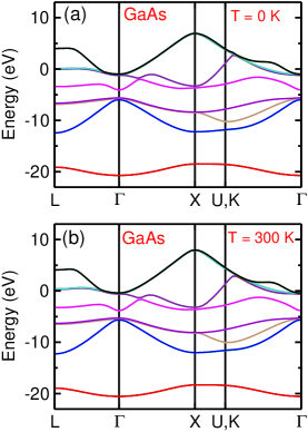
We first test our method for bulk materials. Figure 2 depicts typical band structures of GaAs at T = 0 and T = 300 K. The overall band structures are quite similar to those at zero temperature even at rather high temperature (300 K). However, the energies of high symmetry -points , , and have different response to the temperature. In principle, all the energies of these -points should be taken as the target values to determine the values of and . Unfortunately, the experimental data of the energies of these -points at finite temperature are not available, therefore, tentatively, we fit the potentials only to the temperature dependent energy gaps at point. The potentials can be improved by fitting to the energies of more -points in the future.
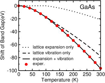
We present in Fig. 3 the change of energy gap as a function of temperature for GaAs. The filled circles are the results taken from experiments, Vurgaftman and Meyer (2001) whereas the solid line is calculated from TDEPM. The fitting error is less than 0.2 meV in the whole temperature range. The dashed line is the change of energy gap of GaAs taken account only lattice vibration, whereas the dotted line is the result with only lattice expansion. As we see, to accurately describe the red shift of the band gap with respect to temperature, both the lattice expansion and lattice vibration have to be taken into account in the theory. These results agree with the results obtained from temperature dependent tight-binding method by Pour et al. Pour et al. (2011) Similar features are also found for InAs using the parameters given in Table 3.
The conduction band offset () and valance band offset () between InAs and GaAs, defined as
| (17) |
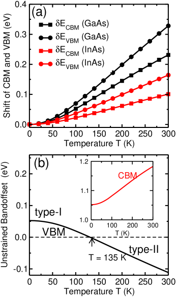
are very important to the electronic structures of the InAs/GaAs heterostructures, because they are important for the confinement of electron and hole in InAs/GaAs QDs. We show the change of CBM and VBM of InAs and GaAs with temperature in Fig. 4 (a), and the temperature dependent band offsets between InAs and GaAs in Fig. 4 (b). We find:
(i) The CBM and VBM of GaAs change much larger than their counterparts in InAs.
(ii) The CBM generally changes much larger than VBM. At high temperature ( 100 K), CBM and VBM change approximately linearly with respect to temperature. The changes of the band offsets with respect to the temperature are presented in Fig. 4 (b) for the VBM and in the inset for CBM. For electron, the temperature effect generally enhances the band offset, whereas for hole, the band offset decreases with the increasing of the temperature. Interestingly, there is a type-I to type-II transition at = 135 K for unstrained InAs/GaAs. However, becauase of the strain effects, the holes are still localized in InAs/GaAs QDs (see Sec. IV). In what follows we will show that the change of band offsets at finite temperature will greatly modify the electronic and optical properties of QDs.
IV TDEPM For InAs/GaAs QDs
| # | Base (nm) | Height (nm) | |
|---|---|---|---|
| QD-A | 1.0 | 25 | 3.5 |
| QD-B | 0.6 | 25 | 3.5 |
| QD-C | 0.7 | 25 | 3.5 |
| QD-D | 0.8 | 25 | 3.5 |
| QD-E | 1.0 | 25 | 5.5 |
| QD-F | 0.6 | 25 | 5.5 |
| QD-G | 0.7 | 25 | 5.5 |
| QD-H | 0.8 | 25 | 5.5 |
In Sec. III, we study the temperature dependent electronic structures of bulk InAs and GaAs. The band offsets between InAs and GaAs are greatly modified due to the temperature effects and there is a type-I to type-II transition in the unstrained InAs/GaAs heterostructure. The change of band offsets will significantly change the corresponding electronic and optical properties in QDs. However, the temperature dependent properties are more complicated in QDs because of the strain effects. In this section, we investigate the temperature dependent electronic and optical properties of InAs/GaAs QDS using TDEPM. We study QDs with different sizes and alloy compositions. The alloy compositions of selected lens-shaped QDs are presented in Table 4. In most of the cases, we use QD-A to illustrate the main physics. The results of other QDs will also be presented for comparison.
IV.1 Temperature dependent band offset
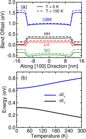
We first investigate the strained band offsets in InAs/GaAs QDs, which is crucial for the electronic and optical properties of QDs. In previous works, He et al. (2004); Gong et al. (2008) the Bir-Pikus model is used to obtain the strain modified band profiles. However, the temperature dependent parameters for the Bir-Pikus model is generally unavailable. Therefore, we calculate the band profiles directly using the TDEPM. After the lattice relaxations for the dot system, we construct the 8-atom unit cell according to the local strain, and then calculate the band structures using the TDEPM. Typical band offsets in InAs/GaAs dots along the [100] direction at K is compared to those of zero temperature in Fig. 5 (a). We see that the overall profiles of the heave hole (HH) and light hole (LH) and spin-orbit (SO) bands are still quite similar at the two temperatures. The SO band is lower than the HH and LH by about 400 meV in the matrix and is greatly enhanced in the dot materials. The degeneracy of the HH and LH bands is broken because of the biaxial strain. He et al. (2004); Wei and Zunger (1994) The strained band offsets of CBM and VBM in the center of InAs/GaAs QDs are presented in Fig. 5 (b) in the temperature range of 0 - 300 K. For electrons, the confinement is enhanced with increasing of the temperature, whereas for holes, the confinement decreases from 320 to 180 meV. However, unlike the bulk materials, even at high temperature, is always positive, indicating that the hole is always localized in the QDs. The change of the band offsets greatly modifies the electronic and optical properties of QDs, as shall be discussed below.
IV.2 Temperature dependent single particle levels and wave functions
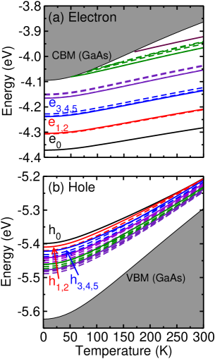
The evolution of single particle energy levels as functions of temperature is illustrated in Fig. 6. We show the results for QD-A here. Similar features are also found for all other QDs. We show all confined electron states, and the highest 20 hole states. Because of the enhancement of confinement potential for electrons, more states are confined in the dots as the increasing of the temperature. The labels of ( represent the energy levels of electron (hole) in ascending (descending) order. One can also use angular momentum , , , etc. to label the wave functions. For instance, the states and can be labeled as and the () states are usually labeled by , etc.
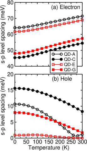
The - energy level spacing is shown in Fig. 7, which is defined as,
| (18) |
for both electrons and holes. Because of the increase of confinement potential, the electron - level spacing increases with the increasing of the temperature. In contrast, for holes, the energy level spacings decreases with the increasing of the temperature due to the decrease of the hole confinement potential. For QD-A, we find that the level spacing of electron increases from 64 to 70 meV when the temperature increases from 0 K to 300 K. For hole, the energy difference decreases from 11 to about 1 meV. The change of level spacings in QDs may be measured from PL emission spectra.
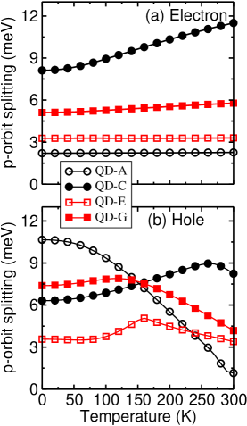
The -orbit splitting is another important quantity for the single particle levels, which is defined as,
If the QDs have or symmetry, the -orbit splitting is exactly zero. However, for real QDs, the highest symmetry is , and in alloyed QDs, the symmetry is , the splitting is nonzero. The results of the -orbit splitting are presented in Fig. 8 for different types of QDs. For QD-A and QD-E, the electron -orbit splittings are almost independent of temperature, whereas for other two types of QDs the -orbit splittings slightly increase with the increasing of temperature. The results for holes are very different from those for electrons, as shown in Fig. 8 (b). Because the hole level spacings are very small and the anti-crossing between the hole levels may occur when increasing the temperature, the -level splittings are not monotonic functions of the temperature. At high temperature, the -level spacing may even exceed the - level spacing, which will never happen for electrons. The -orbit splitting can be measured experimentally via pump-probe spectroscopy.Zibik et al. (2004, 2009)
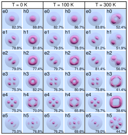
The change of confinement potentials may also change the shapes of the wave functions. We present the squared envelope wave functions of electrons and holes at = 0, 100 and 300 K in Fig. 9 for QD-A. The number on the lower right corner of each small panel represents the percentage of the density confined in the QDs. For , we find that the confined densities increase by about 1% - 2%, whereas for the higher states, the confined densities may increase about 4% - 5%. Although the electron squared wave functions confined in QDs slightly increase, their overall shapes hardly change. In contrast, for holes, the confined densities reduce dramatically when the temperature increases. For instance, the confined density decreases from 88.8% to 52.4% for when the temperature increases from 0 to 300 K. For , the confined density decreases from 76.8% to 44.7%. The shapes of the envelope functions for holes also change dramatically. For instance, the state is Gaussian-like at low temperature, but at high temperature there is a node at the center of the wave function. This change of the wave function is due to the enhancement of the interfacial effect in the QDs, because the confinement is very small for holes at high temperature. At low temperature only the tall QDs have such interfacial hole states. He et al. (2004); Gong et al. (2008) The change of the wave functions with respect to temperature can be measured experimentally using magnetotunneling spectroscopy. Bester et al. (2007); Vdovin et al. (2000)
IV.3 Temperature dependent PL emission spectrum

In this section, we investigate the temperature dependence of the optical spectra of InAs/GaAs QDs. The optical spectra of single InAs/GaAs QD Ortner et al. (2005); Bayer et al. (2001); Marzin et al. (1994); Yamauchi et al. (2005); Kamada et al. (2001); Xu et al. (2008) have been measured at low temperature. The highest measuring temperature as far as we know is up to 100 K, performed by Ortner et al.Ortner et al. (2005) At higher temperature, the signal to noise ratio may become very low and the single QD emission is usually hard to detect. However, for QDs ensemble, the emissions from QDs can be resolved even at room temperature. Therefore in this work, we study the optical spectra of QDs up to 300 K.
Figure 10 depicts the PL emission spectra of QD-A from 0 K to 300 K. The energy difference between and shell emission can be approximated by the sum of - single particle energy level spacing of electron and hole, i.e.
Although the change of level spacing in Fig. 7 can not been directly measured from PL emission spectra, the sum of them can be measured. The energy difference between and shells for QD-A is 80 meV at zero temperature and reduces to 72.5 meV at 300 K.
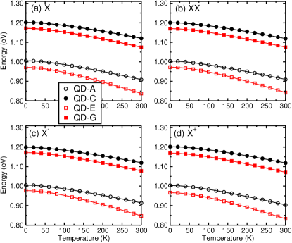
Figure 11 depicts the temperature dependent energies of the primary exciton, biexiciton and charged excitons for dots A, C, E, G. All the energies of exciton complexes show red shift as the temperature increases. For all dots, we find that the red shifts of the exciton complexes emission lines can be fitted very well using Varshni formula, with the fitting errors generally less than 1 meV. The fitting errors are slightly larger than that for the bulk materials ( 0.2 meV), but much smaller than the total red shift of the emission line which is about 100 meV. This suggests that the red shift of the emission energies is proportional to at low temperature. The values of the Varshni parameters are summarized in Table 5. These parameters are very different than those of bulk InAs, GaAs, and also vary from dot to dot.
| # | ||||||||||||
|---|---|---|---|---|---|---|---|---|---|---|---|---|
| QD-A | 1.0056 | 0.4861 | 151.2457 | 1.0038 | 0.4583 | 137.7505 | 1.0048 | 0.4451 | 139.6235 | 1.0031 | 0.5050 | 155.5669 |
| QD-B | 1.2600 | 0.4579 | 231.8752 | 1.2592 | 0.4500 | 217.6022 | 1.2568 | 0.4458 | 229.9588 | 1.2610 | 0.4605 | 217.5235 |
| QD-C | 1.2021 | 0.4419 | 187.7806 | 1.2007 | 0.4364 | 181.1664 | 1.1994 | 0.4266 | 182.4588 | 1.2021 | 0.4493 | 184.1575 |
| QD-D | 1.1109 | 0.4357 | 157.3439 | 1.1392 | 0.4275 | 151.4595 | 1.1387 | 0.4062 | 141.2489 | 1.1399 | 0.4503 | 161.8518 |
| QD-E | 0.9714 | 0.7165 | 180.7079 | 0.9725 | 0.7127 | 193.0234 | 0.9768 | 0.7148 | 195.3687 | 0.9663 | 0.7178 | 182.4702 |
| QD-F | 1.2322 | 0.4957 | 188.3547 | 1.2305 | 0.4854 | 182.7430 | 1.2312 | 0.4836 | 189.6459 | 1.2306 | 0.4994 | 183.6016 |
| QD-G | 1.1717 | 0.5017 | 165.5773 | 1.1702 | 0.4861 | 159.2807 | 1.1720 | 0.4800 | 159.7797 | 1.1691 | 0.5107 | 166.9354 |
| QD-H | 1.1085 | 0.5393 | 164.2455 | 1.1077 | 0.5151 | 155.4030 | 1.1102 | 0.5059 | 153.0005 | 1.1052 | 0.5424 | 161.4847 |
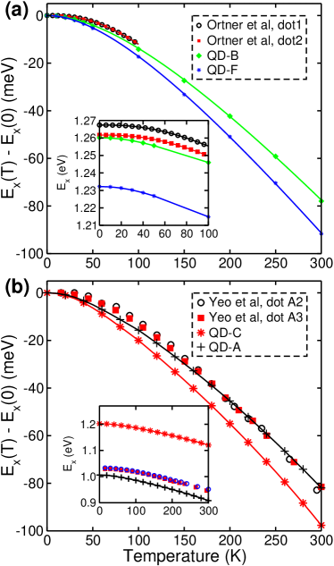
The temperature dependent optical spectra has been studied experimentally by several groups. Ortner et al. (2005); Yeo et al. (2011) For example, red shift of exciton emission line in single QDs have been investigated by Ortner et alOrtner et al. (2005) from = 0 K to = 100 K. In Fig. 12 (a), we compare our theoretical results (QD-B, QD-F) with the available experimental dataOrtner et al. (2005) for the In0.6Ga0.4As/GaAs QDs. The red shift of the emission line of exciton agree well with QD-B (less than 1 meV). In the inset of Fig. 12, we present the exciton energies as a functions of temperature, which also show excellent agreement. The red shift of exciton energy in Ref. Ortner et al., 2005 can be well described by Varshni formula using meV/K and K, with error less than 1 meV. This is also in a good agreement with the theoretical values for QD-B given in Table 5.
In Fig. 12 (b), we compare the theoretical results of QD-A and QD-C with the experimental results for QDs ensemble measured by Yeo et al. Yeo et al. (2011) where the peak energy of -shell is chosen as the exciton emission lines at each temperature. For QDs ensemble, the -shell can be well resolved even at room temperature. We see that the red shifts of QDs ensemble and agree well with the theoretical prediction of QD-A. Moreover, the exciton energy of and at zero temperature is around 1.02 - 1.03 eV, also agree well with the exciton energy of QD-A listed in Table 5.
We note that some experimentsCardona et al. (2004) suggest that the redshift of the exciton energies proportional to , Passler et al. (1999); Fernández et al. (1997) instead of as suggested by TDEPM at very low temperature ( K). The discrepancy may come from two reasons. First, it is because we do not have high accurate temperature dependent band gaps to fit at very low temperature at present stage. It may also partly comes from the approximations we made in deriving the temperature dependent pseudopotentials. Nevertheless, in this temperature range, the change of exciton energies is very small, and the difference between the experimental values and the theory is very subtle.
We also calculate the FSS and the polarization of the mono-exciton at finite temperatures. We find that the FSS and the polarization are generally insensitive to the temperature. For example, the change of FSS is usually less than 1 eV, and the change of polarization is less than 5 degree when increasing the temperature from 0 to 100 K. This result suggests that the FSS can not been tuned using temperature effect.
V Summary and Conclusions
We develop a temperature dependent empirical pseudopotential theory, and apply it to study the electronic and optical properties of self-assembled InAs/GaAs quantum dots (QDs) at finite temperature. The theory takes the effects of both lattice expansion and lattice vibration into account. The pseudopotentials correctly reproduce the temperature dependent band gap of bulk III-V semiconductors such as InAs, and GaAs, etc. We find that for the unstrained InAs/GaAs heterostructure, the conduction band offset increases whereas the valence band offsets decreases with the increasing of the temperature, and there is a type-I to type-II transition at approximately 135 K. Yet, for InAs/GaAs QDs, the holes are still localized in the QDs even at room temperature because the large lattice mismatch between InAs and GaAs greatly enhances the valence band offset. The single particle energy levels in the QDs show strong temperature dependence due to the change of confinement potentials. As a consequence, more electron states are confined at higher temperature. Because of the changes of the band offsets, the electron wave functions confined in QDs increase by about 1 - 5%, whereas the hole wave functions decrease by about 30 - 40% when the temperature increase from 0 to 300 K. The calculated recombination energies of exciton, biexciton and charged excitons show red shift with the increasing of the temperature, which are in excellent agreement with available experimental data. We expect the theory can facilitate the future device applications of QDs.
Acknowledgments. - LH acknowledges the support from the Chinese National Fundamental Research Program 2011CB921200, National Natural Science Funds for Distinguished Young Scholars and the Fundamental Research Funds for the Central Universities No. WK2470000006.
References
- Tsu and Esaki (1973) R. Tsu and L. Esaki, Appl. Phys. Lett. 22, 562 (1973).
- Arakawa and Sakaki (1982) Y. Arakawa and H. Sakaki, Appl. Phys. Lett. 40, 939 (1982).
- Kirstaedter et al. (1994) N. Kirstaedter, N. N. Ledentsov, M. Grudmann, D. B. V. Ustinov, S. Ruvimov, M. Maximov, P. K. andZ. Alferov, U. Richter, P. Werner, U. Gosele, et al., Electronics Letters 30, 1416 (1994).
- Imamoglu and Yamamoto (1994) A. Imamoglu and Y. Yamamoto, Phys. Rev. Lett. 72, 210 (1994).
- Lounis and Orrit (2005) B. Lounis and M. Orrit, Rep. Prog. Phys. 68, 1129 (2005).
- Benson et al. (2000) O. Benson, C. Santori, M. Pelton, and Y. Yamamoto, Phys. Rev. Lett. 84, 2513 (2000).
- Stevenson et al. (2006) R. M. Stevenson, R. J. Young, P. Atkinson, K. C. D. A. Ritchie, and A. J. Shields, Nature 439, 179 (2006).
- Akopian et al. (2006) N. Akopian, N. H. Lindner, E. Poem, Y. Berlatzky, J. Avron, D. Gershoni, B. D. Gerardot, and P. M. Petroff, Phys. Rev. Lett. 96, 130501 (2006).
- Ledentsov et al. (2000) N. N. Ledentsov, M. Grundmann, F. Heinrichsdorff, D. Bimberg, V. M. Ustinov, A. E. Zhukov, M. V. Maximov, and Z. I. A. J. A. Lott, IEEE J. Select. Topic Quantum Electron 6, 439 (2000).
- Bayer et al. (2001) M. Bayer, P. Hawrylak, K. Hinzer, S. andM. Korksinskl, Z. R. Wasllewski, O. Stern, and A. Forchel, Science 291, 451 (2001).
- Marzin et al. (1994) J.-Y. Marzin, J.-M. Gérard, A. Izraël, D. Barrier, and G. Bastard, Phys. Rev. Lett. 73, 716 (1994).
- Yamauchi et al. (2005) S. Yamauchi, K. Komori, I. Morohashi, K. Goshima, T.Sugaya, and T. Takagahara, Appl. Phys. Lett. 87, 182103 (2005).
- Tang et al. (2009) J.-S. Tang, C.-F. Li, M. Gong, G. Chen, Y. Zou, J.-S. Xu, and G.-C. Guo, Physica E: Low-dimensional Systems and Nanostructures 41, 797 (2009).
- Kamada et al. (2001) H. Kamada, H. Gotoh, J. Temmyo, T. Takagahara, and H.Ando, Phys. Rev. Lett. 87, 246401 (2001).
- Xu et al. (2008) X. Xu, B. Sun, P. R. Berman, D. G. S. andAllan S. Bracker adn Dan Gammon, and L. J. Sham, Nature Physics 4, 692 (2008).
- Shields (2007) A. J. Shields, Nat. Photon. 1, 215 (2007).
- Dousse et al. (2010) A. Dousse, J. Suffczyński, A. Beveratos, O. K. A. Lemaitre, I. Sagnes, J. Bloch, and P. V. andP. Senellart, Nature 466, 217 (2010).
- Shih and Alley (1988) Y. H. Shih and C. O. Alley, Phys. Rev. Lett. 61, 2921 (1988).
- Kiess et al. (1993) T. E. Kiess, Y. H. Shih, A. V. Sergienko, and C. O. Alley, Phys. Rev. Lett. 71, 3893 (1993).
- Zunger (2001) A. Zunger, phys stat. sol (b) 224, 727 (2001).
- Wang et al. (1999) L.-W. Wang, J. Kim, and A. Zunger, Phys. Rev. B 59, 5678 (1999).
- Wang and Zunger (1999) L.-W. Wang and A. Zunger, Phys. Rev. B 59, 15806 (1999).
- Zieliński et al. (2010) M. Zieliński, M. Korkusiński, and P. Hawrylak, Phys. Rev. B 81, 085301 (2010).
- Lee et al. (2001) S. Lee, L. Jönsson, J. W. Wilkins, G. W. Bryant, and G. Klimeck, Phys. Rev. B 63, 195318 (2001).
- Santoprete et al. (2003) R. Santoprete, B. Koiller, R. B. Capaz, P. Kratzer, Q. K. K. Liu, and M. Scheffler, Phys. Rev. B 68, 235311 (2003).
- Ding et al. (2010) F. Ding, R. Singh, J. D. Plumhof, T. Zander, V. K. rápek, Y. H. Chen, M. Benyoucef, V. Zwiller, K. Dörr, G. Bester, et al., Phys. Rev. Lett. 104, 067405 (2010).
- Singh and Bester (2009) R. Singh and G. Bester, Phys. Rev. Lett. 103, 063601 (2009).
- Ediger et al. (2007a) M. Ediger, G. Bester, A. Badolato, P. M. Petroff, K. Karrai, A. Zunger, and R. J. Warburton, Nature Physics 3, 774 (2007a).
- Ediger et al. (2007b) M. Ediger, G. Bester, B. D. Gerardot, A. Badolato, P. M. Petroff, K. Karrai, A. Zunger, and R. J. Warburton, Phys. Rev. Lett. 98, 036808 (2007b).
- Bester et al. (2003) G. Bester, S. Nair, and A. Zunger, Phys. Rev. B 67, 161306 (2003).
- Gong et al. (2011) M. Gong, W. Zhang, G.-C. Guo, and L. He, Phys. Rev. Lett. 106, 227401 (2011).
- Loo et al. (2010) V. Loo, L. Lanco, A. L. andIsabelle Sagnes, O. Krebs, P. Voisin, and PascaleSenellart, Appl. Phys. Lett. 97, 2411110 (2010).
- Press et al. (2007) D. Press, S. Götzinger, S. Reitzenstein, C. Hofmann, A. Löffler, M. Kamp, A. Forchel, and Y. Yamamoto, Phys. Rev. Lett. 98, 117402 (2007).
- Laussy et al. (2008) F. P. Laussy, E. delValle, and C. Tejedor, Phys. Rev. Lett. 101, 083601 (2008).
- Englund et al. (2007) D. Englund, A. Faraon, I. Fushman, N. S. P. Petroff, and J. Vuičković, Nature 450, 857 (2007).
- Ortner et al. (2005) G. Ortner, M. Schwab, M. Bayer, R. Pässler, S. Fafard, Z. Wasilewski, P. Hawrylak, and A. Forchel, Phys. Rev. B 72, 085328 (2005).
- Gong et al. (2010) M. Gong, G. Chen, L. He, C.-F. Li, J.-S. Tang, F.-W. Sun, Z.-C. Niu, S.-S. Huang, Y.-H. Xiong, H.-Q. Ni, et al., Europhysics Letters 90, 37004 (2010).
- Yeo et al. (2011) I. Yeo, J. D. Song, and J. Lee, Appl. Phys. Lett. 99, 151909 (2011).
- Hameau et al. (1999) S. Hameau, Y. Guldner, O. Verzelen, R. Ferreira, G. Bastard, J. Zeman, A. Lemaitre, and J. M. Gérard, Phys. Rev. Lett. 83, 4152 (1999).
- Preisler et al. (2005) V. Preisler, R. Ferreira, S. Hameau, L. A. de Vaulchier, Y. Guldner, M. L. Sadowski, and A. Lemaitre, Phys. Rev. B 72, 115309 (2005).
- Keating (1966) P. N. Keating, Phys. Rev 145, 637 (1966).
- Martin (1970) R. M. Martin, Phys. Rev. B 1, 4005 (1970).
- (43) O. Madelung, Semiconductors: Data Handbook 3rd Edition (Springer, 2003).
- Yu and Brooks (1964) S. C. Yu and H. Brooks, Tech. Rep., Harvard University (1964).
- Keffer et al. (1968) C. Keffer, T. M. Hayes, and A. Bienenstock, Phys. Rev. Lett. 21, 1676 (1968).
- Keffer et al. (1970) C. Keffer, T. M. Hayes, and A. Bienenstock, Phys. Rev. B 2, 1966 (1970).
- Skelton et al. (1972) E. F. Skelton, P. L. Radoff, P. Bolsaitis, and A. Verbalis, Phys. Rev. B 5, 3008 (1972).
- Guenzer and Bienenstock (1973) C. S. Guenzer and A. Bienenstock, Phys. Rev. B 8, 4655 (1973).
- Williamson et al. (2000) A. J. Williamson, L. W. Wang, and A. Zunger, Phys. Rev. B 62, 12963 (2000).
- Marder (1999) M. P. Marder, Condensed Matter Physics (Wiley, New York, 1999).
- Fan (1951) H. Y. Fan, Phys. Rev. 82, 900 (1951).
- Vurgaftman and Meyer (2001) I. Vurgaftman and J. R. Meyer, J. Appl. Phys. 89, 5815 (2001).
- Madelung (2003) O. Madelung, Semiconductors: Data Handbook 3rd Edition (Springer, 2003).
- Pässler (2003) R. Pässler, Phys. Stat. Sol. (b) 236, 710 (2003).
- Franceschetti et al. (1999) A. Franceschetti, H. Fu, L.-W. Wang, and A. Zunger, Phys. Rev. B 60, 1819 (1999).
- Franceschetti and Zunger (2000) A. Franceschetti and A. Zunger, Europhys. Lett. 50, 243 (2000).
- Pour et al. (2011) S. A. Pour, B. Movaghar, and M. Razeghi, Phys. Rev. B 83, 115331 (2011).
- He et al. (2004) L. He, G. Bester, and A. Zunger, Phys. Rev. B 70, 235316 (2004).
- Gong et al. (2008) M. Gong, K. Duan, C.-F. Li, R. Magri, G. A. Narvaez, and L. He, Phys. Rev. B 77, 045326 (2008).
- Wei and Zunger (1994) S.-H. Wei and A. Zunger, Phys. Rev. B 49, 14337 (1994).
- Zibik et al. (2004) E. A. Zibik, L. R. Wilson, R. P. Green, G. Bastard, R. Ferreira, P. J. Phillips, D. A. Carder, J.-P. R. Wells, J. W. Cockburn, M. S. Skolnick, et al., Phys. Rev. B 70, 161305(R) (2004).
- Zibik et al. (2009) E. A. Zibik, T. Grange, B. A. Carpenter, N. E. Porter, R. Ferreira, G. Bastard, D. Stehr, S. Winnerl, M. Helm, H. Y. Liu, et al., Nature Materials 8, 803 (2009).
- Bester et al. (2007) G. Bester, D. Reuter, L. He, A. Zunger, P. Kailuweit, A. D. Wieck, U. Zeitler, J. C. Maan, O. Wibbelhoff, and A. Lorke, Phys. Rev. B 76, 075338 (2007).
- Vdovin et al. (2000) E. E. Vdovin, A. Levin, A. Patane, L. Eaves, P. C. Main, Y. N. Khanin, Y. V. Dubrovskii, M. Henini1, and G. Hill, Science 6, 5489 (2000).
- Cardona et al. (2004) M. Cardona, T. A. Meyer, and M. L. W. Thewalt, Phys. Rev. Lett. 92, 196403 (2004).
- Passler et al. (1999) R. Passler, E. Griebl, H. Riepl, G. Lautner, S. B. H. Preis, W. Gebhardt, B. Buda, D. J. As, D. S. K. Lischka, K. Papagelis, et al., J. Appl. Phys. 86, 4403 (1999).
- Fernández et al. (1997) M. Fernández, P. Prete, N. Lovergine, A. M. Mancini, R. Cingolani, L. Vasanelli, and M. R. Perrone, Phys. Rev. B 55, 7660 (1997).