On-demand confinement of semiconductor excitons by all-optical control
Abstract
In condensed-matter physics, remarkable advances have been made with atomic systems by establishing a thorough control over cooling and trapping techniquesBloch_2008 . In semiconductors, this method may also provide a deterministic approach to reach the long standing goal of harnessing collective quantum phenomena with exciton gases. While long-lived excitons are simply cooled to very low temperatures using cryogenic apparatus, engineering confining potentials has been a challenging task. This degree of control was only achieved recently with devices realized by highly demanding nano-fabrication processesTimofeev_2008 ; High_2008 ; High_2009 ; Kotthaus_2012 . Here, we demonstrate an alternative to this technology and show how a proper optical excitation allows to manipulate in-situ the exciton transport. Our approach is based on the optically controlled injection and spatial patterning of charges trapped in a field-effect device. Thus, electric field gradients are created and implement microscopic traps or anti-traps for the excitons dipole. Accordingly, any confinement geometry can be realized by shaping the spatial profile of a laser excitation. Hence, we succeed in trapping exciton gases in a density range where quantum correlations are predicted at our very low bath temperature Ivanov_2004 .
pacs:
78.67.De, 73.63.Hs, 73.21.Fg, 78.47.jdIn the quest for a model system to engineer collective quantum states in the solid-state, spatially indirect excitons of bilayer heterostructures provide a remarkable groundEisenstein_2004 ; Butov_2007 ; Snoke_review ; Croxall_2008 ; Seamons_2009 . Indeed, these are long-lived boson-like quasi-particles which exhibit a very unique property: a large and well oriented electric dipole. Consequently, the excitonic flux can be manipulated by controlling the dipolar interaction between indirect excitons and external electric fields: Indirect excitons are high-field seekers and are then efficiently transported or confined by appying a spatially varying electric field onto a bilayer structure. Recent experiments have shown that this can be achieved with field-effect devices where micro-patterned metallic gate electrodes serve to imprint a well defined electrostatic landscapeChen_2006 ; Timofeev_2008 ; High_2008 ; High_2009 ; Kotthaus_2012 ; Kotthaus_2007 . Although it is effective, this approach requires to vary the electrode pattern in order to create different confinement geometries. Here, we show that this constraint can be removed by demonstrating that the confinement for indirect indirect excitons can be programmed all-optically. As already shown with various systemsBloch_2008 ; Wertz_2010 ; Amo_2010 ; Hammack_2006 , the optical control is a very flexible and easily implementable tool which constitutes a significant advantage over the state-of-the-art technology. Hence, we introduce a complete set of operations to manipulate the excitonic flux through the realization of trapping or anti-trapping potentials with microscopic dimensions. These realize a toolbox to engineer at will any confinement geometry where ultra-cold exciton gases could be manipulated.
In our experiments, indirect excitons were created in a bilayer heterostructure consisting of a GaAs/Al0.33Ga0.77As/GaAs double quantum well (DQW) embedded in a field-effect device (see Supplementary Informations). The layers, extending over the entire structure surface, serve as gate electrodes that are polarized to apply a uniform electric field perpendicular to the DQW plane. Thus, minimum energy states for electrons and holes lie in distinct quantum wells such that the ground excitonic transition is spatially indirect (see Figure 1.A).
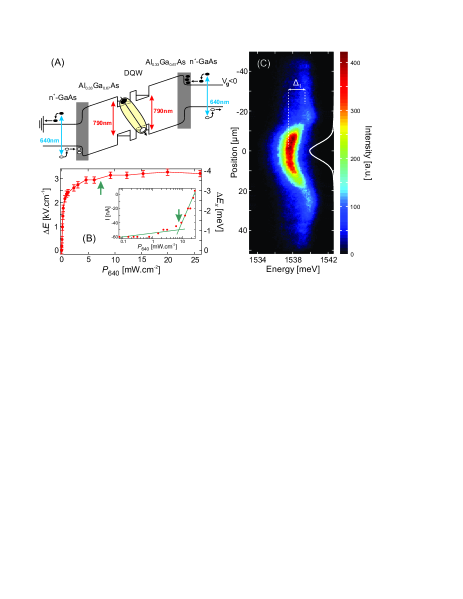
Our optical control relies on a scheme of two laser excitations (Figure 1.A). First, a ”preparation” beam creates an out-of-equilibrium population of charges at the - heterojunctions. This excess of charges modifies the internal electric field. The purpose of the second ”writing” beam is two-fold: first it depletes locally these charges thus producing a lateral potential gradient yielding traps and anti-traps for indirect excitons. In addition, it creates dense gases of indirect excitons inside the DQW, as required to engineer collective quantum phenomena. The ”writing” beam was produced by a laser diode emitting at nm, i.e. at the energy of the DQW direct excitonic transition. Carriers are then photo-created directly inside the DQW where indirect excitons are formed after tunneling towards minimum energy states. The ”preparation” beam wavelength was tuned at 640 nm (from a second laser diode), slightly below the Al0.33Ga0.77As band-gapBosio_1988 . Hence, only a negligible part of the light () is absorbed by the DQW while the largest fraction is absorbed in the -doped GaAs electrodes ( and for the top and back contacts at the right and left hand-side in Fig. 1.A respectivelyMonemar_1976 ). The largest part of the carriers photo-created in the contacts generates a photo-current which increases with the laser intensity, up to nA for the highest excitation power. The other part produces the out-of-equilibrium population of charges electrically transported towards the - heterojunctions. There, potential barriers are formed due to the rectification of potentials between the -GaAs and Al0.33Ga0.77As layersTersoff_1984 . At 350 mK, our bath temperature, the thermal activation is too small ( eV) to overcome these barriersAlloing_2012 . Thus, charges accumulate and then enhance the electric field inside the field-effect devicenote_h .
The resultant internal electric field amplitude () was measured as a function of the power of the ”preparation” beam (see Figure 1.B). was determined from a pump-probe sequence where a ”preparation” pump pulse is followed by a weak excitation probe, from a third laser beam also tuned at 790 nm (see also the Supplementary Informations). The probe pulse creates a dilute gas of indirect excitons in the DQW which acts as a sensitive and non-perturbative probe of . Indeed, the indirect exciton emission energy is governed, in the dilute regime, by the interaction (or Stark effect) between the excitonic dipole ( nm, being the electron charge) and the field, such that . As shown in Fig. 1.B, the electric field amplitude is enhanced by the ”preparation” excitation which manifests that charges accumulate on both sides of the Al0.33Ga0.77As barriers. However, saturates at large pump intensities, as the charge accumulation is too important to be blocked efficiently by the potential barrier at the heterojunctions. This coincides with a steep increase of the photocurrent (see inset in Fig. 1.B).
We observed a strong lateral localization of excess charges over long timescales. This phenomenon is evidenced by the spatially and spectrally resolved emission of indirect excitons, as shown in Fig. 1.C. In these experiments the ”preparation” beam waist was narrowed down to 10 m, while the probe beam waist was much larger, 67 m. The probe beam was turned on 500 ns after the end of the ”preparation” pulse, a delay much longer than the indirect exciton lifetime ( ns, see Supplementary Informations). Then, 20 ns after the end of the probe pulse, the mapping displayed in Fig. 1.C was acquired. Under the ”preparation” beam excitation area, is shifted to lower energies by meV while outside the emission occurs at the unperturbed energy. This indicates that, first, the charge accumulation lasts for several hundreds of nanoseconds, and second, that the carriers lateral diffusion is very slow. Hence, localized excess charges create a confinement potential for indirect excitons. As clearly shown in Fig. 1.C, the emission exhibits a much larger intensity under the region excited by the ”preparation” beam. Indirect excitons created by the probe pulse explore, on the ns timescale, the trapping potential created by the “preparation“ pulse. It has a depth almost two orders of magnitude greater than the thermal activation energy, and as mentioned above, the trap is long-lived, with a lifetime greater than the 500 ns time delay between the “preparation“ and the probe excitations. Therefore, the slow trapping dynamics gives us a unique opportunity to control the excitonic flux, e.g. by optically imprinting a trapping potential and subsequently injecting excitons inside the trap.
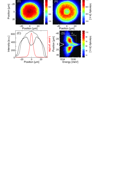
While a weak probe excitation does not perturb the field applied onto the DQW, an intense excitation produced by a ”writing” pulse can significantly affect the spatial profile of the carriers injected by the ”preparation” beam. At the same time the former pulse creates high densities of indirect excitons. This point is illustrated in Figure 2 for an experiment where a tightly focused “writing“ beam (8 m waist) was positioned at the center of a wide ”preparation” laser beam (79 m waist). The time delay between the two pulses is again 500 ns. In Figure 2.A, 20 ns after the ”writing” beam, the spatially resolved emission of indirect excitons exhibits a ring-shaped emission pattern. The inner dark region has a spatial profile reproducing closely the ”writing” beam shape: In this region the photoluminescence signal drops by % compared to a reference situation where no “preparation“ beam is used (see Fig. 2.C). Incidentally, we note for this reference case that the emission has a spatial extension much larger than the writing pulse area itself (see Fig. 2.B): strong repulsive dipolar interactions between indirect excitons induce a large exciton diffusionRemeika_2009 ; Alloing_2011 .
The occurrence of the ring pattern in Fig. 2.A indicates that the central region is now a low field region, from where the excitons are dragged away. Hence, trapped carriers have been depleted from this region by the ”writing” beam. While the mechanism responsible for this depletion is not fully established, we shall underline that the “writing“ beam has a large intensity (1.5 W.cm-2) so that the laser excitation results in a heating restricted to the illuminated region Ivanov_2004 ; Hammack_2009 (see also the Supplementary Informations). Thus, the thermal energy can be sufficient to trigger the diffusion of carriers in the plane of the heterojunctions. To confirm and measure the potential step for indirect excitons in the central region, a third probe beam was used, in the same way as for the experiments shown in Fig. 1.C. The spatial and spectral mapping of the exciton luminescence was measured 20 ns after the probe pulse (Fig. 2D). At the ”writing“ beam position, the exciton energy is larger than in the surrounding, by 2 meV. This shows that the ”writing” beam has introduced a potential gradient, dragging the indirect excitons away from the beam position and thus realizing an anti-trap. Let us note that such a localized potential barrier appears well suited to control the excitonic flux notably in transistor architecturesHigh_2008 ; Grosso_2009 .
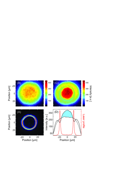
This technique can be easily extended to realize a hollow-trap for indirect excitons, as we show in the following. Such trap consists of a ring-shaped potential barrier confining an excitonic gasGrimm_1998 . To engineer it, we solely shaped the ”writing” beam into a ring. Again we used a sequenced optical control where a spatially wide and uniform “preparation“ pulse is followed by a ring-shaped ”writing“ pulse (see Supplementary Informations). The ring-shaped pattern is shown in Fig. 3.A. It was obtained by using an axicon lens yielding a ring with a 18 m radius and a 3 m thickness. First, we present in Fig. 3.B the spatially resolved emission when the field-effect device is not prepared by the ”preparation” beam. No trace of the ”writing“ beam shape is observed owing to the large diffusion of indirect excitons. On the contrary, when the sample is first prepared by the “preparation“ beam (Fig. 3.C), the emission, 20 ns after the end of the ”writing” pulse, is more intense (same color scale as in Fig 3.B) and localized within the area defined by the ring shape. The writing beam has, at the same time, defined a hollow-trap for excitons and built up a population of indirect excitons which relax rapidly toward the trap center. As shown in Fig. 3.D, this excitation scheme is efficient to create and confine a dense gas of indirect excitons as the photoluminescence increases by as much as 30 % at the center of the trap. From the spectrally resolved photoluminescence emission (see Supplementary Informations), we estimate that the exciton concentration is 5 1010 cm-2 inside the trap. This density lies in the range where quantum statistical signatures are predicted at our very low bath temperatureIvanov_2004 .
Supplementary Informations
I Sample details
We studied a field-effect device which is schematically represented in Figure S1. It consists of a heterostructure embedding a double quantum well (DQW) made of two 8 nm wide GaAs quantum wells separated by a 4 nm Al0.33Ga0.67As barrier. The DQW is placed between two Al0.33Ga0.67As spacers of 200nm thickness. In our experiments, a static potential (Vg) was applied between two n+-GaAs layers (Si doped with cm−3) which serve as gate electrodes. The top and back gates are 105nm and 305nm thick respectively. The back gate is electrically connected with a metallic contact deposited after etching of the sample. In our experiments, this electrode is grounded and electrically isolated from the sample holder by a 800nm undoped GaAs layer incorporating a AlAs/GaAs superlattice. In addition, the top contact consists of a mesa with a 500x500 m2 aperture through which the photoluminescence is collected.
II Experimental Setup
The field-effect device was placed on the Helium 3 insert of a closed cycle Helium 4 cryostat (Heliox-ACV from Oxford Instruments). An aspheric lens with a 0.6 numerical aperture is embedded inside the cryostat in front of the sample and positioned by piezo-electric transducers (ML17 from MechOnics-Ag). We optimized the optical resolution of our microscope by introducing a mechanical coupling between the Helium 3 insert and the part holding the aspheric lens. Thus, the amplitude of mechanical vibrations does not exceed 2 microns (in a frequency range up to 1 kHz) while the sample can be cooled to temperatures as low as 330 mK. In our experiments, the aspheric lens was used to excite the semiconductor sample but also to collect the photoluminescence that was reemitted. The latter was then directed to an imaging spectrograph coupled to an intensified CCD camera (Picostar-UF from La Vision). Thus, we studied the emission of indirect excitons with a 2 ns time resolution, either in real space or including a spectral resolution of 200 eV.
![[Uncaptioned image]](/html/1202.3301/assets/x4.png)
Fig. S1. Schematic representation of the semiconductor sample that we studied at very low temperature (350 mK).
III Electric dipole of indirect excitons
In our experiments, a negative bias (= -1.4 V) was applied to the top gate electrode such that electrons and holes are confined in the bottom and top quantum wells respectively (see Fig. S1). Thus, the ground excitonic transition is of indirect type and indirect excitons exhibit an electric dipole oriented perpendicularly to the plane of the DQW, being the electron charge and r the distance between the electron and hole constituting the exciton. In this geometry, indirect excitons interact strongly with the externally applied electric field E through a dipolar interaction . The amplitude of the electric field in the plane of the DQW is defined by the applied bias and by the thickness of the heterostructure, . It reads . Therefore, the exciton electric dipole moment is deduced by varying the applied voltage, , while monitoring the energy of the photoluminescence emission, . In Figure S2 we present the result of such measurement where we obtained a variation of meV.V-1 which combined with the thickness of our field-effect device ( nm) gives an electric dipole nm for indirect excitons. This value is in good agreement with the characteristic dimension of the DQW where the center of the two quantum wells are separated by 12 nm. The latter distance provides the expected electric dipole moment.
![[Uncaptioned image]](/html/1202.3301/assets/x5.png)
Fig. S2. Variation of the energy of the photoluminescence of indirect excitons, , as a function of the gate voltage, . Measurements were performed at 350 mK and under a weak (5 mW.cm-2) excitation of the DQW at 790 nm to prevent the photo-injection of free carriers. Measurements were realized at 350 mK.
IV Laser induced heating and optical lifetime of indirect excitons
In Figure S3.A-B we show the spectrally and spatially resolved emission of indirect excitons at the end (A) and 4 ns after (B) a 300 ns long ”writing” pulse at 10 W.cm-2. We note during the laser pulse that the emission is weaker in the region which is illuminated compared to outside. Furthermore, once the laser excitation is terminated the signal at the position of the ”writing” beam becomes the most intense (see Fig. S3.C). This behavior is characteristic of indirect excitons and marks the formation and collapse of the so-called inner-ring. It signals a laser induced heating in the region that is illuminated Ivanov_2004 ; Hammack_2009 .
The heating induced by the ”writing” beam is clearly signaled by the photoluminescence dynamics after the laser excitation. Precisely, we show in Fig. S3.D the time resolved emission at the position of the ”writing” beam (red) and outside (blue): at the position of the laser excitation the photoluminescence emission is enhanced by 45 at the end of the ”writing” pulse while the photoluminescence enhancement is much weaker for the region outside of the “writing“ beam. This non-linear response marks the collapse of the inner-ring at the end of the laser excitation. It signals the efficient thermalization of indirect excitons after the ”writing” pulse. Thus, the population of optically active states is enhanced and therefore the photoluminescence emission is sharply increased. Finally, from these measurements we also deduce the optical lifetime of indirect excitons: the photoluminescence obeys a mono-exponential decay after the laser excitation (black line in Fig. S3.D), with a time constant equal to 138(3) ns.
![[Uncaptioned image]](/html/1202.3301/assets/x6.png)
Fig. S3. (A-B): Spatially and spectrally resolved emission of indirect excitons at the end (A) and 4 ns after (B) a ”writing” pulse with 6 m waist and at 10 W.cm-2. (C): Emission profiles at the end of the writing pulse and 4 ns later, solid and dotted lines respectively (the laser profile is shown by the red line). (D): Dynamics of the photoluminescence at the position of the ”writing” pulse (red) and outside (blue). The black line shows the best fit which yields a mono-exponential decay with a time constant equal to 138(3) ns. All measurements were realized at 350 mK.
V Exciton concentration in the hollow-trap
In Figure S4, we present the spatially and spectrally resolved emission of indirect excitons confined in a hollow-trap for the same experimental conditions as for Figure 3.C. We note that the photoluminescence inside the trap is shifted to higher energies, by , than outside the trap where the exciton gas is more dilute. This difference results from the repulsive dipole-dipole interactions between indirect excitons and the energy shift, , gives an estimation of the gas density inside the trap. Indeed, the mean field energy associated to repulsive exciton-exciton interactions may be expressed as , where is a constant factor controlled by the DQW geometry and the correlations between excitons while denotes the exciton density Schindler_08 ; Rapaport_09 . For the experiments displayed in Figure S4 we have 1.3 meV which corresponds to 5 1010 cm-2 Schindler_08 ; Rapaport_09 ; Ben_Tabou_2001 .
![[Uncaptioned image]](/html/1202.3301/assets/x7.png)
Fig. S4. Spatially resolved photoluminescence spectrum along the central axis of the hollow-trap. These measurements were realized in the same experiments as for Fig. 3.C. The white line displays the spatial profile of the “writing“ beam which defines the trap barriers. 1.3 meV is the energy shift of the emission from which the exciton concentration is deduced.
VI Pulse sequences
In our experiments, indirect excitons were optically created by two CW diode lasers (DL-100 from Toptica) at 640nm (“preparation“ beam) and 790nm (“writing“ and probe beams). Both lasers were pulsed with electro-optic (integrated-optical modulator from JenOptic) and acousto-optic modulators (Crystal Technologies Inc.), controlled by a pulse sequencer. Thus, we engineered up to four independent excitation pulses with rising and falling edges of 2ns and 5ns for the electro-optic and acousto-optic switching respectively. The measurements that we report were performed using 4 different pulse sequences which are resumed in Figure S5.
![[Uncaptioned image]](/html/1202.3301/assets/x8.png)
Fig. S5. Blue and red-colored pulses correspond to “preparation“ and “writing“ beams respectively. The green-colored region provides the details of the time window during which real images and spectrally resolved ones were acquired.
References
- (1) I. Bloch, J. Dalibard and W. Zwerger, Rev. Mod. Phys. 80, 885 (2008)
- (2) A.A. High et al., Science 321, 229 (2008)
- (3) V. B. Timofeev, A. V. Gorbunov, Phys. Stat. Sol. (c) 5, 2379 (2008)
- (4) A. A. High et al., Phys. Rev. Lett. 103, 087403 (2009)
- (5) K. Kowalik-Seidl et al., Nano Lett. 12, 326 (2012)
- (6) A. L. Ivanov, J. Phys.: Condens. Matter 16, S3639 (2004)
- (7) J. M. Eisenstein and A. H. Mac Donald, Nature 432, 691 (2004)
- (8) L.V. Butov, J. Phys.: Condens. Matter 19, 295202 (2007)
- (9) D. W. Snoke, Adv. in Condensed Matter Physics (2011); doi:10.1155/2011/938609
- (10) A. F. Croxall et al., Phys. Rev. Lett. 101, 246801 (2008)
- (11) J. A. Seamons et al., Phys. Rev. Lett. 102, 026804 (2009)
- (12) Chen G. et al., Phys. Rev. B 74, 045309 (2006)
- (13) A. Gaertner et al., Phys. Rev. B 76, 085304 (2007)
- (14) E. Wertz et al., Nature Phys. 6, 860 (2010)
- (15) A. Amo et al., Phys. Rev. B 82, 081301(R) (2010)
- (16) A.T. Hammack et al., Phys. Rev. Lett. 96, 227402 (2006)
- (17) C. Bosio et al., Phys. Rev. B 38, 3263 (1988)
- (18) B. Monemar, K. K. Shih and G. D. Pettit, J. Appl. Phys. 47, 2604 (1976)
- (19) J. Tersoff, Phys. Rev. B 30, 4874(R) (1984)
- (20) M. Alloing et al., arXiv:1202.1985
- (21) the injection of holes results in a deficit of electrons increasing the potential of the -GaAs electrode on the left hand-side in Fig. 1.A
- (22) M. Remeika et al., Phys. Rev. Lett. 102, 186803 (2009)
- (23) M. Alloing et al., EuroPhys. Lett. 93, 17007 (2011)
- (24) A.T. Hammack et al., Phys. Rev. B 80, 155331 (2009)
- (25) A. G. Winbow et al., Phys. Rev. Lett. 106, 196806 (2011)
- (26) I. Manek, Y. B. Ovchinnikov, R. Grimm, Optics. Comm. 147, 67 (1998)
- (27) C. Schindler and R. Zimmermann, Phys. Rev. B 78, 045313 (2008)
- (28) B. Laikhtman. and R. Rapaport, Phys. Rev. B 80, 195313 (2009)
- (29) S. Ben-Tabou de-Leon, B. Laikhtman, Phys. Rev. B 63, 125306 (2001)