Topological p-n Junction
Abstract
We consider a junction between surface -type and surface -type on an ideal topological insulator in which carrier type and density in two adjacent regions are locally controlled by composition graded doping or electrical gating. Such junction setting on topological insulators are fundamental for possible device application. A single gapless chiral edge state localized along the junction interface appears in the presence of an external magnetic field, and it can be probed by scanning tunneling microscopy and transport measurements. We propose to realize this topological p-n junction in (Bi1-xSbx)2Te3, which has insulating bulk properties and a tunable surface state across the Dirac cone.
pacs:
73.20.-r 73.43.Cd 68.37.Ef 73.40.LqTopological insulators are new states of quantum matter with a full insulating gap in the bulk and gapless edge or surface states interesting for condensed matter physics Qi and Zhang (2010); Moore (2010); Hasan and Kane (2010); Qi and Zhang (2011). The surface states of a three-dimensional (3D) topological insulator are comprised of an odd number of massless Dirac cones with spin helical structure in the momentum space which are protected by time-reversal symmetry. Such spin-helical metallic surface states are expected to host a wide range of exotic quantum phenomena such as Majorana fermions Fu and Kane (2008), image magnetic monopole Qi et al. (2009) and topological magneto-electric effect Qi et al. (2008). The single Dirac cone on the Bi2X3 (X = Se and Te) surface Zhang et al. (2009); Xia et al. (2009); Chen et al. (2009) can be viewed as one quarter of graphene Novoselov et al. (2005), and it is predicted to exhibit half-Integer quantum Hall effect Qi et al. (2008), which is a unique property of a time-reversal symmetry-breaking surface and is determined by the bulk topology. Extensive efforts such as chemical doping and electric gating have been made to achieve the purely conducting surface in transport on topological insulators Hsieh et al. (2009); Checkelsky et al. (2009); Analytis et al. (2010); Qu et al. (2010); Chen et al. (2010); Checkelsky et al. (2011); Taskin et al. (2011); Ren et al. (2011), however, they are hindered by intrinsic defects in the materials where Bi2X3 is the significant bulk conduction.
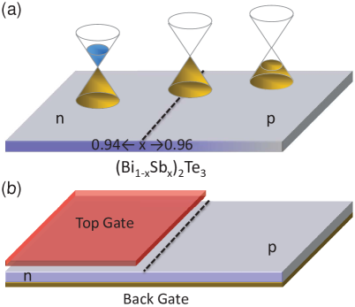
Recently, three experimental groups have successfully engineered the band structure of topological insulators by molecular beam epitaxy growth of (Bi1-xSbx)2Te3 Zhang et al. (2011); Kong et al. (2011) ternary compounds and tetradymite Bi2-xSbxTe3-ySey Arakane et al. (2012). By tuning the ratio of bismuth to antimony, they can get ideal topological insulators with truly insulating bulk and tunable surface state across the Dirac cone (p- to n-type) that behave like 1/4 of graphene. By composition graded doping one may form a p-n junction (PNJ) on a topological insulator surface [see Fig. 1], which is similar to graphene PNJ Williams et al. (2007); Huard et al. (2007). The properties in such a junction setting of topological insulators are not yet known Wray et al. . On the other hand, graphene PNJs are not only promising for transistor, but also are predicted to host novel phenomena reflecting the massless Dirac character of carriers such as Klein tunneling Katsnelson et al. (2006) and Veselago lensing Cheianov et al. (2007). Therefore, it is important and straightforward to study the physics and relevant applications of PNJ on a topological insulator surface in analogy of graphene junction. The topological insulator surface junction is also different from the graphene junction for it only consists of a single Dirac cone. If a magnetic field is applied perpendicular to the surface junction, the different types of the carriers would give rise to a quantized Hall conductance in the n and p regions, respectively, so that a single chiral edge state arises along the p-n interface. In the following, we will refer to such PNJ on a topological insulator surface as ‘topological p-n junction’. The gapless chiral edge mode localized at the PNJ can be controlled by gating and magnetic field, which may be probed through scanning tunneling microscopy (STM) and transport measurements.
We propose two methods to fabricate the topological p-n junction. One is composition graded doping, the other is electrostatic gating. The compound (Bi1-xSbx)2Te3 with (0.96) is an ideal topological insulator with surface n (p)-doping, where the surface Dirac cone is in the insulating bulk gap and the Fermi level stays slightly above (below) the Dirac cone Zhang et al. (2011). In analogy to the growth method of PNJ in p-GaAs/n-AlxGa1-xAs, one can fabricate the junction between p-type and n-type topological insulators by composition graded doping from to to achieve spatially variable Dirac cone structures [Fig. 1(a)]. While in electrostatic gating, one can use the global back gate to control the position of surface Dirac cone in the bulk gap, combined with the local top gate to control density and carrier type locally [Fig. 1(b)]. This will result in device configurations with adjacent n-type and p-type regions on top surface sta , separated by an electrically tunable PNJ, very similar to graphene PNJ Williams et al. (2007). Different from the gating in graphene PNJ, here the capability of the top gate to control the carrier type and density is limited, therefore it is better to start from (Bi1-xSbx)2Te3 with rather than Bi2Te3 or Sb2Te3. The Fermi velocity of Dirac electron in the p and n regions of such topological p-n junction are almost the same Zhang et al. (2011). The thickness of depletion layer of the junction at zero bias can be estimated through Poisson equation , where is the dielectric constant, is the electric potential, is the carrier density. With the condition that there are no free carriers in the depletion area, one can get the relation between thickness of depletion layer and potential barrier , . () is the surface electron (hole) density, is the depth of surface state inside the sample. With nm, , meV, cm-2, the thickness of the topological p-n junction is estimated to be nm.
The effective model Zhang et al. (2009); Liu et al. (2010) describing the massless 2D Dirac fermion of a topological p-n junction reads
| (1) |
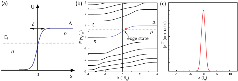
where is the Fermi velocity, are Pauli matrices that act on the electron spin degrees of freedom, is the canonical momentum operator on the surface (- plane), we set , is the electrostatic potential step at the p-n interface, which can be modeled as , and is just the Fermi energy difference between the - and -region [see Fig. 2(a)]. On such junction setting, due to the suppressed backscattering on the topological insulator surface, the interference between the incident and reflected waves will results in a standing wave pattern on the surface which decays faster than conventional two-dimensional (2D) electron gas, and has been observed by STM experimentally Wang et al. (2011).
More interestingly, when a perpendicular magnetic field is applied to the junction, a gapless chiral edge state may appear along the interface in the quantum Hall regime. The basic picture of the formation of chiral edge state along the PNJ is easily visualized as skipping orbital semiclassically, the change in sign of charge carriers across the PNJ produces a change in the direction of the Lorentz force, causing classical trajectories to curve back towards the interface from both sides. The orbital effect of magnetic field can be obtained by Peierls substitution in Eq. (1), where is the vector potential. Here we choose the Landau gauge, thus is parallel to the PNJ and vanishes at the interface, and the canonical momentum along -axis is a good quantum number. The energy spectrum for the PNJ is plotted in Fig. 2(b) with (the magnetic length nm at T). The Fermi level intersects with only one chiral channel of mixed electron-hole character with linear dispersion (blue curve), where the electronlike channel is from the n region and holelike channel is from the p region, both of them are from the non-degenerate zero mode of Landau levels (LLs), and contribute to Hall conductance. The density of the chiral edge state is shown in Fig. 2(c), which is indeed the edge mode confined along the PNJ. The scale of such chiral edge state is about nm, which is smooth on the scale of . To see the chiral edge state more clearly we consider a abrupt potential step, and in order to simplify the notation, we measure energies in units of and lengths in units of . Eigenstates of Eq. (1) with magnetic field that decay for have the form Akhmerov and Beenakker (2007)
| (2) | |||||
| (3) | |||||
| (4) |
here is the Hermite function. The dispersion relation between energy and momentum follows by substitution of state (2) into the boundary condition , and particle current conservation . Thus we obtain
| (5) |
The numerical solution of the Eq. (5) is qualitatively similar to Fig. 2(c). For , the LLs energy in the n region are at , which is ; while for , the energy is , which is , and the velocity vanishes. Those flat bands at finite in Fig. 2(c) are LLs in the and regions. The chiral edge state does not exist if the potential barrier is too high, in that case the p and n regions are independent, and the edge channels from both sides can not couple to each other due to energy mismatch. From Eq. (5), the chiral edge state with around exists only when and , which gives the criterion is
| (6) |
where the right part is just the energy difference between the second LL and zero mode. This reflects that increasing the electric field across the junction via gate voltages will destabilize the edge modes. With meV, the magnetic field must greater than T in order for such edge state exists.
We now propose a practical way to detect such chiral edge state [see Fig. 3(a)]. The state localized at the junction on a topological insulator surface can be imaged by STM. By applying a magnetic field, the LLs structure of surface states is formed and has already been observed by STM Cheng et al. (2010); Hanaguri et al. (2010). Discrete LLs appear as a series of peaks in the differential conductance spectrum (), and the dependence of the LLs on the magnetic field shows that the energy of the LLs is proportional to , where is the LL index. The energy of zero mode in the p and n regions can be measured, between which there are no states in either region as shown in Fig. 3(b). Then by moving the STM tip to the PNJ area, one should observe a peak in the spectrum with energy between zero mode in the p and n regions, and this should be the manifestation of the chiral edge mode. Moreover, the formation of the chiral edge mode takes place at a , therefore such peak will disappear in the spectrum when decreasing the magnetic field.
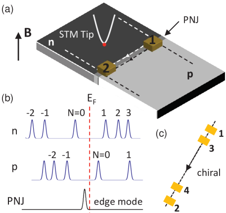
In addition to the above surface-sensitive technique, one can employ transport measurements. Instead of measuring the Hall conductance, we can directly measure the longitudinal resistance along the PNJ. In conventional junction, there is no conducting channel along PNJ. However, in the quantum Hall regime, the single chiral edge mode along topological p-n junction will contribute to transport. As shown in Fig. 3(c), is measured along the PNJ, with current source at 1, ground at 2, and voltage measured between 3 and 4, we will get the longitudinal resistance contributed from the chiral edge channel. Backscattering is forbidden along this channel, therefore by reversing the current flow at 1 and 2, will approach infinity. Besides this, when the magnetic field is smaller than the critial value , such chiral edge channel will disappear, and we will get zero conductance.
In summary, we propose to use composition graded doping and electric gating in topological insulator alloys (Bi1-xSbx)2Te3 to fabricate the topological p-n junction, where a single 2D Dirac cone junction on a topological insulator surface may be achieved. A single gapless chiral edge state localized along the p-n interface appears in the presence of an external magnetic field, which can be controlled by the gating and magnetic field. The edge mode can be imaged by STM as well as transport measurements. The topological p-n devices would lead to novel designs for opto-electronics applications.
We are grateful to X. L. Qi and Yayu Wang for insightful discussion. This work is supported by the Department of Energy, Office of Basic Energy Sciences, Division of Materials Sciences and Engineering, under contract DE-AC02-76SF00515. J. Wang is partly supported by the Program of Basic Research Development of China Grant No. 2011CB921901.
References
- Qi and Zhang (2010) X. L. Qi and S. C. Zhang, Phys. Today 63, No. 1, 33 (2010).
- Moore (2010) J. E. Moore, Nature 464, 194 (2010).
- Hasan and Kane (2010) M. Z. Hasan and C. L. Kane, Rev. Mod. Phys. 82, 3045 (2010).
- Qi and Zhang (2011) X. L. Qi and S. C. Zhang, Rev. Mod. Phys. 83, 1057 (2011).
- Fu and Kane (2008) L. Fu and C. L. Kane, Phys. Rev. Lett. 100, 096407 (2008).
- Qi et al. (2009) X. L. Qi, R. Li, J. Zang, and S. C. Zhang, Science 323, 1184 (2009).
- Qi et al. (2008) X. L. Qi, T. L. Hughes, and S. C. Zhang, Phys. Rev. B 78, 195424 (2008).
- Zhang et al. (2009) H. Zhang, C.-X. Liu, X.-L. Qi, X. Dai, Z. Fang, and S.-C. Zhang, Nature Phys. 5, 438 (2009).
- Xia et al. (2009) Y. Xia, D. Qian, D. Hsieh, L. Wray, A. Pal, H. Lin, A. Bansil, D. Grauer, Y. S. Hor, R. J. Cava, and M. Z. Hasan, Nature Phys. 5, 398 (2009).
- Chen et al. (2009) Y. L. Chen, J. G. Analytis, J.-H. Chu, Z. K. Liu, S.-K. Mo, X. L. Qi, H. J. Zhang, D. H. Lu, X. Dai, Z. Fang, S. C. Zhang, I. R. Fisher, Z. Hussain, and Z.-X. Shen, Science 325, 178 (2009).
- Novoselov et al. (2005) K. S. Novoselov, A. K. Geim, S. V. Morozov, D. Jiang, M. I. Katsnelson, I. V. Grigorieva, S. V. Dubonos, and A. A. Firsov, Nature (London) 438, 197 (2005).
- Hsieh et al. (2009) D. Hsieh, Y. Xia, D. Qian, L. Wray, J. H. Dil, F. Meier, J. Osterwalder, L. Patthey, J. G. Checkelsky, N. P. Ong, A. V. Fedorov, H. Lin, A. Bansil, D. Grauer, Y. S. Hor, R. J. Cava, and M. Z. Hasan, Nature 460, 1101 (2009).
- Checkelsky et al. (2009) J. G. Checkelsky, Y. S. Hor, M.-H. Liu, D.-X. Qu, R. J. Cava, and N. P. Ong, Phys. Rev. Lett. 103, 246601 (2009).
- Analytis et al. (2010) J. G. Analytis, R. D. McDonald, S. C. Riggs, J.-H. Chu, G. S. Boebinger, and I. R. Fisher, Nature Phys. 6, 960 (2010).
- Qu et al. (2010) D. X. Qu, Y. S. Hor, J. Xiong, R. J. Cava, and N. P. Ong, Science 329, 821 (2010).
- Chen et al. (2010) J. Chen, H. J. Qin, F. Yang, J. Liu, T. Guan, F. M. Qu, G. H. Zhang, J. R. Shi, X. C. Xie, C. L. Yang, K. H. Wu, Y. Q. Li, and L. Lu, Phys. Rev. Lett. 105, 176602 (2010).
- Checkelsky et al. (2011) J. G. Checkelsky, Y. S. Hor, R. J. Cava, and N. P. Ong, Phys. Rev. Lett. 106, 196801 (2011).
- Taskin et al. (2011) A. A. Taskin, Z. Ren, S. Sasaki, K. Segawa, and Y. Ando, Phys. Rev. Lett. 107, 016801 (2011).
- Ren et al. (2011) Z. Ren, A. A. Taskin, S. Sasaki, K. Segawa, and Y. Ando, Phys. Rev. B 84, 165311 (2011).
- Zhang et al. (2011) J. Zhang, C.-Z. Chang, Z. Zhang, J. Wen, X. Feng, K. Li, M. Liu, K. He, L. Wang, X. Chen, Q.-K. Xue, X. Ma, and Y. Wang, Nature Comms. 2, 574 (2011).
- Kong et al. (2011) D. Kong, Y. Chen, J. J. Cha, Q. Zhang, J. G. Analytis, K. Lai, Z. Liu, S. S. Hong, K. J. Koski, S.-K. Mo, Z. Hussain, I. R. Fisher, Z.-X. Shen, and Y. Cui, Nature Nano. 6, 705 (2011).
- Arakane et al. (2012) T. Arakane, T. Sato, S. Souma, K. Kosaka, K. Nakayama, M. Komatsu, T. Takahashi, Z. Ren, K. Segawa, and Y. Ando, Nature Comms. 3, 636 (2012).
- Williams et al. (2007) J. R. Williams, L. DiCarlo, and C. M. Marcus, Science 317, 638 (2007).
- Huard et al. (2007) B. Huard, J. A. Sulpizio, N. Stander, K. Todd, B. Yang, and D. Goldhaber-Gordon, Phys. Rev. Lett. 98, 236803 (2007).
- (25) L. A. Wray, S. Xu, M. Neupane, D. Hsieh, D. Qian, A. V. Fedorov, H. Lin, S. Basak, A. Bansil, Y. S. Hor, R. J. Cava, and M. Z. Hasan, arxiv: cond-mat/1105.4794 (2011).
- Katsnelson et al. (2006) M. I. Katsnelson, K. S. Novoselov, and A. K. Geim, Nature Phys. 2, 620 (2006).
- Cheianov et al. (2007) V. V. Cheianov, V. Fal’ko, and B. L. Altshuler, Science 315, 1252 (2007).
- (28) In general, the top surface and bottom surface are not exactly the same due to the substrate, therefore a PNJ could be realized only on top surface by doping and gating, while the bottom surface is just p or n doped.
- Liu et al. (2010) C.-X. Liu, X.-L. Qi, H. Zhang, X. Dai, Z. Fang, and S.-C. Zhang, Phys. Rev. B 82, 045122 (2010).
- Wang et al. (2011) J. Wang, W. Li, P. Cheng, C. Song, T. Zhang, P. Deng, X. Chen, X. Ma, K. He, J.-F. Jia, Q.-K. Xue, and B.-F. Zhu, Phys. Rev. B 84, 235447 (2011).
- Akhmerov and Beenakker (2007) A. R. Akhmerov and C. W. J. Beenakker, Phys. Rev. Lett. 98, 157003 (2007).
- Cheng et al. (2010) P. Cheng, C. Song, T. Zhang, Y. Zhang, Y. Wang, J.-F. Jia, J. Wang, Y. Wang, B.-F. Zhu, X. Chen, X. Ma, K. He, L. Wang, X. Dai, Z. Fang, X. Xie, X.-L. Qi, C.-X. Liu, S.-C. Zhang, and Q.-K. Xue, Phys. Rev. Lett. 105, 076801 (2010).
- Hanaguri et al. (2010) T. Hanaguri, K. Igarashi, M. Kawamura, H. Takagi, and T. Sasagawa, Phys. Rev. B 82, 081305 (2010).