Simulation of spin-polarized scanning tunneling spectroscopy on complex magnetic surfaces: Case of a Cr monolayer on Ag(111)
Abstract
We propose a computationally efficient atom-superposition-based method for simulating spin-polarized scanning tunneling spectroscopy (SP-STS) on complex magnetic surfaces based on the sample and tip electronic structures obtained from first principles. We go beyond the commonly used local density of states (LDOS) approximation for the differential conductance, dI/dV. The capabilities of our approach are illustrated for a Cr monolayer on a Ag(111) surface in a noncollinear magnetic state. We find evidence that the simulated tunneling spectra and magnetic asymmetries are sensitive to the tip electronic structure, and we analyze the contributing terms. Related to SP-STS experiments, we show a way to simulate two-dimensional differential conductance maps and qualitatively correct effective spin polarization maps on a constant current contour above a magnetic surface.
pacs:
72.25.Ba, 68.37.Ef, 71.15.-m, 73.22.-fI Introduction
The scanning tunneling microscope (STM) and its spectroscopic mode (STS) proved to be extremely useful for studying local physical and chemical phenomena on surfaces since the invention of the STM 30 years ago Binnig et al. (1982, 1982). The progress of experimental techniques in the last two decades was remarkable, thus, more sophisticated theoretical models and simulation tools are needed to explain all relevant details of electron tunneling transport measurements Hofer et al. (2003); Hofer (2003). STS theory and applications are recently focused on extracting surface local electronic properties from experimental differential conductance () data Ukraintsev (1996); Koslowski et al. (2007); Passoni et al. (2009); Ziegler et al. (2009); Koslowski et al. (2009). The role of the tip electronic structure has been identified to be crucial on the tunneling spectra, see e.g. Refs. Passoni et al. (2009); Kwapiński and Jałochowski (2010), and a theoretical method has been proposed to separate the tip and sample contributions to STS Hofer and Garcia-Lekue (2005).
An emerging research field in surface science is the investigation of magnetism at the nanoscale and atomic scale with the aim of achieving ultrahigh information density for data storage purposes Plumer et al. (2001); Weiss et al. (2005). Spin-polarized scanning tunneling microscopy (SP-STM) Bode (2003) is admittedly an important tool for studying magnetism on surfaces. Recent experimental advances using this technique allow the investigation of complex magnetic structures (frustrated antiferromagnets, spin spirals, skyrmion lattices, etc.) Wiesendanger (2009); Wulfhekel and Gao (2010); Serrate et al. (2010); Heinze et al. (2011). Spin-polarized scanning tunneling spectroscopy (SP-STS) has recently been used to find inversion of spin polarization above magnetic adatoms Yayon et al. (2007); Heinrich et al. (2009); Zhou et al. (2010), and the effect has been explained theoretically Ferriani et al. (2010). Furthermore, SP-STS is useful to study atomic magnetism Wiebe et al. (2011), many-body effects on substrate-supported adatoms Néel et al. (2010), or magnetic interactions between adatoms Ternes et al. (2009) as well. The effect of differently magnetized surface regions on SP-STS has also been reported Schouteden et al. (2008); Heinrich et al. (2010), and the role of tip effects on SP-STS Rodary et al. (2009); Palotás et al. (2011) and on achieving giant magnetic contrast Hofer et al. (2008) have also been highlighted.
Our work is concerned with the presentation of an efficient simulation method for SP-STS based on first principles electronic structure data. We extend our atom-superposition-based method Palotás et al. (2011, 2011) in the spin-polarized Tersoff-Hamann framework Wortmann et al. (2001) for simulating SP-STS by including the bias dependent background and tip-derivative terms into the calculated differential conductance following Passoni et al. Passoni et al. (2009). The method is computationally cheap and it can be applied using results of any ab initio electronic structure code. The main advance of our tunneling model is the inclusion of the tip electronic structure, which is neglected in Refs. Wortmann et al. (2001); Heinze (2006), and it is only taken into account in a model way in Ref. Passoni et al. (2009). Our method, based on first principles calculation of the tip electronic structure, enables to study tip effects on the SP-STS spectra. Taking a prototype frustrated hexagonal antiferromagnetic system, a Cr monolayer on Ag(111) in a noncollinear magnetic Néel state, we simulate differential conductance tunneling spectra and magnetic asymmetries to illustrate the applicability of our method, and we analyze the contributing terms. Note that a three-dimensional (3D) approach to STS has been presented recently, that is applicable to nonmagnetic systems only, and it takes into account the symmetry of the tip states but not the electronic structure of the tip apex Donati et al. (2011). Our model is also a 3D approach in the sense that we sum up contributions from individual transitions between the tip apex atom and each of the surface atoms assuming the one-dimensional (1D) Wentzel-Kramers-Brillouin (WKB) approximation for electron tunneling processes in all these transitions, thus we call it a 3D WKB approach.
The paper is organized as follows: The atom-superposition theoretical model of SP-STS is presented in section II. As an application, we investigate the surface of one monolayer (ML) Cr on Ag(111) in section III. We simulate differential conductance tunneling spectra and magnetic asymmetries with two tip models, and we analyze the contributing terms to . Moreover, we show simulation results of bias dependent two-dimensional (2D) differential conductance and qualitatively correct effective spin polarization maps following a constant current contour above the surface, corresponding to a standard experimental setup. Our conclusions are found in section IV. Finally, in appendix A, we report the 1D WKB theory of STS, and give alternative expressions for the .
II Theoretical model of atom-superposition SP-STS
The 1D WKB theory for nonmagnetic STS is a well established approach Ukraintsev (1996); Passoni and Bottani (2007), see appendix A. Here, we extend it to spin-polarized systems, and adapt it to an atom superposition framework, which enables a computationally inexpensive calculation of tunneling properties based on first principles electronic structure data.
In magnetic STM junctions, the total tunneling current can be decomposed into non-spinpolarized (TOPO) and spin-polarized (MAGN) parts Wortmann et al. (2001); Yang et al. (2002); Smith et al. (2004); Heinze (2006),
| (1) |
Following the spin-polarized Tersoff-Hamann model Wortmann et al. (2001) and its adaptation to the atom superposition framework Heinze (2006); Palotás et al. (2011), the magnetic contribution to the simple expression of the differential conductance at a given energy is proportional to the scalar product of the tip and sample magnetic density of states (DOS) vectors, and , respectively,
| (2) |
Thus, the spin-polarized parts of can similarly be calculated within the 1D WKB approximation as reported in appendix A, just replacing by .
We formulate the tunneling current, the differential conductance and their TOPO and MAGN parts within the atom superposition framework following Ref. Palotás et al. (2011). Here, we assume that electrons tunnel through one tip apex atom, and we sum up contributions from individual transitions between this apex atom and each of the surface atoms assuming the 1D WKB approximation for electron tunneling processes in all these transitions. The tunneling current at the tip position and at bias voltage is given by
| (3) |
where the TOPO and MAGN terms are formally given as
| (4) | |||||
| (5) |
The integrands are the so-called virtual differential conductances,
| (6) | |||||
| (7) |
Here, is the elementary charge, the Planck constant, and and the Fermi energies of the tip and the sample surface, respectively. ensures that the is correctly measured in the units of . has been chosen to 1 eV, but its actual value has to be determined comparing simulation results to experiments. The sum over corresponds to the atomic superposition and has to be carried out, in principle, over all surface atoms. Convergence tests, however, showed that including a relatively small number of atoms in the sum provides converged values Palotás et al. (2011). The tip and sample electronic structures are included into this model via projected DOS (PDOS) onto the atoms, i.e. and denote projected charge DOS onto the tip apex and the th surface atom, respectively, while and are projected magnetization DOS vectors onto the corresponding atomic spheres. They can be obtained from collinear or noncollinear electronic structure calculations Palotás et al. (2011). In the present work we determine the noncollinear PDOS for the sample surface and we use a collinear PDOS for a model CrFe tip Ferriani et al. (2010).
The transmission probability for electrons tunneling between states of atom on the surface and the tip apex is of the simple form,
| (8) |
This corresponds to a spherical exponential decay of the electron wavefunctions. Here, is the distance between the tip apex and the surface atom labeled by with position vector . Assuming an effective rectangular potential barrier between the tip apex and each surface atom, the vacuum decay can be written as
| (9) |
where the electron’s mass is , is the reduced Planck constant, and and are the average electron workfunction of the sample surface and the local electron workfunction of the tip apex, respectively. The method of determining the electron workfunctions is reported in Ref. Palotás et al. (2011). is treated within the independent orbital approximation Tersoff and Hamann (1983, 1985); Heinze (2006), which means that the same spherical decay is used for all type of orbitals. The interpretation of our simulation results with quantitative reliability compared to experiments has to be taken with care due to this approximation. However, extension of our model to take into account orbital dependent vacuum decay following Chen’s work Chen (1990) is planned in the future, which is relevant for a more advanced description of tunneling between directional orbitals.
Moreover, in our model, the electron charge and magnetization local density of states above the sample surface in the vacuum, and , respectively, are approximated by the following expressions:
| (10) | |||
| (11) |
with
| (12) |
Note that the exact LDOS can be obtained by explicitly calculating the decay of the electron states into the vacuum taking their orbital symmetry into account as well, not via such a simple 3D WKB model. Our approach, however, has computational advantages as discussed in Ref. Palotás et al. (2011).
Similarly to the tunneling current, the physical differential conductance can be decomposed into non-spinpolarized (TOPO) and spin-polarized (MAGN) parts and it can be written at the tip position and at bias voltage as
| (13) |
where the contributions are given as [see Eq.(41) in appendix A]
| (14) | |||||
| (15) |
Here, and are the background and tip-derivative terms, respectively, see appendix A. The background term, which contains the bias-derivative of the transmission function, is usually taken into account in recent STS theories Passoni and Bottani (2007); Passoni et al. (2009); Donati et al. (2011), while the tip-derivative term containing the energy derivative of the tip DOS is rarely considered in the recent literature. Obviously, the total differential conductance can also be written in the same structure,
| (16) |
with
| (17) | |||||
| (18) | |||||
| (19) |
In order to calculate the background term, we need the bias-derivative of the transmission function. Using Eq.(8) and the given form of the vacuum decay in Eq.(9), we obtain
| (20) |
Considering this, and the corresponding components in the 1D WKB model, Eqs. (43) and (44) in appendix A, the background and the tip-derivative contributions can be written as
Thus, we formulated all components of the differential conductance in spin-polarized tunnel junctions within the atom superposition framework using first principles electronic structure of the sample and the tip. Note that all expressions in Eq.(A) in appendix A can similarly be calculated within our 3D WKB approach.
and can be calculated at grid points of a three-dimensional (3D) fine grid in a finite box above the surface. The recipe for simulating SP-STM images based on the 3D current map is given in Ref. Palotás et al. (2011). Here, we focus on the simulation of spectra. From the 3D differential conductance map, data can be extracted that are directly comparable to experiments. For example, a single point spectrum corresponds to a fixed tip position, and two-dimensional (2D) spectra can also be obtained, where the image resolution is determined by the density of grid points. There are usually two ways to define a 2D differential conductance map Wiesendanger (2009). The first method fixes the tip height at and scans the surface, . The second option measures on a constant current contour, , which is the widely used method in experiments. Simulation of this can be done in two steps: First, we calculate the 3D current map with the given bias voltage , and at the second step we determine the height profile of a constant current contour, , using logarithmic interpolation Palotás et al. (2011). and are the tunneling parameters, and they stabilize the tip position at the height of above the sample surface point. The 2D differential conductance map on the constant current contour is then given by , where the -dependence is obtained by sweeping the bias voltage range using a lock-in technique in experiments Wiesendanger (2009). Recently, experimental efforts have been made to extract the TOPO component of the tunneling current Ding et al. (2003), and measure spectroscopic data on such constant current contours, i.e. at Tange et al. (2010). According to Ref. Wiesendanger (2009), a constant tunneling transmission enables an easier interpretation of measured 2D spectroscopic data. We believe that a constant TOPO current contour is closer to this constant tunneling transmission criterion than a constant TOTAL current contour due to the appearance of spin dependent effects in the latter one. On the other hand, the calculation of any current contour is simple within our 3D WKB approach Palotás et al. (2011). Since the experimental method is not routinely available at the moment, we restrict ourselves to consider the contours when calculating the 2D differential conductance maps, and we will show examples in the next section.
By simulating differential conductance spectra above a magnetic surface with parallel (P) and antiparallel (AP) tip magnetization directions with respect to a pre-defined direction (usually the magnetization direction of a chosen surface atom is taken), the so-called magnetic asymmetry can be defined Zhou et al. (2010). In our case this quantity can be calculated at all considered positions of the tip apex atom, i.e. at all grid points within our finite box above the surface:
| (25) |
From this, the magnetic asymmetry can similarly be calculated on appropriate constant current contours as described in the previous paragraph. Using Eq.(13), and the fact that the magnetic contribution for the AP tip magnetization direction equals , since the tip magnetization PDOS vector changes sign at all energies compared to the P tip magnetization direction, the differential conductances take the following form:
| (26) |
Thus, the magnetic asymmetry can be expressed as the fraction of the MAGN and TOPO differential conductances from Eqs. (14) and (15) as
This is the correct magnetic asymmetry expression based on the physical differential conductances that can be obtained from experiments. However, a magnetic asymmetry can similarly be defined taking the virtual differential conductances from Eqs. (6) and (7):
| (28) |
This is an important quantity since it is related to the vacuum spin polarization of the sample in a simple way Zhou et al. (2010):
| (29) |
i.e., is the effective spin polarization (ESP): the scalar product of the tip spin polarization vector at its Fermi level, , and the vacuum spin polarization vector of the sample at , above the sample Fermi level, . Following above, it is clear that the determination of the sample spin polarization from experimentally measured spectra is not straightforward since the experimentally accessible magnetic asymmetry according to the equivalent expressions Eq.(25) and Eq.(II) contains the background and tip-derivative terms as well. On the other hand, we can easily calculate ESP within our method. There are even more possibilities to define magnetic asymmetries, by adding the background terms in Eqs. (II) and (II), or the tip-derivative terms in Eqs. (II) and (II) to the corresponding virtual differential conductance and then performing the division:
| (30) | |||
| (31) |
As is one component of according to Eq.(16), we will compare them and also the magnetic asymmetry expressions in Eqs. (II)-(31), in order to estimate the error one makes when neglecting the background and tip-related components of for a given combination of a complex magnetic surface and a magnetic tip. On the other hand, we will calculate qualitatively correct bias dependent 2D effective spin polarization maps following a constant current contour.
It has to be noted that the presented method can also be applied to study nonmagnetic systems, where all magnetic contributions equal zero and the corresponding topographic STS spectra can be simulated. Of course, in this case, the magnetic asymmetry is zero.
III Results and Discussion
In order to demonstrate the reliability and capabilities of our model for simulating SP-STS on complex magnetic surfaces, we consider a sample surface with noncollinear magnetic order. One ML Cr on Ag(111) is a prototype of frustrated hexagonal antiferromagnets Heinze (2006). Due to the geometrical frustration of the antiferromagnetic exchange interactions between Cr spin moments, its magnetic ground state is a noncollinear Néel state Wortmann et al. (2001). In the presence of spin-orbit coupling, two types of Néel states with opposite chiralities can form, and one of them is energetically favored Palotás et al. (2011).
We performed geometry relaxation and electronic structure calculations based on Density Functional Theory (DFT) within the Generalized Gradient Approximation (GGA) implemented in the Vienna Ab-initio Simulation Package (VASP) Kresse and Furthmüller (1996a, b); Hafner (2008). A plane wave basis set for electronic wavefunction expansion together with the projector augmented wave (PAW) method Kresse and Joubert (1999) has been applied, while the exchange-correlation functional is parametrized according to Perdew and Wang (PW91) Perdew and Wang (1992). For calculating the fully noncollinear electronic structure we used the VASP code as well Hobbs et al. (2000); Hobbs and Hafner (2000), with spin-orbit coupling considered.
We model the Cr/Ag(111) system by a slab of a five-layer Ag substrate and one monolayer Cr film on each side, where the surface Cr layers and the first Ag layers underneath have been fully relaxed. A separating vacuum region of 14.6 width in the surface normal () direction has been set up between neighboring supercell slabs. The average electron workfunction above the surface is eV. We used an Monkhorst-Pack (MP) Monkhorst and Pack (1976) k-point grid for calculating the projected electron DOS (PDOS) onto the surface Cr atoms in our () magnetic surface unit cell Palotás et al. (2011).
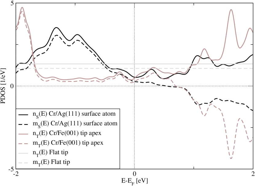
The energy dependent charge and magnetization PDOS, and , respectively, are shown in Figure 1. We obtained these quantities from noncollinear calculations. The spin quantization axis of each surface Cr atom is chosen to be parallel to their magnetic moment direction, and is the projection of the magnetization PDOS vector to this direction. Except the spin quantization axes of the three different Cr atoms in the magnetic surface unit cell, their electronic structure is the same. We can interpret the results in terms of the commonly used spin up (, majority) and spin down (, minority) channels with respect to the atomic spin quantization axis, where , and . It is seen that the majority spin PDOS dominates over the minority spin PDOS below eV, while above eV. This implies a spin polarization reversal at this particular energy Palotás et al. (2011).
In our model, the vacuum local density of states (LDOS) is obtained by the superposition of spherically decaying electron states according to the independent orbital approximation. Above a complex magnetic surface, the spin up and spin down notations are meaningless since there is no global spin quantization axis. Instead, we can consider the charge and magnetization (vector) character of the LDOS obtained from the PDOS, as defined in Eqs. (10) and (11) for and , respectively. Above a surface Cr atom with lateral position , both vacuum LDOS behave the same way as the corresponding PDOS, thus the spin polarization vector in vacuum equals the one obtained from the PDOS, i.e. . Moving out of the high symmetry lateral position above a surface atom , will vary due to the different atomic spin quantization axes for all three Cr atoms in the magnetic surface unit cell and the considered vacuum decays. will, however, remain qualitatively unchanged. The lateral variation of will result in a position dependent vacuum spin polarization vector of the sample surface. This quantity multiplied by the tip spin polarization vector results in the effective spin polarization, defined in Eq.(29), which will be simulated later.
Dependence of the tunneling spectra on the tip electronic structure can be studied by considering different tip models. In this work we compare spectra and magnetic asymmetries measured by a magnetic CrFe tip and an electronically flat magnetic tip. The electronic structure data of the CrFe tip apex was taken from Ref. Ferriani et al. (2010), where the tip was modeled as a single Cr apex atom on the Fe(001) surface. Ferriani et al. furthermore reported that an antiferromagnetic coupling of the Cr adatom to the Fe(001) surface is energetically preferred, and the vacuum spin polarization is fairly constant at around +0.8 in the energy range eV eV Ferriani et al. (2010). The local electron workfunction above the tip apex is assumed to be eV, that has been used to obtain the energy dependent vacuum decay in Eq.(9). The charge and magnetization PDOS of the Cr apex atom, and , respectively, are shown in Figure 1. We obtain qualitative correspondence to the PDOS of the sample Cr atom. However, due to the different surface orientation and the different local environment of the Cr/Ag(111) surface and Cr/Fe(001) tip apex Cr atoms, the sample and tip Cr PDOS are quantitatively different. Concerning magnetic properties, we find a spin polarization reversal at eV. On the other hand, there is no energy dependent vacuum spin polarization reversal observed in Ref. Ferriani et al. (2010). Ferriani et al. analyzed this effect in detail for an Fe adatom on top of the Fe(001) surface, and they found a competition between majority and minority states with different decays into the vacuum. Such an orbital dependent vacuum decay is not included in our model at the moment, but work is in progress to consider such effects.
The electronically flat magnetic tip has been modeled based on the electronic structure of the Cr apex (PDOS) of the CrFe tip. The charge and absolute magnetization PDOS, and , respectively, have been averaged in the eV eV range. We obtained /eV and /eV, also shown in Figure 1. Thus, the spin polarization is . In this case, the tip-derivative term of the differential conductance is zero, since . The vacuum decay can be modeled using Eq.(9), where has an explicit -dependence, and we assume that . Alternatively, a simpler model for can be considered without -dependence as in Eq.(12). In this case the background term of the differential conductance is zero, since the tunneling transmission does not depend on the bias voltage, and the physical differential conductance equals the virtual differential conductance, i.e. . On the other hand, by assuming a -dependent vacuum decay , is not zero and it contributes to the total differential conductance, i.e. .
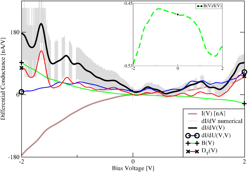
Figure 2 shows the bias dependence of the total tunneling current , calculated using Eq.(3), at the position above a surface Cr atom probed with the CrFe tip having parallel (P) magnetization direction compared to the underlying surface Cr atom. Positive current means tunneling from the tip to the sample surface, whereas the current is negative in the opposite direction. We find that the absolute value of the current is higher in the negative bias range compared to the positive range. This is due to the surface and tip electronic structures. The sample occupied PDOS combined with the tip unoccupied PDOS is greater than the sample unoccupied PDOS combined with the tip occupied PDOS, see Figure 1. Performing a numerical differentiation of with respect to , we obtain the differential conductance at this particular tip position. As can be seen this is extremely noisy, and a smoothing procedure should be applied to it before further analysis. Alternatively, the differential conductance can be calculated using Eq.(16), implemented within the atom superposition approach. Figure 2 shows that obtained this way (black curve) is a smooth function that fits precisely to the noisy numerical derivative of the current. There is more discussion about avoiding the numerical differentiation of the tunneling current in determining the , e.g. in Ref. Hofer and Garcia-Lekue (2005).
We obtain more information about the by analyzing its components, the virtual differential conductance , the background term , and the tip-derivative term . We find that differs less than 10 % compared to in the bias range [-0.01 V, +0.01V], i.e. practically at the common Fermi level of tip and sample. This means that the virtual differential conductance approximation for the (also known as the LDOS approximation) is not sufficient except at zero bias, where they are identical, . Moreover, one can recognize that most part of the peak structure is already included in the term, which is qualitatively similar to the charge PDOS of the surface Cr atom of the sample, , see Figure 1. Apart from this, the peak structure of , calculated via Eqs. (II)-(II), clearly shows up in the , particularly pronounced at high bias voltages. The reason is the rapidly changing tip electronic structure in these energy regions, see Figure 1. The features from and are transferred to the physical differential conductance, since , calculated via Eqs. (II)-(II), is smooth compared to the other two components in the whole bias range. Moreover, we find that is a monotonous function of the bias voltage, and it is nearly proportional to as has been reported earlier for different levels of STS theories Passoni et al. (2009); Donati et al. (2011). The proportionality function is plotted in the inset of Figure 2. It can be seen that its sign is in agreement with Ref. Passoni et al. (2009) and it has a non-trivial bias dependence. This is essentially due to the extra factor in the energy integration of the background term, Eqs. (II) and (II), compared to the tunneling current expression. The function could, in principle, be calculated at different tip-sample distances (), and could be compared to analytical expressions denoted by reported in Passoni et al. (2009). The comparison is, however, not straightforward due to two reasons. First, the analytical expressions were reported based on the 1D WKB approximation, whereas our model is a 3D atomic superposition approach based on WKB, which results in an effective transmission coefficient, different from the 1D WKB transmission. Note that a 3D approach to STS with another effective transmission coefficient has recently been reported by Donati et al. Donati et al. (2011). Second, in Figure 2 we reported the sum of the TOPO and MAGN contributions, while the related STS literature is concerned with nonmagnetic systems only, which corresponds to the analysis of the topographic part of the spin-polarized results. Consideration of the spin-polarized tunneling complicates the analytical calculations that are unavailable at the moment. The analysis of along the discussed lines could be a future research direction that is beyond the scope of the present study. In the following we focus on the comparison of SP-STS spectra by reversing the tip magnetization direction, and also using the flat magnetic tip model.
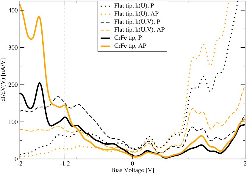
Figure 3 shows simulated single point differential conductance tunneling spectra following Eq.(16), probed with the flat magnetic tip and the model CrFe tip, above a surface Cr atom. Parallel (P) and antiparallel (AP) tip magnetization directions are set relative to the underneath surface Cr atom. It can clearly be seen that measuring the spectra with oppositely magnetized tips of the same type result in different differential conductance curves, in agreement with SP-STS experiments performed on oppositely magnetized sample areas with a fixed tip magnetization direction Yayon et al. (2007); Zhou et al. (2010). For the flat magnetic tip, two different vacuum decays, and are assumed using Eqs. (12) and (9), respectively. For the bias-independent vacuum decay (dotted curves) we find that below V, while above V. In our previous work Palotás et al. (2011) we identified the effective spin polarization [] responsible for this effect. This is the decisive factor for determining the sign of the magnetic contribution to at energy in the improved SP-STS model presented in section II as well. The magnetic part of the physical differential conductance is given in Eq.(15). Since the vacuum decay does not depend on the bias voltage for the dotted curves, and the tip is electronically flat, . Thus, the sign change of occurs at the sign change of , i.e. at the reversal of the sample spin polarization vector at 0.54 eV above the sample Fermi level Palotás et al. (2011), see also Figure 1. For the flat magnetic tip and the assumed bias dependent vacuum decay (dashed curves) we find that below V, and above V, i.e. the sign change of the magnetic component is slightly shifted toward zero bias. The reason is the nonzero background term due to , and has to be considered. Note that is still zero because of the constant tip magnetization PDOS. Comparing the two vacuum decay models for the flat tip, it is clear that the topographic part of the background term has another effect on the heights of the spectra, i.e. they are enhanced and reduced in the negative and positive bias ranges, respectively, compared to the model. On the other hand, the features of the spectra (peaks and dips) occur at the same bias positions for both vacuum decay models.
The inclusion of a realistic tip electronic structure into our model complicates the spectra even more. This is demonstrated in Figure 3 for the CrFe tip model (solid lines). In this case all three terms contribute to the differential conductance, and . Thus, the relative heights of the differential conductance tunneling spectra and are determined by the superposition of the magnetic , , and terms. The role of the effective spin polarization is more complicated, since, apart from the term, it appears in the expression through the bias-integrated quantities and . For the P tip magnetization, is the same as the black solid curve in Figure 2, and its contributions are also shown there. In Figure 3, we observe more changes of the relative height of the and spectra measured with the CrFe tip than with the flat tip. These include the sign changes of the magnetic part of the spectra, similarly as before. We find that in the bias interval [-1.04 V, +0.49 V], and a reversed relation is obtained in the complementary bias regime. Comparing the spectra to the ones measured with the flat magnetic tip, we see that they are qualitatively closer to the model used for the flat tip due to the presence of the background terms. Moreover, the individual features coming from the sample and the tip electronic structures can be assigned. In our case we identify the peak at -1.2 V, indicated by a vertical dotted line in Figure 3, coming from the CrFe tip electronic structure since it is missing from the spectra calculated with the flat tip. All other features are related to the sample electronic structure as they appear in the spectra measured with the flat tip.
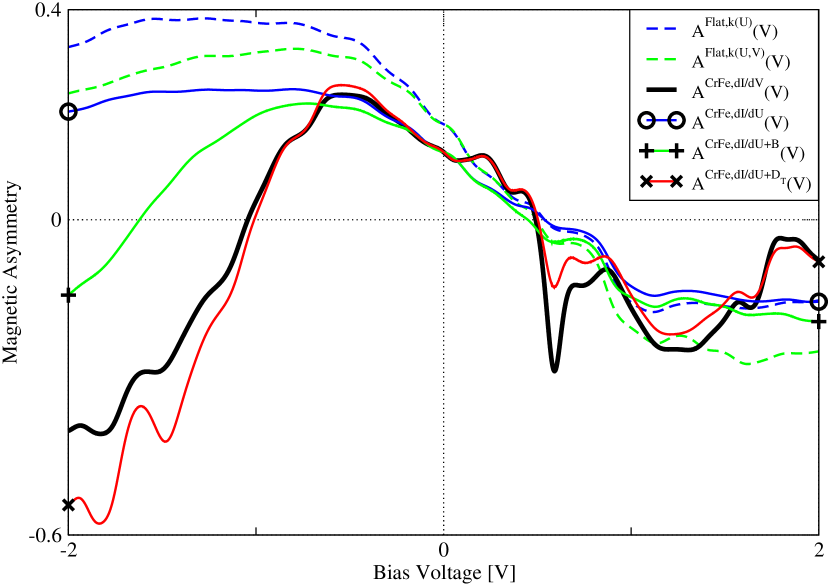
The relative heights of the differential conductance tunneling spectra and can also be determined from the magnetic asymmetry, Eq.(25). Let us compare the magnetic asymmetries calculated from the spectra in Figure 3 using the two magnetic tips. Moreover, for the CrFe tip we compare the asymmetry expressions defined in Eqs. (II)-(31), in order to estimate the error one makes when neglecting the background and tip-related components of . Figure 4 shows the calculated asymmetry functions at above a surface Cr atom. It can be seen that and (dashed curves) behave qualitatively similarly. In addition, is greater than in almost the full studied bias range. The opposite relation holds between 0 V and +0.3 V only, however, the relative difference between the two quantities is less than 1.4 % in this regime. Moreover, these two magnetic asymmetries are within 5% relative difference in the bias range [-0.23 V, +0.31 V].
Considering the CrFe tip, the experimentally measurable magnetic asymmetry (black solid curve) is qualitatively different from the two asymmetry functions calculated with the flat tip, e.g. it has a richer structure at positive bias voltages. More importantly, it has an extra sign change occurring at -1.04 V apart from +0.49 V. These correspond to the height changes of and relative to each other in Figure 3. Let us estimate the error of the magnetic asymmetry when neglecting the background and the tip-derivative terms. According to Eq.(28), (curve with symbol ’o’) considers the virtual differential conductances only. It is within 10% relative error compared to in the bias range [-0.65 V, +0.1 V]. However, its sign does not correspond to in the bias intervals [-2 V, -1.04 V] and [+0.49 V, +0.54 V]. Adding the background term to results in an improved differential conductance expression, and (curve with symbol ’+’), defined in Eq.(30), behaves qualitatively similarly to above -0.65 V. However, its sign change is shifted to +0.45 V from +0.54 V. Additionally, a sign change in the negative bias range occurs at -1.62 V. Close to the sample Fermi level, is within 10% relative error compared to in a decreased bias range of [-0.34 V, +0.1 V]. Finally, by adding the tip-derivative term to , (curve with symbol ’x’), defined in Eq.(31), shows the most closely related shape to . Furthermore, it is also quantitatively close to the physical magnetic asymmetry as its sign changes occur at -1.01 V and +0.5 V, and it is within 10% relative error compared to in an increased bias interval [-0.90 V, +0.45 V]. Summarizing this paragraph, the contribution of all three terms to the according to Eq.(16) is needed to define the physical magnetic asymmetry, that should be comparable to experiments.
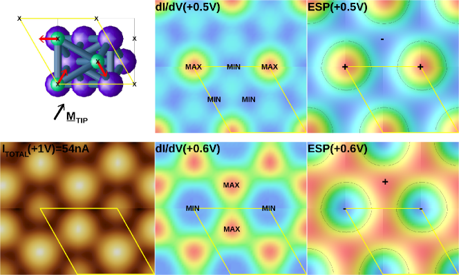
Our method presented in section II also enables one to simulate two-dimensional (2D) and magnetic asymmetry maps in high spatial resolution above the surface, that can be compared to results of SP-STS experiments. Such experiments are routinely performed while the tip follows a constant TOTAL current contour, see e.g. Ref. Kubetzka et al. (2005). Figure 5 illustrates this capability of our method, where we used the flat tip model with tip magnetization direction parallel to the direction (i.e. the magnetization direction of the surface Cr atom at the bottom left corner of the scan area, see top left part of Figure 5). Moreover, , Eq.(9) has been used for the vacuum decay. By choosing V, we calculate the 3D TOTAL current map in a box above the surface. From this 3D data we extract the current contour of nA, which is around 3.5 above the sample surface and has a corrugation of 4.2 pm. This contour, VnA is plotted in the bottom left part of Figure 5. The apparent height of the Cr atom with parallel magnetic moment to the tip is lower than those of the other two Cr atoms in the magnetic surface unit cell. This has been explained in a previous work Palotás et al. (2011). The surface scan area and the magnetic unit cell are shown in the top left part of Figure 5, indicated by a black-bordered rectangle, and a yellow (light gray) rhombus, respectively. For calculating the differential conductance-related 2D maps, we vary the vertical position of the tip apex atom following the constant current contour shown in the bottom left part of Figure 5. Thus, spin-resolved and magnetic asymmetry maps can be simulated at different bias voltages corresponding to experiments. As an example, and the effective spin polarization ESP, see Eq.(29), are shown in the middle and right columns of Figure 5, respectively, calculated at bias voltages V (top) and V (bottom). We chose these voltages close to the spin polarization reversal of the sample surface at 0.54 eV above its Fermi level, see Figure 1, and Ref. Palotás et al. (2011). Indeed, the reversal of the 2D map at V compared to V can clearly be seen. While the SP-STM image at +1 V and the map at +0.6 V show the same type of contrast, the signal is inverted for +0.5 V. Since is constant in the full energy range, this effect is due to the surface electronic structure. At +0.6 V bias, all surface Cr spin polarization vectors point opposite to their local magnetic moment directions Palotás et al. (2011), and since is set with respect to the direction (), the leading term of the magnetic differential conductance, is negative above the surface Cr atom with parallel magnetic moment to the tip. Moreover, the sign of changes to positive above the other two Cr atoms in the magnetic unit cell. This results in the minimal total above the Cr atom at the bottom left corner of the scan area (22.9 nA/V, magn. moment parallel to tip), whereas above the other two Cr atoms is maximal (23.6 nA/V, magn. moment not in line with tip). This happens even though the topographic differential conductance is higher above the Cr atom which is lower-lying on the constant current contour. Similarly, the case of +0.5 V is reversed, since all surface Cr spin polarization vectors point along their local magnetic moment directions Palotás et al. (2011) and the maximal total is achieved above the Cr atom at the bottom left corner of the scan area (16.5 nA/V, magn. moment parallel to tip), whereas above the other two Cr atoms is lower (16.0 nA/V, magn. moment not in line with tip). The minimal =15.8 nA/V is obtained above the midpoint of the lines connecting two maxima. If we introduce the notation of for the above calculated differential conductances with P parallel to the indicated in Figure 5, then the antiparallel tip orientation is denoted by AP, and can similarly be calculated. For the very same reason as discussed, a reversed tip magnetization direction would result in a reversed map concerning the heights above the non-equivalent magnetic Cr atoms. Thus, at +0.6 V the difference between and is minimal and negative above the bottom left Cr atom in the scan area, and maximal and positive above the other two Cr atoms, while the opposite is true at +0.5 V. These explain qualitatively well the simulated ESP maps, see the right column of Figure 5. The ESP contour acts as a border between surface regions with positive and negative ESP at the given bias. Note that the sign of the tip spin polarization has a crucial effect on the ESP map. Reversing the sign of compared to the direction would result in a reversed ESP map.
We suggest that by applying our method to magnetic surfaces, two-dimensional , , and magnetic asymmetry maps can be constructed on appropriate current contours at arbitrary bias, corresponding to SP-STS experiments. Similarly, an ESP map can be simulated. We stress again that the ESP can not simply be obtained from experimental magnetic asymmetry due to the presence of the background and tip-derivative terms. By explicitly considering the tip electronic structure in our SP-STS model based on experimental information, it would help in a more reasonable interpretation of experimentally measured tunneling spectra, magnetic asymmetries, and effective spin polarization.
IV Conclusions
We presented an efficient simulation method for spin-polarized scanning tunneling spectroscopy based on first principles electronic structure data within our atom superposition framework Palotás et al. (2011) by including the bias dependent background and tip-derivative terms into the differential conductance formula following Passoni et al. Passoni et al. (2009). We showed that our simulated data can be related to standard experimental setups. Taking the tip electronic structure into account, the effect of a richer variety of electronic structure properties can be investigated on the tunneling transport within the indicated approximations (atom superposition, orbital-independent spherical vacuum decay). The method is computationally cheap and it can be applied based on the results of any ab initio electronic structure code. Taking a prototype frustrated hexagonal antiferromagnetic system, a Cr monolayer on Ag(111) in a noncollinear magnetic Néel state, we simulated differential conductance tunneling spectra and magnetic asymmetries to illustrate the applicability of our method, and we analyzed the contributing terms. We found that the features of the tunneling spectra are coming from the virtual differential conductance and tip-derivative terms, and the background term is proportional to the tunneling current. We showed evidence that the tunneling spectra and the related magnetic asymmetries are sensitive to the tip electronic structure and to the vacuum decay. We also demonstrated a simulation method for 2D , magnetic asymmetry, and qualitatively correct effective spin polarization maps above a complex magnetic surface following a constant current contour. Finally, we pointed out that the magnetic asymmetry obtained from experiments can not simply be related to the sample spin polarization due to the presence of the background and tip-derivative terms.
Acknowledgments
The authors thank Paolo Ferriani and Stefan Heinze for providing the electronic structure data of the CrFe tip. Financial support of the Magyary Foundation, EEA and Norway Grants, the Hungarian Scientific Research Fund (OTKA PD83353, K77771), the Bolyai Research Grant of the Hungarian Academy of Sciences, and the New Széchenyi Plan of Hungary (Project ID: TÁMOP-4.2.2.B-10/1–2010-0009) is gratefully acknowledged.
Appendix A Theory of STS within 1D WKB
We report the formulation of the tunneling current and the differential conductance in the framework of the one-dimensional (1D) WKB approximation, which has been used in our atom superposition approach in section II. Assuming elastic tunneling, the non-spinpolarized part of the tunneling current at zero temperature is given by Ukraintsev (1996); Passoni and Bottani (2007)
| (32) |
where is the bias voltage, the tip-sample distance, an appropriate constant, the Fermi energy of the sample surface, the elementary charge, the tunneling transmission coefficient, while and are the tip and sample densities of states, respectively. Performing a change of variable from to using , the tunneling current reads
| (33) |
The applied bias voltage in the tunnel junction defines the difference between tip and sample Fermi levels, . Using this, the energy dependence of can be rewritten related to the tip Fermi level , and the tunneling current can be reformulated as
| (34) |
We denote the integrand by the formal quantity,
| (35) |
called virtual differential conductance. The tunneling current can then be expressed as
| (36) |
The physical differential conductance can be obtained as the derivative of the tunneling current with respect to the bias voltage. This can formally be written as
| (37) |
or using Eq.(35) as
This is a known formula in the literature Ukraintsev (1996); Passoni and Bottani (2007). If the tip electronic structure is assumed to be energetically flat, i.e. , which is still a widely used approximation in the recent literature, then the -dependence of disappears, i.e. , and the differential conductance becomes
Here, the second term is the so-called background term, which is a monotonous function of the bias voltage Passoni and Bottani (2007). Going beyond the assumption of the electronically flat tip by incorporating the tip electronic structure in the differential conductance expression, the effect of the tip can be studied on the tunneling spectra. The explicit energy dependence of can be calculated from first principles Ferriani et al. (2010); Palotás et al. (2011), or can be included in a model way Passoni et al. (2009). Following Eq.(A), the differential conductance can be reformulated as
Using that , the differential conductance at bias voltage can be written as a sum of three terms,
| (41) |
with
| (42) | |||||
| (43) | |||||
| (44) |
Here, is the background term usually considered in recent STS theories Passoni and Bottani (2007); Passoni et al. (2009); Donati et al. (2011), and is a term containing the energy derivative of the tip density of states (DOS), which is rarely taken into account for practical STS calculations and analyses of experimental STS data.
It can be shown that an alternative expression for the differential conductance can be derived using integration by parts,
| (45) |
with
| (46) | |||||
| (47) | |||||
| (48) |
This way another background term, enters the differential conductance formula, and the energy derivative of the sample DOS appears in the term . The average of the two expressions can also be formed as
| (49) |
which gives a third alternative form for the differential conductance within the 1D WKB approximation. On the other hand, by subtracting Eq.(45) from Eq.(41), one gets
| (50) |
This is trivial since is related to the partial derivative of with respect to :
| (51) |
From the three equivalent formulas in Eqs. (41), (45) and (49), the calculation of Eq.(41) needs the least mathematical operations, thus, we adopted this formula to our atom superposition approach in section II in order to simulate STS spectra based on electronic structure data calculated from first principles.
Finally, note that using the transmission function in Eq.(8), and the given form of the vacuum decay in Eq.(9), the derivative of the transmission probability with respect to is obtained as
| (52) |
Here, we also considered the bias-derivative of the transmission, Eq.(20). Therefore, for this particular transmission function, , and the can be expressed as
This formulation helps the better understanding of the structure of the differential conductance, and its contributing terms, and could prove to be useful for extracting information about the tip and sample electronic structures from experimentally measured spectra in the future.
References
- (1)
- Binnig et al. (1982) G. Binnig, H. Rohrer, C. Gerber, and E. Weibel, Appl. Phys. Lett. 40, 178 (1982).
- Binnig et al. (1982) G. Binnig, H. Rohrer, C. Gerber, and E. Weibel, Phys. Rev. Lett. 49, 57 (1982).
- Hofer et al. (2003) W. A. Hofer, A. S. Foster, and A. L. Shluger, Rev. Mod. Phys. 75, 1287 (2003).
- Hofer (2003) W. A. Hofer, Prog. Surf. Sci. 71, 147 (2003).
- Ukraintsev (1996) V. A. Ukraintsev, Phys. Rev. B 53, 11176 (1996).
- Koslowski et al. (2007) B. Koslowski, C. Dietrich, A. Tschetschetkin, and P. Ziemann, Phys. Rev. B 75, 035421 (2007).
- Passoni et al. (2009) M. Passoni, F. Donati, A. Li Bassi, C. S. Casari, and C. E. Bottani, Phys. Rev. B 79, 045404 (2009).
- Ziegler et al. (2009) M. Ziegler, N. Néel, A. Sperl, J. Kröger, and R. Berndt, Phys. Rev. B 80, 125402 (2009).
- Koslowski et al. (2009) B. Koslowski, H. Pfeifer, and P. Ziemann, Phys. Rev. B 80, 165419 (2009).
- Kwapiński and Jałochowski (2010) T. Kwapiński and M. Jałochowski, Surf. Sci. 604, 1752 (2010).
- Hofer and Garcia-Lekue (2005) W. A. Hofer and A. Garcia-Lekue, Phys. Rev. B 71, 085401 (2005).
- Plumer et al. (2001) E. M. L. Plumer, J. van Ek, and D. Weller, The Physics of Ultra-High Density Magnetic Recording, Springer Series in Surface Science Vol. 41 (Springer, Berlin, Germany, 2001).
- Weiss et al. (2005) N. Weiss, T. Cren, M. Epple, S. Rusponi, G. Baudot, S. Rohart, A. Tejeda, V. Repain, S. Rousset, P. Ohresser, F. Scheurer, P. Bencok, and H. Brune, Phys. Rev. Lett. 95, 157204 (2005).
- Bode (2003) M. Bode, Rep. Prog. Phys. 66, 523 (2003).
- Wiesendanger (2009) R. Wiesendanger, Rev. Mod. Phys. 81, 1495 (2009).
- Wulfhekel and Gao (2010) W. Wulfhekel and C. L. Gao, J. Phys. Condens. Matter 22, 084021 (2010).
- Serrate et al. (2010) D. Serrate, P. Ferriani, Y. Yoshida, S.-W. Hla, M. Menzel, K. von Bergmann, S. Heinze, A. Kubetzka, and R. Wiesendanger, Nature Nanotechnology 5, 350 (2010).
- Heinze et al. (2011) S. Heinze, K. von Bergmann, M. Menzel, J. Brede, A. Kubetzka, R. Wiesendanger, G. Bihlmayer, and S. Blügel, Nature Physics 7, 713 (2011).
- Yayon et al. (2007) Y. Yayon, V. W. Brar, L. Senapati, S. C. Erwin, and M. F. Crommie, Phys. Rev. Lett. 99, 067202 (2007).
- Heinrich et al. (2009) B. W. Heinrich, C. Iacovita, M. V. Rastei, L. Limot, J. P. Bucher, P. A. Ignatiev, V. S. Stepanyuk, and P. Bruno, Phys. Rev. B 79, 113401 (2009).
- Zhou et al. (2010) L. Zhou, F. Meier, J. Wiebe, and R. Wiesendanger, Phys. Rev. B 82, 012409 (2010).
- Ferriani et al. (2010) P. Ferriani, C. Lazo, and S. Heinze, Phys. Rev. B 82, 054411 (2010).
- Wiebe et al. (2011) J. Wiebe, L. Zhou, and R. Wiesendanger, J. Phys. D: Appl. Phys. 44, 464009 (2011).
- Néel et al. (2010) N. Néel, J. Kröger, and R. Berndt, Phys. Rev. B 82, 233401 (2010).
- Ternes et al. (2009) M. Ternes, A. J. Heinrich, and W.-D. Schneider, J. Phys. Condens. Matter 21, 053001 (2009).
- Schouteden et al. (2008) K. Schouteden, D. A. Muzychenko, and C. Van Haesendonck, J. Nanosci. Nanotechnol. 8, 3616 (2008).
- Heinrich et al. (2010) B. W. Heinrich, C. Iacovita, M. V. Rastei, L. Limot, P. A. Ignatiev, V. S. Stepanyuk, and J. P. Bucher, Eur. Phys. J. B 75, 49 (2010).
- Rodary et al. (2009) G. Rodary, S. Wedekind, H. Oka, D. Sander, and J. Kirschner, Appl. Phys. Lett. 95, 152513 (2009).
- Palotás et al. (2011) K. Palotás, W. A. Hofer, and L. Szunyogh, Phys. Rev. B 83, 214410 (2011).
- Hofer et al. (2008) W. A. Hofer, K. Palotás, S. Rusponi, T. Cren, and H. Brune, Phys. Rev. Lett. 100, 026806 (2008).
- Palotás et al. (2011) K. Palotás, W. A. Hofer, and L. Szunyogh, Phys. Rev. B 84, 174428 (2011).
- Wortmann et al. (2001) D. Wortmann, S. Heinze, P. Kurz, G. Bihlmayer, and S. Blügel, Phys. Rev. Lett. 86, 4132 (2001).
- Heinze (2006) S. Heinze, Appl. Phys. A 85, 407 (2006).
- Donati et al. (2011) F. Donati, S. Piccoli, C. E. Bottani, and M. Passoni, New J. Phys. 13, 053058 (2011).
- Passoni and Bottani (2007) M. Passoni and C. E. Bottani, Phys. Rev. B 76, 115404 (2007).
- Yang et al. (2002) H. Yang, A. R. Smith, M. Prikhodko, and W. R. L. Lambrecht, Phys. Rev. Lett. 89, 226101 (2002).
- Smith et al. (2004) A. R. Smith, R. Yang, H. Yang, W. R. L. Lambrecht, A. Dick, and J. Neugebauer, Surf. Sci. 561, 154 (2004).
- Tersoff and Hamann (1983) J. Tersoff and D. R. Hamann, Phys. Rev. Lett. 50, 1998 (1983).
- Tersoff and Hamann (1985) J. Tersoff and D. R. Hamann, Phys. Rev. B 31, 805 (1985).
- Chen (1990) C. J. Chen, Phys. Rev. B 42, 8841 (1990).
- Ding et al. (2003) H. F. Ding, W. Wulfhekel, J. Henk, P. Bruno, and J. Kirschner, Phys. Rev. Lett. 90, 116603 (2003).
- Tange et al. (2010) A. Tange, C. L. Gao, B. Y. Yavorsky, I. V. Maznichenko, C. Etz, A. Ernst, W. Hergert, I. Mertig, W. Wulfhekel, and J. Kirschner, Phys. Rev. B 81, 195410 (2010).
- Kresse and Furthmüller (1996a) G. Kresse and J. Furthmüller, Comput. Mater. Sci. 6, 15 (1996a).
- Kresse and Furthmüller (1996b) G. Kresse and J. Furthmüller, Phys. Rev. B 54, 11169 (1996b).
- Hafner (2008) J. Hafner, J. Comput. Chem. 29, 2044 (2008).
- Kresse and Joubert (1999) G. Kresse and D. Joubert, Phys. Rev. B 59, 1758 (1999).
- Perdew and Wang (1992) J. P. Perdew and Y. Wang, Phys. Rev. B 45, 13244 (1992).
- Hobbs et al. (2000) D. Hobbs, G. Kresse, and J. Hafner, Phys. Rev. B 62, 11556 (2000).
- Hobbs and Hafner (2000) D. Hobbs and J. Hafner, J. Phys. Condens. Matter 12, 7025 (2000).
- Monkhorst and Pack (1976) H. J. Monkhorst and J. D. Pack, Phys. Rev. B 13, 5188 (1976).
- Kubetzka et al. (2005) A. Kubetzka, P. Ferriani, M. Bode, S. Heinze, G. Bihlmayer, K. von Bergmann, O. Pietzsch, S. Blügel, and R. Wiesendanger, Phys. Rev. Lett. 94, 087204 (2005).