Also at ]NILPR, ISS, POB MG-23, RO 077125, Bucharest, Romania
Ambipolar transition voltage spectroscopy: analytical results and experimental agreement
Abstract
This work emphasizes that the transition voltages for both bias polarities () should be used to properly determine the energy offset of the molecular orbital closest to electrodes’ Fermi level and the bias asymmetry in molecular junctions. Accurate analytical formulas are deduced to estimate and solely in terms of . These estimates are validated against experiments, by showing that full experimental --curves measured by Beebe et al [Phys. Rev. Lett. 97, 026801 (2006)] and Tan et al [Appl. Phsy. Lett. 96, 013110 (2010)] for both bias polarities can be excellently reproduced.
pacs:
85.65.+h, 85.35.Gv, 73.63.-bI Introduction
Transition voltage () spectroscopy (TVS) has been recently proposed Beebe:06 to get insight into the energy offset between the metal Fermi energy and the closest molecular orbital (HOMO or LUMO), which has long been recognized to be a key quantity for the charge transport in molecular devices Datta:03 . Due to its simplicity, it soon became very popular for interpreting molecular transport measurements. Choi:08 ; Beebe:08 ; Chiu:08 ; Reed:09 ; Lee:09 ; Frisbie:10b ; Choi:10 ; Choi:10b ; Reed:10 ; Tan:10 ; Lee:11 ; Lennartz:11 Within the initial proposal relying upon a tunneling barrier picture,Beebe:06 , the minimum of the Fowler-Nordheim (FN) plot versus determined from - measurements, has been associated to the point where the barrier tilted by the applied bias change from trapezoidal to triangular. This yields .Reed:09 Later, TVS was interpreted within a coherent transport model based on a single level.Huisman:09 In the (realistic) cases where the energy offset is sufficiently larger than the level broadening due to the couplings to electrodes, the relationship deduced within the latter model ( for a symmetrical orbital location between electrodes Baldea:2010h ) turned out to be not much different from the original “barrier shape” conjecture. With certain limitations, ab initio studies Araidai:10 ; Thygesen:10b give microscopic support to the single-level model. A significant aspect in the TVS analysis Thygesen:10b is to properly account for the potential profile asymmetry. In the presence of this asymmetry, the FN-plots also become asymmetric, a fact which reflects itself in different magnitudes of the transition voltages for both bias polarities (), as pointed out recently.Molen:11b It is the main aim of this paper to consider the ambipolar TVS in detail.
The remaining part of this paper is organized as follows. The general theoretical framework will be presented in Sect. II. In Sect. III, accurate analytical formulas will be given enabling one to directly extract the quantities of physical interest from the transition voltages measured for positive and negative biases. The accuracy and the usefulness of these theoretical formulas will be illustrated in Sect. IV, by showing that applications to experimental --data yield an excellent agreement. Conclusions will be presented in Sect. V.
II Theoretical framework
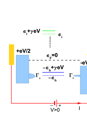
An applied bias affects the energy offset . Most easily, as currently done in electrochemistry,KuznetsovElectrocheGating:00 ; Zhang:02 ; Zhang:03 this effect can be accounted for by means of a voltage division factor Datta:03 , which specifies the bias at the location of the orbital’s “center of gravity”
| (1) |
With a potential origin as in Fig. 1, ranges from to . Eq. (1) corresponds to a potential that is flat across the molecule and entirely drops at contacts. The interfacial potential drops are
| (2) |
A positive (negative) -value corresponds to a larger (smaller) potential drop at the positive electrode, or, alternatively, to a molecular orbital energy shifted upward (downward) by a positive bias.
In the wide-band limit, wherein the transmission is Lorentzian, the current through a single level (Newns-Anderson model) can be expressed analytically as (see, e. g., Refs. HaugJauho, ; Baldea:2010e, ; Baldea:2010h, )
| (3) |
Here, is the (effective) number of molecules contributing to the current, . and , being the level broadenings due to molecule-electrode couplings. In usual cases of interest, and voltages not much higher than ,sampled-V the arguments of the inverse trigonometric functions of Eq. (3) are large, and one can approximate
| (4) |
III Useful analytical results for transition voltage spectroscopy
Eq. (4) can be used to deduce simple analytical expressions of the relevant quantities within the (realistic) assumption of a level broadening sufficiently smaller than the energy offset, which are exact to . By imposing , one obtains the transition voltages as
| (5) |
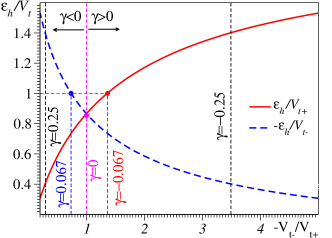
Because , it is easy to show that and . Therefore, the signs of and are opposite. Denoting by () and () the transition voltage for positive and negative polarities, and for LUMO-mediated transport (), while for HOMO-mediated transport () and . In the HOMO case, for , whereas for . For , the result for symmetric case Baldea:2010h is recovered.
Concerning the signs in general, it is worth noting that, according to Eq. (1), a redefinition of the bias polarity () yields a sign change in the division potential factor (). Therefore, the discussion can be restricted to the range, e. g., .
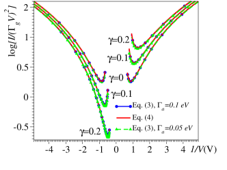
To illustrate the accuracy of the transition voltages expressed by the above analytical formulas, a comparison with the transition voltages deduced from the exact Eq. (3) is presented in Fig. 3.
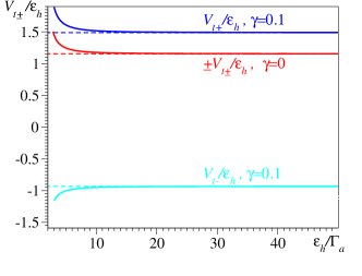
As visible there, the exact results are rapidly approached for small . Graphical results obtained by means of Eq. (5) are presented in Fig. 4 for values . In the opposite case ( ) they can be deduced by symmetry .
An important consequence of Eq. (5) is that both the voltage division factor and the energy offset can be determined from difference-molen
| (6) | |||||
| (7) |
TVS’s proof of value for molecular electronics is the fact that the FN-minimum occurs at voltages below the values corresponding to resonant tunneling where the differential conductance is maximum. This is important because, with seldom exceptions,Wandlowski:08 ; Lennartz:11 molecular junctions cannot withstand such high voltages. Still, as already noted,Beebe:08 ; Baldea:2010h it is only a small range (if at all Reed:04 ) that can be sampled in experiments. The situation can be further improved by using the minimum of a generalized FN-plot vs. ().Thygesen:11 General analytical expressions valid for arbitrary can also be deduced
| (8) |
| (9) |
| (10) |
The assignment is the same as discussed above for . The usage of -values smaller than 2 results in lower transition voltages ,Thygesen:11 which can easier be sampled experimentally. On the other side, being smaller they are more affected by the relatively large ( V Tan:10 ; Lennartz:11 ) experimental errors.
IV Discussion of experimental data
The above analytical results hold in general for the transport mediated by a single level whose energy offset is sufficiently larger than its electrode-induced broadening.
I will next apply these results to the experimental data of Refs. Beebe:06, and Tan:10, , obtained for the HOMO-mediated transport through molecular junctions in CP-AFM (conducting probe-atomic force microscopy) Beebe:06 ; Tan:10 and CW (crossed-wire) Beebe:06 setups. For a concrete comparison with experiment, it is obviously important to correctly assign, out of the two transition voltages measured for opposite bias polarities in experiment, which is and which is . Therefore, before entering into details, I note that the positive and negative biases have been chosen as the ones utilized in the experiments of Refs. Beebe:06, ; Tan:10, discussed below.
Table 1 collects the experimental data for from Refs. Beebe:06, and Tan:10, . They have been used to compute the values of and from Eqs. (6) and (7), which are also given in Table 1.
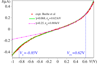
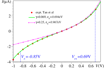
Further, I will use these values of and to reproduce the available --data for anthracenethiol- and terphenylthiol-based junctions measured in Refs. Beebe:06, and Tan:10, thanks-pramod ), respectively. To this aim, I will employ Eq. (4), which represents a very good approximation of the exact Eq. (3) for biases not too much larger than the transition voltages. The prefactor in Eq. (4) can be determined from the experimental linear conductance ( eV and eV, respectively). The theoretical curves obtained in this manner are plotted against the experimental ones in Figs. 5a and b. The agreement is excellent, and this demonstrates the remarkable accuracy of the present approach based on Eqs. (4) and (1).individual-Gammas
Table 1 shows that for the molecular junctions of Refs. Beebe:06, and Tan:10, the energy offset is, in fact, very close to the estimate of the barrier-shape conjecture if the transition voltage for positive biases is employed, .Reed:09 As visible in Fig. 4b, this does not hold in general but only for potential division factors close to .
| Molecule, platform | (V) | (V) | (eV) | |
|---|---|---|---|---|
| Anth-SH, CP-AFM a | 0.62 | -0.85 | 0.62 | 0.068 |
| Anth-SH, CW a | 0.57 | -0.85 | 0.59 | 0.086 |
| TP-SH, CP-AFM a | 0.67 | -0.82 | 0.64 | 0.044 |
| TP-SH, CP-AFM b | 0.69 | -0.85 | 0.69 | 0.069 |
| TP-SH, CW a | 0.66 | -0.92 | 0.67 | 0.071 |
Noteworthy, all the cases presented in Table 1 are characterized by small positive -values, revealing that the potential drop at the soft contact (e. g., AFM-tip) is slightly larger, [cf. Eq. (2)]. So, even a (very) small difference in the interfacial potential drops causes a significant polarity dependence of the transition voltage. This suggests that, more than the active molecule (which can differ, see Table 1), the contacts are important for the -asymmetry and calls for a systematic experimental investigation on the role of the contact groups (thiol, amine, etc).
The -values of Table 1 are significantly smaller than those estimated via DFT calculations ()Thygesen:10b and that of claimed Thygesen:11 to be appropriate for the experiments of Refs. Beebe:06, and Tan:10, . With the value , Eq. (5) yields HOMO-offsets eV (for V) and eV (for V) for the --curves shown in Refs. Beebe:06, and Tan:10, , respectively. The very small difference (much smaller than the experimental inaccuracies) between the above values and those given in Ref. Thygesen:11, ( eV and eV), deduced by assuming a Lorentzian transmission [the key assumption underlying Eq. (3)Baldea:2010e ], demonstrates again the high accuracy of the present estimates based on Eq. (4).
While the -estimates ( eV and eV deduced in the present paper versus eV and eV of Ref. Thygesen:11, ) cannot be directly checked against experiment, there is a conclusive test to decide which potential division factor ( or ) is correct. Namely, for , the transition voltages for negative bias are V and V, and they clearly disagree with the experimental data of Refs. Beebe:06, and Tan:10, , respectively.
It is worth mentioning that, as visible in Fig. 4, the / asymmetry very rapidly varies with the division potential factor . It becomes important even for small , as revealed by Table 1. Although more or less asymmetric --characteristics [] are ubiquitous in molecular electronics, such a large asymmetry (a factor ) between the positive and negative transition voltages ( V and V versus V and V, respectively) has not been reported so far.
A curious aspect should still be noted at this point. By using the values eV and eV (the curves are indistinguishable from the choice eV and eV), and , and by adjusting the prefactor in Eq. (4) to reproduce the experimental linear conductance, the agreement with experiments for positive biases is also good; see Figs. 5a and b. However, as visible there, there is a complete disagreement for negative biases.
Although the DFT inability to solve level alignment problems is well known,Neaton:06 ; Thygesen:09c it has been claimed Thygesen:10b ; Thygesen:11 that DFT-estimates of the ratio could be trusted. The DFT-values of () are based just on the fact that the ratio is determined by the value of . The above analysis reveals a further limitation of the DFT-based approaches to molecular transport, raising serious doubts on its reliability for TVS studies.
One should finally note that the above quantity is to be understood as the HOMO-offset characterizing a molecule linked to two (non-biased) electrodes. Therefore, it is not surprising that the present values ( eV and eV for anthracenthiol- and terphenylthiol-based junctions) deduced from transport data can differ from the ultraviolet photoelectron spectroscopy (UPS) data.Beebe:06 Indeed, they do differ: UPS measurements on anthracene- and terphenyl-thiol on gold yielded eV and eV.Beebe:06 Partly, the difference between and can be attributed to image effects,Schmickler:95 ; Thygesen:11 but I do not address this issue here.
V Conclusion
Although the role of the asymmetric interfacial potential drops has already been noted in the original TVS paper Beebe:06 and considered more recently,Thygesen:10b ; Thygesen:11 ; Molen:11b a direct quantitative analysis of full --curves measured in experiments has not been attempted in previous studies. The present paper shows that, by resorting to ambipolar TVS, it is possible to determine not only the energy offset (at which the original TVS aimed), but also the potential division factor without a notably increased effort: the only quantities to be determined experimentally are the transition voltages for both bias polarities. For quantitative estimates, simple, very accurate analytical formulas have been deduced, which have been excellently validated against available experimental data. The excellent agreement found in the present paper gives a strong support to the correctness of the Lorentzian transmission [the key assumption underlying Eqs. (3) and (4)] and rules out possible higher-order contributions (, etc) to the RHS of Eq. (1) for the molecular junctions investigated in Refs. Beebe:06, and Tan:10, .
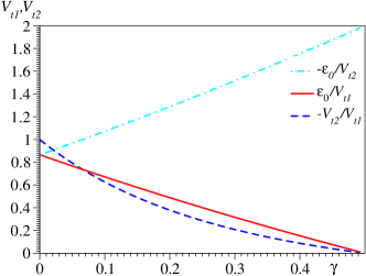
The present analysis has emphasized the need to include both bias polarities in order to obtain correct - and -estimates. In this context, a specification for the discussion Reed:11 ; Lee:11 of experimental data is helpful. According to a result of previous work,Thygesen:10b the ratio between the energy offset and the transition voltage varies from 0.86 to 2. The present paper reconfirms this result with an important specification: the aforementioned range refers to ratio , which corresponds to the transition voltage of the smallest magnitude . The ratio , which corresponds to the transition voltage of the largest magnitude , ranges from to [cf. Eq. (5) and Fig. 4a].
Acknowledgments
The author thank Horst Köppel for valuable discussions and to Pramod Reddy for providing him the raw experimental data used in Fig. 5b. Financial support for this work provided by the Deutsche Forschungsgemeinschaft (DFG) is gratefully acknowledged.
References
- (1) J. M. Beebe, B. Kim, J. W. Gadzuk, C. D. Frisbie, and J. G. Kushmerick, Phys. Rev. Lett. 97, 026801 (2006).
- (2) F. Zahid, M. Paulsson, and S. Datta, Electrical conduction through molecules, in Advanced Semiconductors and Organic Nano-Techniques, edited by H. Morkoc, volume 3, Academic Press, 2003.
- (3) S. Ho Choi, B. Kim, and C. D. Frisbie, Science 320, 1482 (2008).
- (4) J. M. Beebe, B. Kim, C. D. Frisbie, and J. G. Kushmerick, ACS Nano 2, 827 (2008).
- (5) P.-W. Chiu and S. Roth, Appl. Phys. Lett. 92, 042107 (2008).
- (6) H. Song et al., Nature 462, 1039 (2009).
- (7) G. Wang, T.-W. Kim, G. Jo, and T. Lee, J. Amer. Chem. Soc. 131, 5980 (2009).
- (8) B. Kim, J. M. Beebe, Y. Jun, X.-Y. Zhu, and C. D. Frisbie, J. Amer. Chem. Soc. 128, 4970 (2006).
- (9) S. H. Choi et al., J. Amer Chem. Soc. 132, 4358 (2010).
- (10) S. H. Choi and C. D. Frisbie, J. Amer. Chem. Soc. 132, 16191 (2010).
- (11) H. Song, Y. Kim, H. Jeong, M. A. Reed, and T. Lee, J. Phys. Chem. C 114, 20431 (2010).
- (12) A. Tan, S. Sadat, and P. Reddy, 96, 013110 (2010).
- (13) G. Wang et al., J. Phys. Chem. C 115, 17979 (2011).
- (14) M. C. Lennartz, N. Atodiresei, V. Caciuc, and S. Karthaeuser, J. Phys. Chem. C 115, 15025 (2011).
- (15) E. H. Huisman, C. M. Gued́on, B. J. van Wees, and S. J. van der Molen, Nano Letters 9, 3909 (2009).
- (16) I. Bâldea, Chem. Phys. 377, 15 (2010).
- (17) M. Araidai and M. Tsukada, Phys. Rev. B 81, 235114 (2010).
- (18) J. Chen, T. Markussen, and K. S. Thygesen, Phys. Rev. B 82, 121412 (2010).
- (19) F. Mirjani, J. M. Thijssen, and S. J. van der Molen, Phys. Rev. B 84, 115402 (2011).
- (20) A. M. Kuznetsov and J. Ulstrup, J. Phys. Chem. A 104, 11531 (2000).
- (21) J. Zhang et al., J. Phys. Chem. B 106, 1131 (2002).
- (22) J. Zhang, A. M. Kuznetsov, and J. Ulstrup, J. Electroanal. Chem. 541, 133 (2003).
- (23) H. Haug and A.-P. Jauho, Quantum Kinetics in Transport and Optics of Semiconductors, volume 123, Springer Series in Solid-State Sciences, Berlin, Heidelberg, New York, 1996.
- (24) I. Bâldea and H. Köppel, Phys. Rev. B 81, 193401 (2010).
- (25) As already noted,Beebe:08 ; Baldea:2010h with few exceptions,Lennartz:11 molecular junctions cannot withstand too large voltages and only a small range can be sampled in experiments.
- (26) Eq. (5) yields expressions different from those given without deduction in Ref. Molen:11b, . For LUMO-mediated transport, (), Ref. Molen:11b, gives , which differs from the result derived from Eq. (5). Notice that the quantity denoted by in Ref. Molen:11b, is related to the presently used (in the standard notation of electrochemistry KuznetsovElectrocheGating:00 ; Zhang:02 ; Zhang:03 ) by .
- (27) I. V. Pobelov, Z. Li, and T. Wandlowski, J. Amer. Chem. Soc. 130, 16045 (2008).
- (28) W. Wang, T. Lee, and M. A. Reed, J. Phys. Chem. B 108, 18398 (2004).
- (29) T. Markussen, J. Chen, and K. S. Thygesen, Phys. Rev. B 83, 155407 (2011).
- (30) The author thanks P. Reddy for providing him the raw experimental data of his group used in Fig. 5b.
- (31) The present method permits an upper bound () estimate of the geometrical average but not of the individual electrodes’ hybridizations ; presumably, the coupling to the soft contact is smaller . The arithmetic average could be deduced by using the exact Eq. (3) instead of Eq. (4), but the large experimental inaccuracies ( V Beebe:06 ; Tan:10 ) preclude reliable evaluations.
- (32) J. B. Neaton, M. S. Hybertsen, and S. G. Louie, Phys. Rev. Lett. 97, 216405 (2006).
- (33) J. M. Garcia-Lastra, C. Rostgaard, A. Rubio, and K. S. Thygesen, Phys. Rev. B 80, 245427 (2009).
- (34) W. Schmickler, Chem. Phys. Letters 237, 152 (1995).
- (35) H. Song, M. A. Reed, and T. Lee, Adv. Mater. 23, 1583 (2011).