Tunneling spectroscopy of the superconducting state of URu2Si2
Abstract
We present measurements of the superconducting gap of URu2Si2 made with scanning tunneling microscopy (STM) using a superconducting tip of Al. We find tunneling conductance curves with a finite value at the Fermi level. The density of states is V shaped at low energies, and the quasiparticle peaks are located at values close to the expected superconducting gap from weak coupling BCS theory. Our results point to rather opened gap structures and gap nodes on the Fermi surface.
pacs:
71.27.+a, 74.25.Jb, 74.55.+v, 74.70.TxI Introduction
Superconductivity emerges out of heavy fermions in a number of materialsFlouquet (2005); Pfleiderer (2009). Yet some of the basic fundamental properties of heavy fermion superconductors remain uncharacterized. Results from macroscopic measurements such as specific heat or thermal conductivity imply that the superconducting gap has zeros in some parts of the Fermi surface, forming the much discussed line or point nodes characteristic of unconventional or reduced symmetry superconductivityMineev and Samokhin (1999). Unconventional superconductivity is indeed likely to be favored within strongly correlated heavy electrons, to avoid mutual electron repulsion in the formation of Cooper pairs.
Recently, the application of scanning tunneling microscopy (STM) technique to heavy fermions has brought the field a significant step furtherHaule and Kotliar (2009); Schmidt et al. (2010); Aynajian et al. (2010); Hamidian et al. (2011); Suderow et al. (2004); Fischer et al. (2007); Suderow et al. (2008); Ernst et al. (2010). Attention has been turned to the so called hidden order state of URu2Si2, with the synthesis of new generation of high quality ultraclean samples in this compound Matsuda et al. (2011). The low temperature hidden order (HO) phase of URu2Si2 is indeed characterized by a low carrier density and huge entropy changes with a microscopic ordering whose nature is not yet determinedMydosh and Oppeneer (2011). If this phase was antiferromagnetically ordered, the moment magnitude would be far too small (0.02 ) to account for the large entropy changes. Thus, antiferromagnetism (AF) is believed to be not an intrinsic phenomenaMatsuda et al. (2001) but an extrinsic residual component due to the proximity of AF induced at rather low pressure (0.5GPa) or uniaxial stressAmitsuka et al. (2007); Hassinger et al. (2008); Bourdarot et al. (2011). More complex multipole ordering have been proposed: octupoleKiss and Fazekas (2005), hexadecapoleHaule and Kotliar (2009); Kusunose and Harima (2011) and dotriaecutapoleCricchio et al. (2009) with even a nematic characterIkeda (to be published). Helical Pomeranchuk orderVarma and Zhu (2006), modulated spin liquidPépin et al. (2011) hybridization waveDubi and Balatsky (2011), and rank-5 spin density waveRau and Kee (2012) have been considered. Early hints towards quadrupolar ordering have been more recently excluded using detailed experimentsRodrigo et al. (1997); Amitsuka et al. (2010). The evolution of a gap opening when entering the low temperature HO phase at THO=17.5 K has been followed in detail in atomically resolved experimentsHaule and Kotliar (2009); Schmidt et al. (2010); Aynajian et al. (2010); Hamidian et al. (2011). Hybridization between heavy quasiparticles as viewed from scattering in Th doped samples has been discussed in terms of interference effects between multiple channel tunnelingTernes et al. (2009); Yuan et al. (2011).
This peculiar ground state hosts a superconducting phase inside, whose properties are ill-known, in spite of much work since its discovery in 1985Palstra et al. (1985). Thus, the simple characterization of the superconducting state remains of great importanceAmitsuka et al. (2007); Hassinger et al. (2008); Soltan-Panahi et al. (2011); Oppeneer et al. (2010). The presence of nodes in the superconducting gap seems well established from several macroscopic experiments, such as specific heat or thermal conductivityKnetsch et al. (1992); Brison et al. (1994); Yano et al. (2008); Kasahara et al. (2009). Evidence for multiple gaps has been provided notably by the upper superconducting critical fieldDubi and Balatsky (2011); Brison et al. (1995). This is not very surprising, as the band structure is complex with sheets showing different mass renormalizationsJo et al. (2007); Oppeneer et al. (2010). The measurement of the tunneling spectroscopy of the superconducting density of states has eluded until now all experimental attacks, although early point contact experiments yielded some insightHasselbach et al. (1992); Naidyuk et al. (1996). Here we provide successful tunneling spectroscopy results in the superconducting phase. We determine values for the superconducting gap and its temperature dependence, and find a density of states, which changes as a function of the position, and has a finite value at the Fermi level.
II Experimental
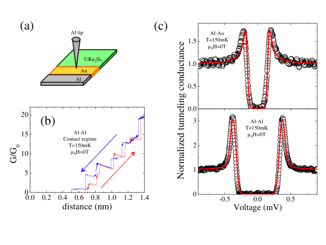
We use a STM device in a MX400 dilution refrigerator of Oxford Instruments built and tested following previous workSuderow et al. (2011); Crespo et al. (2006). We use superconducting tips of AlRodrigo et al. (2004a); Guillamon et al. (2008). These tips allow investigating, at the same time, S-URu2Si2 and N-URu2Si2 tunneling curves by measuring, respectively, at zero field and with a small magnetic field above the critical field of the Al tip (of order of 0.04 T, see Ref.Guillamon et al. (2008)). The device features a positioning system which allows to change the scanning window of 4 m2 in-situ, and to bring the tip to a sample of the same material for cleaning and preparation. We measure the tunneling current across the junction while applying a bias voltage ramp . The tunneling conductance curves versus bias voltage are obtained by numerical differentiation and are usually normalized to the conductance obtained at a bias voltage a few times above the voltage where superconducting features appear. Superconducting tips of Al are prepared and cleaned in-situ on an Al pad by mechanical annealing from repeated indentation. The scheme of the experiment is presented in Fig.1a. The tip is cleaned through an initial repeated indentation process, i.e. by inserting the tip into the sample and then making indentation and retraction repeatedly with an amplitude of some hundreds of nm using the z-piezo. When the tip is pulled out, after some thousands of repeated indentations, we observe clean conductance versus displacement curves which identify few atom Al contacts (see Fig.1b)Rodrigo et al. (2004a); Guillamon et al. (2008). The tip is totally pulled out of the Al sample, and we observe superconducting S-S tunneling curves in the current vs bias voltage curves. In clean s-wave BCS S-S tunnel junctions, simplest s-wave BCS theory gives divergent quasiparticle peaks in the conductance. The width of the actually measured quasiparticle peaks can thus be associated to the voltage jitter of the experiment Suderow et al. (2011); Crespo et al. (2006); Rodrigo et al. (2004a); Guillamon et al. (2008); Maldonado et al. (2011), for which we find here 26eV (Fig. 1c, lower panel). Once the tip has been thus characterized and the associated conductance verified to follow expected S-S features, it is moved to a clean Au sample. The N-S tunneling conductance gives then a good measurement of the lowest temperature attained in the microscope Maldonado et al. (2010). Simple BCS s-wave fits of the experimental conductance curve (Fig.1c, upper panel), give 150 mK. Finally, the tip is brought to the sample of URu2Si2 for measurement.
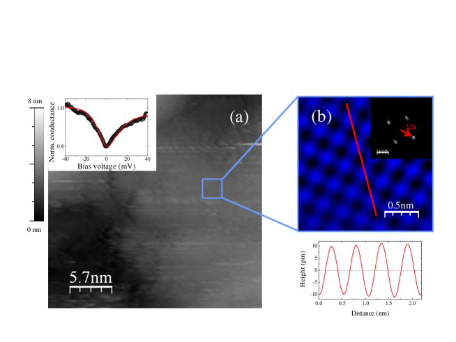
Single crystals of URu2Si2 were grown by Czochralski method in a tetra-arc furnace with argon gas atmosphere according to Ref.Matsuda et al. (2011). We decided to break URu2Si2 samples along the basal plane of the tetragonal structure at room temperature ambient conditions immediately before mounting them on the STM and cooling down. This has the disadvantage that surface contamination cannot be totally avoided, but it also allows to use a set-up suitable for superconducting tips, where the procedures described above can be performed. Moreover, the surface can be optically inspected prior to cool down and samples with nice looking surfaces can be chosen. Many materials prepared ex-situ have been found to show clean tunneling features and bulk related spectroscopic curves with a high reproducibility. Succesful experiments have been made in ex-situ cleaved, as grown and even chemically etched surfacesRodrigo et al. (1997); Suderow et al. (2008); Maggio et al. (1995); De Wilde et al. (1997); Fischer et al. (2007). Additionally, in our set-up we can macroscopically change at the lowest temperatures the scanning window without heatingSuderow et al. (2011). This allows to search in-situ over the whole mm sized sample the scanning windows (of 4m2) with best tunneling conditions. In this way, we could find in URu2Si2 scanning windows with high work functions and a clean surface providing images which are independent of the value of the tunneling current. There, we often found irregular surfaces, within which we could find small atomically flat areas. An example of the topography is shown in Fig.2. The atomic lattice of the tetragonal basal plane can be resolved (see Fig. 2(b)), with height modulations whose period corresponds to the expected basal plane lattice parameter. We observe high bias voltage Fano like features (inset of Fig.2a) due to interference between tunneling into light and heavy mass bands, characteristic of heavy fermions. These features appear above some mV and are comparable to those obtained previously Haule and Kotliar (2009); Schmidt et al. (2010); Aynajian et al. (2010); Hamidian et al. (2011); Ernst et al. (2010). In this work we focus on tunneling spectroscopy measurements at low bias voltage in order to explore the superconducting phase of URu2Si2. The typical junction conductance is of 0.4 S and the bias voltage of about 1.25mV. The tunneling curves at zero field show clean S-S’ tunneling features, which go over into N-S’ features when applying a magnetic field of 0.1 T.
III Results and discussion.
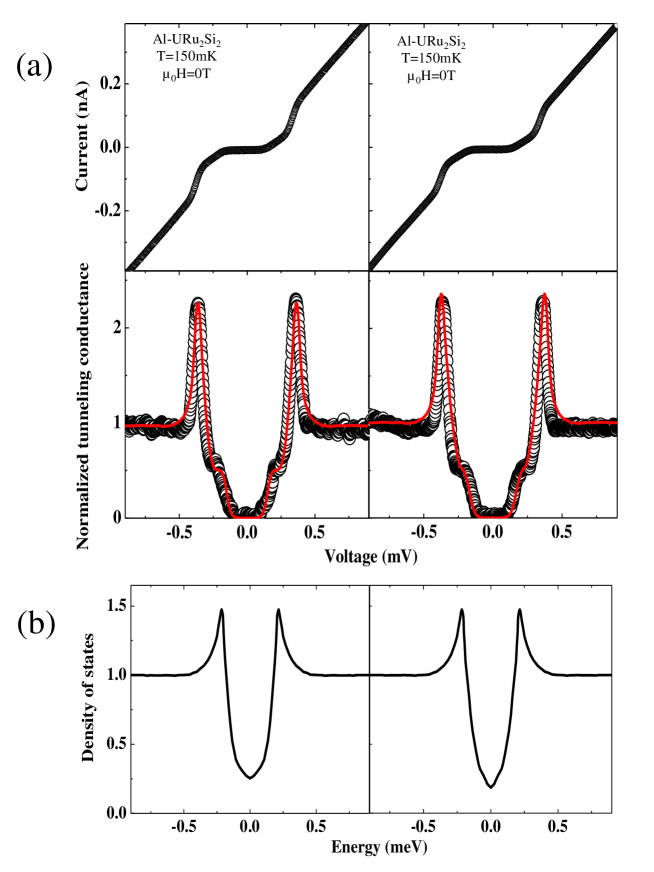
In Fig.3 we show some characteristic tunneling spectroscopy curves obtained at different positions at zero magnetic field (S-URu2Si2). The superconducting features of URu2Si2 are clearly resolved in them. These features are homogeneous over small flat areas, but, in different positions, we find slight differences, as presented in Fig.3. They appear to be related to the particular area where they were taken, and they change at scales of about 10 nm. In the S-URu2Si2 normalized tunneling conductance curves (Fig.3(a), bottom panels), we observe zero conductance at the Fermi level, resulting from the zero density of states of Al, which increases steeply above 0.2 mV, showing a pronounced shoulder. S-S’ conductance curves at very low temperatures between two s-wave BCS superconductors have a zero conductance up to the sum of both gaps, where a steep peak is found (Fig.1b and Refs.Wolf (1989); Suderow et al. (2002); Rodrigo et al. (2004b)). The presence of a marked shoulder in our experiments shows that the density of states of URu2Si2 is different from a conventional single gap s-wave superconductor.
The tunneling conductance between a superconducting tip and a sample is, in most simple single particle models, given by , where and are the respective densities of states of tip and sample, and the respective Fermi occupation functions. Using previously determined from the curves obtained when the tip is on a normal Au sample (Fig.1(c), upper panel) Rodrigo et al. (2004a); Guillamon et al. (2008), we can obtain by de-convolution from the integral, getting the curves shown in Fig.3(b). The de-convoluted curve is of course smeared and does not show noise fluctuations of the experimental conductanceGuillamon et al. (2008b). Note the peculiar low energy behavior, with a V-shaped form at low energies and well developed quasiparticle peaks. This V- shape actually produces the shoulder observed in the tunneling conductance, and shows a continuos increase of the density of states from zero energy, as expected in a superconductor with nodes in the gap function. The low but finite zero energy density of states and its changes as a function of the position can be related to band or orientation dependent tunneling into zero gap regions. The topographic features of the surface can also influence the results. More detailed measurements in large, atomically resolved areas, will be helpful to explore this further.
Application of 0.1 T drives the tip into the normal state and reveals a tunneling density of states characterized by a low but finite value close to zero energy and wide quasiparticle peaks, pointing towards a sizable distribution of values of the superconducting gap (see Fig.4). Previous reported values of the superconducting gap from tunneling spectroscopy give gap sizes several times =1.73kBTc Hasselbach et al. (1992); Naidyuk et al. (1996). Here, instead, we observe quasiparticle peaks located roughly at 0.30 meV, which is 1.36 . All this is in good agreement with the reduced jump of the specific heat derived by entropy conservationMatsuda et al. (2011).
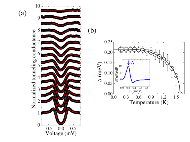
The temperature dependence of N-URu2Si2 curves is shown in Fig.5. Superconducting features of URu2Si2 disappear around 1.5 K. We can plot the temperature dependence of the density of states at the Fermi level, and of the energy for which the derivative of the density of states is maximum. Within experimental uncertainty, the latter follows roughly simple BCS theory. In the former, we do not find an appreciable temperature dependence within the uncertainty of our method. Accuracy in its determination, and the scatter found over different positions does not allow to distinguish the small difference expected between the temperature dependence of the gap value, , in a nodal superconductor and in the most simple isotropic s-wave BCS superconductorWon and Maki (1994).
Note that we find a small difference between the densities of states generally found using superconducting tips at zero field than those found using normal tips at 0.1 T. Remarkably, when the tip is normal, the quasiparticle peaks are more rounded and located at 20% higher energies and an amount of states close to the Fermi level is decreased by 10%, leading, in some particular positions, to apparently better developed BCS like curves. Interestingly, orbital pair breaking effects by the magnetic field, such as the ones produced by the presence of vortices close to the tip should lead to a decrease in the size of the gap and an increase in the Fermi level conductance, i.e. opposite as observed. Thus, either paramagnetic effects appear in the density of states, or the nodes tend to close and the gap opens in the presence of a magnetic field.
Note also that the method for obtaining the density of states discussed in Figs.3-5 is the simplest approximation for tunneling and assumes single particle tunneling. In a strongly correlated heavy fermion, simultaneous tunneling into light and heavy masses, as well as Fermi liquid effects can lead to substantial modifications of the tunneling spectra, as mentioned previously and discussed in Refs.Yazdani et al. (1997); Ternes et al. (2009); Haule and Kotliar (2009); Schmidt et al. (2010); Aynajian et al. (2010); Hamidian et al. (2011); Yuan et al. (2011) in relation with measurement at energies above the meV. It is not yet clear how these features may influence superconducting tunneling at smaller energy scales. A more detailed atomic size study simultaneously imaging high bias voltage and superconducting features would give more insight. Additionally, a theory of S-S’ tunneling where S’ is a heavy fermion may help to establish a more direct relationship between the superconducting order parameter and the features observed here in the density of states, namely, V-shape at low energies, finite value at zero energy, and slight opening when applying a magnetic field.
Other features characteristic of S-S’ junctions, such as the Josephson effect, and the temperature dependence of the S-S’ conductance curves, require a detailed analysis and more experiments. Note that the Josephson coupling energy at the tunneling conductance used here is far below the thermal energy kBT, which brings the Josephson peak below the resolution of the current measurement, even in a Al S-S junctionRodrigo et al. (2004a). Measurements at a lower tunneling conductance and as a function of temperature are under way.
Finally, let us remark that often specific heat data show a transition centered around 1.3-1.4 K, which is broad and strongly featuredMatsuda et al. (2011); Kasahara et al. (2007). The specific heat increases well above the midpoint of the transition, evidencing a reduced entropy at temperatures close to or above 1.5 K. The origin of such a featured transition has remained ill-understood. On the other hand, when applying pressure, the resistivity retains superconducting features above 0.7 GPa, where antiferromagnetism appearsHassinger et al. (2008), but no bulk superconductivity is observed in the specific heat above this pressure. Our results show that the conductance remains gapped up to 1.5 K, and that the density of states changes in different points on the surface. Remarkably, the residual term in the specific heat is small, of the order of 10%, agreeing with the observed low values of the zero energy conductance observed here. Thus, the superconducting behavior appears to be inhomogeneous, without a significant pair breaking effect affecting the low energy density of states. On the other hand, evidences for an anomalously low carrier density have been provided, and related to the hidden order gap openingBehnia et al. (2005). The low carrier density can make the superconducting properties sensitive to structural distortion. A complex order parameter, such as e.g. the suggestion of a ”chiral” state governed by the nematic HO phaseKasahara et al. (2009), could also lead to inhomogeneous superconducting behavior.
IV Conclusions.
In summary, we have measured the tunneling spectroscopy in the superconducting phase of URu2Si2 using very low temperature scanning tunneling spectroscopy. Our results are a significant instrumental step forward which will help to understand properties of heavy fermion superconductors. Although we find rather irregular surfaces, tunneling curves show opened gap structures, with values of the order of the weak coupling gap (1.73kBTc) and a small but finite density of states at the Fermi level. Finally, the finite and V-shaped density of states observed close to the Fermi level, most clearly revealed when using of a superconducting tip at zero field, points towards the presence of nodes along some directions of the Fermi surface.
V Acknowledgments.
The Laboratorio de Bajas Temperaturas is associated to the ICMM of the CSIC. This work was supported by the Spanish MICINN and MEC (Consolider Ingenio Molecular Nanoscience CSD2007-00010 program, FIS2011-23488, ACI-2009-0905 and FPU grant), by the Comunidad de Madrid through program Nanobiomagnet and by ERC (NewHeavyFermion), and French ANR projects (CORMAT, SINUS, DELICE).
References
- Flouquet (2005) J. Flouquet, Progress in Low Temperature Physics 15, 139 (2005).
- Pfleiderer (2009) C. Pfleiderer, Rev. Mod. Phys. 81, 1551 (2009).
- Mineev and Samokhin (1999) V. Mineev and T. Samokhin, Introduction to unconventional superconductivity (Gordon and Breach SV Publishers, New York, 1999).
- Haule and Kotliar (2009) K. Haule and G. Kotliar, Nature Physics 5, 796 (2009).
- Schmidt et al. (2010) A. Schmidt, M. Hamidian, P. Wahl, F. Meier, A. Balatsky, J. Garrett, T. Williams, and G. Luke, Nature 465, 570 (2010).
- Aynajian et al. (2010) P. Aynajian, E. da Silva Neto, C. Parger, Y. Huang, A. Pasupathy, J. Mydosh, and A. Yazdani, Proc. Nat’l. Acac. Sci USA 107, 10383 (2010).
- Hamidian et al. (2011) M. Hamidian, A. Schmidt, I. Firmo, M. Allan, P. Bradley, J. Garrett, T. Williams, G. Luke, Y. Dubi, A. Balatsky, et al., Proc. Nat’l. Acac. Sci USA 108, 18233 (2011).
- Suderow et al. (2004) H. Suderow, S. Vieira, J. D. Strand, S. Bud’ko, and P. C. Canfield, Phys. Rev. B 69, 060504(R) (2004).
- Suderow et al. (2008) H. Suderow, K. Behnia, I. Guillamon, V. Crespo, S. Vieira, D. Kikuchi, Y. Aoki, H. Sugawara, and H. Sato, Phys. Rev. B 77, 153101 (2008).
- Ernst et al. (2010) S. Ernst, S. Wirth, F. Steglich, Z. Fisk, J. L. Sarrao, and J. D. Thompson, Phys. Status Solidi B 247, 624-627 (2010).
- Fischer et al. (2007) O. Fischer, M. Kugler, I. Maggio-Aprile, Ch. Berthod, and Ch. Renner, Rev. Mod. Phys. 79, 353 (2007).
- Matsuda et al. (2011) T. D. Matsuda, E. Hassinger, D. Aoki, V. Taufour, G. Knebel, N. Tateiwa, E. Yamamoto, Y. Haga, Y. Onuki, Z. Fisk, et al., J. Phys. Soc. Jpn. 80, 114710 (2011).
- Mydosh and Oppeneer (2011) J. A. Mydosh and P. M. Oppeneer, Rev. Mod. Phys. 83, 1301 (2011).
- Matsuda et al. (2001) K. Matsuda, Y. Kohori, T. Kohara, K. Kuwahara, and H. Amitsuka, Phys. Rev. Lett. 87, 087203 (2001).
- Amitsuka et al. (2007) H. Amitsuka, K. Matsuda, I. Kawasaki, K. Tenya, M. Yokoyama, C. Sekine, N. Tateiwa, T. C. Kobayashi, S. Kawarazaki, and H. Yoshizawa, J. Magn. Magn. Mater. 310, 214 (2007).
- Hassinger et al. (2008) E. Hassinger, G. Knebel, K. Izawa, P. Lejay, B. Salce, and J. Flouquet, Phys. Rev. B 77, 115117 (2008).
- Bourdarot et al. (2011) F. Bourdarot, N. Martin, S. Raymond, L.-P. Regnault, D. Aoki, V. Taufour, and J. Flouquet, Phys. Rev. B 84, 184430 (2011).
- Kiss and Fazekas (2005) A. Kiss and P. Fazekas, Phys. Rev. B 71, 054415 (2005).
- Kusunose and Harima (2011) H. Kusunose and H. Harima, J. Phys. Soc. Jpn. 80, 084702 (2011).
- Cricchio et al. (2009) F. Cricchio, F. Bultmark, O. Gránás, and L. Nordstrom, Phys. Rev. Lett. 103, 107202 (2009).
- Ikeda (to be published) H. Ikeda M. Suzuki, R. Arita, et al. Nat. Phys., doi:10.1038/nphys2330 (2012).
- Varma and Zhu (2006) C. M. Varma and L. Zhu, Phys. Rev. Lett. 96, 036405 (2006).
- Pépin et al. (2011) C. Pépin, M. R. Norman, S. Burdin, and A. Ferraz, Phys. Rev. Lett. 106, 106601 (2011).
- Dubi and Balatsky (2011) Y. Dubi and A. V. Balatsky, Phys. Rev. Lett. 106, 086401 (2011).
- Rau and Kee (2012) J. Rau and H. Y. Kee, arXiV, (arXiv:1203.1047v1, 2012).
- Rodrigo et al. (1997) J. G. Rodrigo, F. Guinea, S. Vieira, and F. Aliev, Phys. Rev. B 55, 14318 (1997).
- Amitsuka et al. (2010) H. Amitsuka, T. Inami, M. Yokoyama, S. Takayama, Y. Ikeda, I. Kawasaki, Y. Homma, H. Hidaka, and T. Yanagisawa, J. Phys. Conf. Series 200, 012007 (2010).
- Yuan et al. (2011) T. Yuan, J. Figgins, and D. K. Morr, arXiv, 1101.2636 (2011).
- Ternes et al. (2009) M. Ternes, A. Heinrich, and W. Schneider, J. Phys. Cond. Matt. 21, 053001 (2009).
- Palstra et al. (1985) T. Palstra, A. Menovsky, J. van den Berg, A. Dirkmaat, P. Kes, G. Nieuwenhuys, and J. Mydosh, Phys. Rev. Lett. 55, 2727 (1985).
- Soltan-Panahi et al. (2011) P. Soltan-Panahi, D. Luhmann, J. Struck, P. Windpassinger, and K. Senstock, Nature Physics 8, 71-75 (2011).
- Oppeneer et al. (2010) P. Oppeneer, J. Rusz, S. Elgazzar, M. Suzuki, T. Durakiewicz, and J. Mydosh, Phys. Rev. B 82, 205103 (2010).
- Knetsch et al. (1992) E. Knetsch, J. Petersen, A. Menovsky, M. Meisel, G. Nieuwenhuys, and J. Mydosh, Europhys. Lett. 19, 637 (1992).
- Brison et al. (1994) J. Brison, P. Lejay, A. Buzdin, and J. Flouquet, Physica C 229, 79 (1994).
- Yano et al. (2008) K. Yano, T. Sakakibara, T. Tayama, M. Yokoyama, H. Amitsuka, Y. Homma, P. Miranovic, M. Ichioka, Y. Tsutsumi, and K. Machida, Phys. Rev. Lett. 100, 017004 (2008).
- Kasahara et al. (2009) Y. Kasahara, H. Shishido, T. Shibauchi, Y. Haga, T. Matsuda, Y. Onuki, and Y. Matsuda, New Journal of Physics 11, 055601 (2009).
- Brison et al. (1995) J. P. Brison, N. Keller, A. Vernière, P. Lejay, L. Schmidt, A. Buzdin, J. Flouquet, S. R. Julian, and G. G. Lonzarich, Physica C 250, 128 (1995).
- Jo et al. (2007) Y. Jo, L. Balicas, C. Capan, K. Behnia, P. Lejar, J. Flouquet, J. Mydosh, and P. Schlottman, Phys. Rev. Lett. 98, 166404 (2007).
- Hasselbach et al. (1992) K. Hasselbach, J. Kirtley, and P. Lejay, Phys. Rev. B 46, 5826 (1992).
- Naidyuk et al. (1996) Y. Naidyuk, H. Lohneysen, G. Goll, I. Yanson, and A. Menovsky, Europhys. Lett. 33, 557 (1996).
- Rodrigo et al. (2004a) J. G. Rodrigo, H. Suderow, and S. Vieira, Eur. Phys. J. B 40, 483 (2004a).
- Guillamon et al. (2008) I. Guillamon, H. Suderow, S. Vieira, and P. Rodiere, Physica C 468, 537 (2008).
- Suderow et al. (2011) H. Suderow, I. Guillamon, and S. Vieira, Rev. Sci. Inst. 82, 033711 (2011).
- Crespo et al. (2006) M. Crespo, H. Suderow, S. Bud’ko, P. C. Canfield, and S. Vieira, Phys. Rev. Lett. 96, 027003 (2006).
- Maldonado et al. (2011) A. Maldonado, I. Guillamon, H. Suderow, and S. Vieira, Rev. Sci. Inst. 82, 073710 (2011).
- Maldonado et al. (2010) A. Maldonado, H. Suderow, and S. Vieira, Cryogenics 50, 397-400 (2010).
- Maggio et al. (1995) I. Maggio-Aprile, Ch. Renner, A. Erb, E. Walker, and O. Fischer, Phys. Rev. Lett. 75, 2754 (1995).
- De Wilde et al. (1997) Y. De Wilde, M. Iavarone, U. Welp, V. Metlushko, A. E. Koshelev, I. Aranson, G. W. Crabtree, and P. C. Canfield, Phys. Rev. Lett. 78, 4273 (1997).
- Wolf (1989) E. Wolf, Principles of Electron Tunneling Spectroscopy (Oxford University Press, Oxford, 1989).
- Suderow et al. (2002) H. Suderow, E. Bascones, A. Izquierdo, F. Guinea, and S. Vieira, Phys. Rev. B 65, 100519(R) (2002).
- Rodrigo et al. (2004b) J. G. Rodrigo, H. Suderow, S. Vieira, E. Bascones, and F. Guinea, J. Phys.: Condens. Matter 16, R1151 (2004b).
- Guillamon et al. (2008b) I. Guillamon, H. Suderow, S. Vieira, L. Cario, P. Diener, and P. Rodiere, Phys. Rev. Lett. 101, 166407 (2008b).
- Won and Maki (1994) H. Won and K. Maki, Phys. Rev. B 49, 1397 (1994).
- Yazdani et al. (1997) A. Yazdani, B. A. Jones, C. P. Lutz, M. F. Crommie, and D. M. Eigler, Science 275, 1767 (1997).
- Kasahara et al. (2007) T. Kasahara, T. Iwasawa, H. Shidhido, T. Shibauchi, K. Behnia, Y. Haga, T. Matsuda, Y. Onuki, M. Sigrist, and Y. Matsuda, Phys Rev Lett 99, 116402 (2007).
- Behnia et al. (2005) K. Behnia, R. Bel, Y. Kasahara, Y. Nakajima, H. Jin, H. Aubin, K. Izawa, Y. Matsuda, J. Flouquet, Y. Haga, et al., Phys. Rev. Lett. 94, 156405 (2005).