Theory of band gap bowing of disordered substitutional II-VI and III-V semiconductor alloys
Abstract
For a wide class of technologically relevant compound III-V and II-VI semiconductor materials AC and BC mixed crystals (alloys) of the type AxB1-xC can be realized. As the electronic properties like the bulk band gap vary continuously with , any band gap in between that of the pure AC and BC systems can be obtained by choosing the appropriate concentration , granted that the respective ratio is miscible and thermodynamically stable. In most cases the band gap does not vary linearly with , but a pronounced bowing behavior as a function of the concentration is observed. In this paper we show that the electronic properties of such AxB1-xC semiconductors and, in particular, the band gap bowing can well be described and understood starting from empirical tight binding models for the pure AC and BC systems. The electronic properties of the AxB1-xC system can be described by choosing the tight-binding parameters of the AC or BC system with probabilities and , respectively. We demonstrate this by exact diagonalization of finite but large supercells and by means of calculations within the established coherent potential approximation (CPA). We apply this treatment to the II-VI system CdxZn1-xSe, to the III-V system InxGa1-xAs and to the III-nitride system GaxAl1-xN.
pacs:
71.20.Nr, 71.15.Ap, 71.23.-kI Introduction
Disordered semiconductor alloys of the type AxB1-xC can be experimentally realized for many technologically important semiconductor materials AC and BC (like GaAs and InAs, CdSe and ZnSe, GaN and AlN and many more) by substituting the cation A by the B counterpart. For a wide class of materials, the value can be adjusted over a large part of or even the whole concentration range, depending on the miscibility gap of the alloy system. As the electronic and optical properties vary continuously with , the electronic properties (e.g. band gap and thus emission and absorption frequency, dielectric constant, etc.) can be tailored by choosing the appropriate concentration. Therefore, these semiconductor alloys have many applications, not only as bulk semiconductors but also in low-dimensional structures like quantum wells, quantum wires and quantum dots.
In this paper, we show that the electronic properties of such substitutional semiconductor alloys of the type AxB1-xC can be described and understood on the basis of empirical tight-binding models (ETBM) for the pure semiconductors AC and BC. Once the tight-binding (TB) parameters of AC and BC are known, the ETBM for the substitutionally disordered AxB1-xC alloy is obtained by choosing the AC TB parameters with probability and the BC TB parameters with probability . The electronic eigenenergies and thus the density of states and the band gap of this disordered system can then be determined by exact diagonalization of a finite (but large) supercell. Unfortunately, it is necessary to consider a large number of microscopically distinct configurations for each concentration , as well as sufficiently large supercells, consisting of several thousand primitive unit cells at least. As this procedure is numerically expensive, we also considered and applied well established approximations for the treatment of disordered systems, namely the coherent potential approximation (CPA) and the virtual crystal approximation (VCA). While the CPA is a self-consistent Green function approximation, the much simpler (but still frequently applied) VCA corresponds to a static mean-field treatment of the disorder by replacing the randomly fluctuating potential by an average potential.
We apply our treatment to the zincblende phase of three interesting materials, namely to the II-VI semiconductor alloy system CdxZn1-xSe, to the technically established III-V alloy InxGa1-xAs and to the III-nitride system GaxAl1-xN. In a previous paper [mourad_band_2010, ] it has already been shown that the supercell exact diagonalization method yields excellent agreement with experimental results obtained for CdxZn1-xSe. But as [mourad_band_2010, ] was a joint paper together with experimentalists, the theoretical method was not yet described and discussed in detail and no comparison with CPA and VCA results for this material has been presented there. Whereas the VCA, in general, yields no band gap bowing, the CPA may even overestimate the bowing, as we will show in the present paper. We particularly present results obtained within combinations of CPA and VCA, treating the site-diagonal disorder in CPA and the off-diagonal disorder in VCA. Furthermore, we explicitly discuss the influence of a properly chosen basis set for the bowing results.
Also for InxGa1-xAs, reasonable results for the band gap bowing are obtained in agreement with literature values as obtained by experiment. For GaxAl1-xN the band gap bowing is rather small and the VCA results are not too bad at all; a crossover from a direct band gap to an indirect band gap behavior as a function of is obtained in all three applied approaches.
This paper is organized as follows: In Section II, we present the necessary theoretical background for our calculations of the electronic properties of AxB1-xC semiconductor bulk alloys. It contains a brief description of the employed tight-binding model, the CPA and the modelling on a finite ensemble of supercells. Section III contains a detailed analysis of the results that we obtained for the electronic properties of Cd0.5Zn0.5Se with the different models. Furthermore, we carefully analyze the resulting band gap bowing of CdxZn1-xSe, InxGa1-xAs and GaxAl1-xN and discuss the applicability of the CPA and VCA to these systems.
II Theory
II.1 Empirical tight-binding model for pure bulk semiconductors:
We know from textbook solid state physics that one complete basis set of the translationally invariant pure bulk system is given by the Wannier states , where is the band index and denotes the unit cell where the state is predominantly localized. The Wannier states are connected to the itinerant Bloch states , where is any wave vector in the first Brillouin zone (BZ), by means of a discrete Fourier transformation. The ETBM, as originally introduced by Slater and Koster [slater_simplified_1954, ], uses a finite linear combination of atomic orbitals on the basis sites as ansatz for the Wannier states. The matrix elements are then fitted in order to sufficiently reproduce prominent band structure features.
Because the atomic states, and hence the Wannier states, are not explicitly used in an ETBM, one has the additional freedom to directly assume a finite basis set of localized Wannier-like states. As the Wannier basis carries the translational invariance of the crystal, these states merely have to be assigned to the sites of the underlying Bravais lattice. This parametrization scheme is also known as effective bond-orbital model (EBOM) in the literature.
In this paper, we will use a basis per spin direction to reproduce bands for crystals with zincblende structure: One spin-degenerate -like conduction band (CB) and three spin-degenerate -like valence bands (VB), in detail the heavy hole (HH), light hole (LH) and split-off (SO) band. Thus, labels the sites of the underlying fcc Bravais lattice, and the TB matrix elements of the bulk Hamiltonian are
| (1) |
with the orbitals
| (2) |
The translational invariance in the pure crystal reduces the matrix problem to a problem for each [slater_simplified_1954, ], which will not be the case for disordered systems and in the later introduced supercell method. The band structure is then given by the solution of the eigenproblem
| (3) |
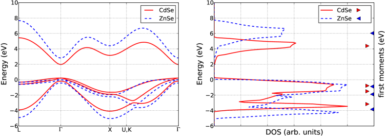
If one restricts the non-vanishing matrix elements, Eq. (1), up to a finite neighborhood and makes proper use of symmetry relations, the TB matrix elements can be expressed as a function of a set of material parameters of either the AC or BC material (e. g. CdSe and ZnSe). We will use the parametrization scheme of Loehr [loehr_improved_1994, ], which includes coupling up to second nearest neighbors. The parameters are given in the appendix. Figure 1 shows the band structure and density of states (DOS) as calculated in the EBOM for cubic CdSe and ZnSe, respectively.
Despite the small basis set, this TB model notably allows for the reproduction of a realistic bandstructure and bandwidth throughout the whole BZ. This is a typical feature of parametrizations with Wannier-like basis states [mourad_multiband_2010, ] and makes the EBOM especially suitable for the purpose of the present work, as both the CPA and the supercell calculations for the AxB1-xC alloys will require a realistic input DOS for the pure cases and as starting point—the relative position of the band centers and the bandwidths will crucially influence the alloy properties. We have also already mentioned in the introduction that the inclusion of further bands would significantly increase the computational effort. Finally, the resolution on the scale of unit cells instead of atomic sites will turn out as favorable for the simulation of the ternary AxB1-xC materials, as it will allow for an unambiguous assignment of the alloy lattice sites to either AC or BC (see Sec. II.4).
II.2 The coherent potential approximation
The basic principle of the CPA has independently been developed by several groups in the late sixties of the last century [soven_coherent-potential_1967, ][taylor_vibrational_1967, ][onodera_persistence_1968, ]. The best known formulation is certainly the work of Soven [soven_coherent-potential_1967, ], which explicitely dealt with the calculation of the electronic DOS of substitutionally disordered one-dimensional systems. An excellect and comprehensive general introduction into the CPA formalism can be found in [matsubara_structure_1982, ].
The simplest form of the CPA for an alloy assumes uncorrelated substitutional disorder of the respective species. If all sites are indistinguishable (i. e. no division into sublattices is necessary), as it is the case in the spatial discretization in the EBOM, the probability of finding either species is just given by the concentrations and .
For the sake of clarity, we will supress the band and orbital indices until further notice. In order to be consistent with the common CPA literature, let us denote the site diagonal () TB matrix elements of the AC or BC material as :
We will now briefly specify the most important assumptions that enter the CPA (see e. g. [matsubara_structure_1982, ] for details of the derivation):
-
1.
The disorder is confined to the diagonal elements. The off-diagonal (or hopping) matrix elements with are either identical for both species or can approximately be replaced by a common value, e. g. the VCA average. If we now separate the TB Hamiltonian of the alloy into a diagonal part and an off-diagonal part , such that , only is site-dependent, as , depending on the species on the site . The operator is still translationally invariant under translations by and therefore remains diagonal with respect to Bloch states .
-
2.
The configurational average over the resolvent of defines an effective Hamiltonian :
(4) Here, is the identity operator and is in the complex energy plane, containing the energy axis . The self-energy operator absorbs the influence of the disorder on the microscopic scale. Note that will in general be non-hermitian.
-
3.
Due to the single-site nature of the CPA, the self-energy is diagonal in every representation. Furthermore, its matrix elements are neither dependent on nor on .
In order to obtain the self energy matrix elements , which uniquely define the effective medium, we have to solve the CPA equation for two constituents:
| (5) |
The complex-valued is the configurationally averaged one-particle Green function in Wannier representation (more precisely its -diagonal element). Although does not depend on in the CPA, we will keep the index to clearly distinguish it from its Bloch representation . The two representations are connected by
| (6) | |||||
with as the number of wave vectors in the first BZ or the corresponding irreducible wedge (as and , this relation follows directly from the invariance of the trace under unitary transformations).
Under certain conditions, the summation over all -values can be avoided by the introduction of a sufficiently smooth DOS for the off-diagonal part :
| (7) |
Now the calculation of can be performed as a one-dimensional integration/summation over the energy axis:
The approximation holds if is approximately constant on the interval .
The equations (5) and optionally (6) or (II.2) can be solved in a self-consisted manner in order to obtain and . We can then directly obtain further quantities for the effective medium; e. g. the configurationally averaged DOS per lattice site is given as
| (9) | |||||
As a rule of thumb, the CPA is known to yield very good results in two limit cases [matsubara_structure_1982, ]:
-
1.
The weak scattering limit, where the difference of the first moments of the substituents (aka the centers of gravity of the bands) is smaller than the respective bandwidths.
-
2.
The split band limit or atomic limit, where the substituents’ first moments are either sufficiently far apart or the bandwidths are small, so that the respective bands do not overlap.
Additionally, it of course also gives the correct pure limit for and . Also, in the limit case of vanishing difference of the moments, the CPA reduces to the VCA.
II.3 Multiband CPA + ETBM
The formal extension of the CPA to multiband TB models is straightforward and has been used in different levels of detail to qualitatively examine the electronic properties of disordered alloys (see e. g. [stroud_band_1970, ][krishnamurthy_band_1986, ] for SixGe1-x, [faulkner_electronic_1976, ] for PdxH1-x, [hass_electronic_1983, ] for CdxHg1-xTe or [laufer_tight-binding_1987, ] for palladium-noble-metal alloys).
II.3.1 representation
In the EBOM, the localized basis is now given by the TB orbitals . Hence, Eq. (5) has to be replaced by the corresponding matrix equation, with
| (10) | |||||
as matrices per spin direction (here, the square brackets denote matrices). The effective Hamiltonian matrix in the TB scheme can be obtained by the substitutions
| (11) | |||||
| (12) |
i. e. the hopping matrix elements are approximated in the VCA. Like in Eq. (6), we then obtain the Green function via BZ summation,
| (13) |
where is the identity matrix. The matrix has non-vanishing off-diagonal elements , as the TB Hamiltonian is not diagonal in the orbital basis .
II.3.2 Band-diagonal (Wannier) representation
Alternatively, we can again calculate Green’s function via energy integration. In a
band-diagonal (Wannier-like) TB representation,
the site-diagonal TB matrix element
of the -th band can be calculated from the first moment
| (14) |
with as the DOS of band (normalized to unity). Therefore, we can assign the moments of the AC or BC system to a corresponding self-energy:
| (15) |
The analogon of equation (II.2) is then the band-diagonal Green function matrix (denoted by “wn” for “Wannier” from now on) with elements
| (16) | |||||
with as the VCA DOS of the -th band, shifted by . This procedure allows us to calculate the DOS of the off-diagonal operator in the Wannier basis by diagonalization of the EBOM Hamiltonian in the VCA. Notably, we do not have to explicitly know the corresponding matrix elements .
II.3.3 Calculation of electronic properties
Finally, the CPA + ETBM DOS of the alloy can be calculated by either tracing over the orbital index (in the basis) or the band index (in the Wannier basis) of the matrix elements:
| (17) | |||||
| (18) |
Although the trace of a matrix is of course independent of the representation used, it should be noted that and are not identical: The self-energies, which define the effective medium, replace different quantities [see Eqs. (11) and (15)], which results in different operators .
Due to the translational invariance of the self energy matrix elements and thus , we can define a complex band structure of the medium. The electronic excitations of the effective medium can be assigned to quasiparticles with a modified dispersion relation
| (19) |
The corresponding CPA one-particle spectral function
| (20) |
will in general be broadened in case of disorder , as the non-vanishing imaginary part of accounts for a finite lifetime of the excitation.
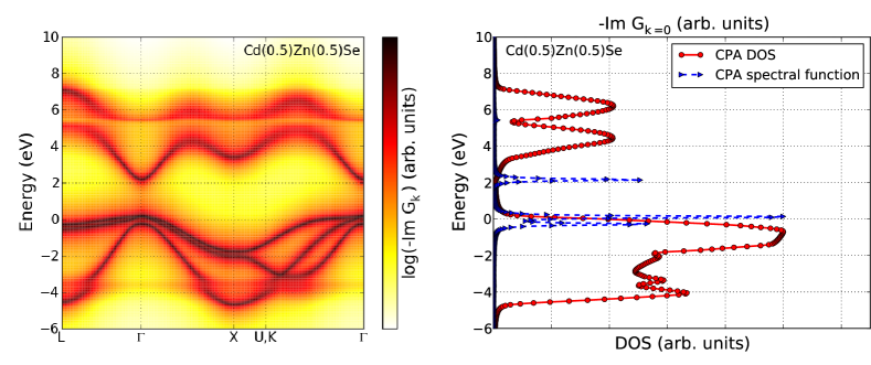
As an example, Fig. 2 visualizes the complex band structure of Cd0.5Zn0.5Se on the left, calculated in the combination of the CPA and the EBOM. On this energy scale over the whole bandwidth, the results from the Wannier and the representation are not distinguishable. The color-coding clearly shows the -dependent broadening of the band structure due to finite lifetime effects. The figure on the right additionally shows the corresponding CPA DOS and the spectral function at the BZ center for all four spin-degenerate bands, i. e.
Note that we have chosen a relatively large imaginary part for the energy axis, which leads to a small but non-vanishing DOS in the band gap region. We furthermore used values in the irreducible BZ of the fcc lattice. The peak structure of the quasiparticle excitations at the edges of the band gap region is clearly visible. A qualitative and quantitative discussion of the electronic structure in comparison with VCA and supercell results will follow in Section III.1.
II.4 Supercell tight-binding calculation in the EBOM
If the Hamilton operator is no longer translationally invariant, the TB approach is not reducable to the form (3) and we are left with the matrix eigenvalue equation
| (21) |
We will now use a finite supercell with periodic boundary conditions. Like in calculations for zero-dimensional nanostructures [marquardt_comparison_2008, ][schulz_multiband_2009, ][mourad_multiband_2010, ][mourad_multiband_2010-1, ], we will furthermore assume that
| (22) |
Again assuming uncorrelated substitutional disorder in the AxB1-xC alloy, each primitive cell will be occupied by the AC or BC basis, where the probability of finding either an AC or BC pair in the unit cell at is directly given by the concentrations and . Building the Hamilton matrix for the supercell, we will therefore use the matrix elements of the pure AC or BC material for the corresponding lattice sites. The valence band offset between the two materials is incorporated by shifting the respective site-diagonal matrix elements by a value . Hopping matrix elements between unit cells of different material are approximated by the arithmetic average of the corresponding AC or BC values. Although this approach for the incorporation of the energy offset and the hopping between two materials is very simple, it gives the correct limit in the pure case. In the phase separation case (a limit of which the propability is practically zero in case of uncorrelated disorder), it would furthermore lead to an interface treatment that has been extensively tested in calculations for low-dimensional heterostructures [marquardt_comparison_2008, ][schulz_multiband_2009, ][mourad_multiband_2010, ]. Specifically, the results turn out to be insensitive to small variations of the hopping between two materials (e. g. the usage of a geometric instead of an arithmetic average).
The usage of the EBOM, i. e. the usage of Wannier-like orbitals situated at the sites of the Bravais lattice in the supercell approach, has several advantages over similar approaches which use an ETBM with discretization on atomic sites:
-
1.
Even when introducing disorder on a microscopic scale, each lattice site can be unambigously assigned to one site-diagonal TB matrix element and the corresponding band structure parametrization for either AC or BC. In ETBM supercell calculations with atomic resolution, each anion of the type C will locally be surrounded by a different number of A or B cations, thus making an assignment of the diagonal elements of the anions to the band structure of either AC or BC impossible.
It is common to then use either a concentrationally averaged VCA value or to determine this matrix element as a weighted average of the C matrix elements for AC and BC, depending upon the number of nearest-neighbour atoms A or B [tit_absence_2009, ][boykin_approximate_2007, ]. This will lead to an effectively more coarse-grained resolution as in the case of the EBOM, as the latter model only has to average the intersite hopping matrix elements (which typically differ on a scale of in materials with moderate lattice mismatch). In the CdxZn1-xSe system for example, the site diagonal matrix elements for the Se anions in CdSe and ZnSe (see e. g. Refs. [tit_absence_2009, ] and [schulz_tight-binding_2005, ]) differ to a larger extent than the EBOM hopping matrix elements when using a congruent set of input parameters.
-
2.
All influences which originate from effects on a smaller length scale, like the difference in the AC and BC bond lengths, are absorbed into the values of the corresponding TB matrix elements between the effective orbitals.
-
3.
As the results are not sensitive to the exact treatment of the hopping between AC and BC sites, further effects that basically result in minor variations of the hopping matrix elements (like small bond angle changes due to relaxation) can be neglected in a first approximation.
The numerical diagonalization (e. g. using standard numerical libraries like ARPACK/PARPACK) of the corresponding Hamiltonian for a fixed concentration and a finite number of microscopically distinct configurations gives the density of states (DOS) of the finite ensemble. In order to obtain a meaningful DOS from the supercell calculations, we must first appropriately define it. Strictly speaking, a macroscopic alloy crystal represents just one realization; by dividing it into small portions, we can nevertheless get subsystems that differ from each other on a microscopic scale. In this sense, the DOS for one fixed concentration is then obtained by the average of the DOS for each finite ensemble.
To eliminate the influence of finite size effects, the number of lattice sites as well as the ensemble size must be sufficiently large. We point to previous work [mourad_band_2010, ] for a careful analysis of the convergency behaviour and will use the recommendations throughout this paper. In a nutshell, a resolution of the band edges up to , which is the typical input accuracy for the material parameters, will require supercells with – lattice sites and 0 microscopically distinct configurations per concentration. For a discussion of properties on a larger energy scale, e. g. a comparison of the DOS over the whole bandwidth, smaller supercells and ensemble sizes can be chosen.
In contrast to the CPA, the supercell approach can easily be augmented to simulate effects not only of configurational, but also of concentrational disorder. This can easily be achieved when we drop the constraint that the overall concentration of AC sites per configuration should equal the point probability and occupy each lattice site independently. In the limit of large , we will of course have , so that the constraint is fulfilled for sufficiently large ensemble numbers. For most cases, this is closer to experimental reality anyway, as concentration values are commonly averages over macroscopic volumes, e. g. by means of X-ray diffraction [mourad_band_2010, ]. It also allows us to perform calculations for concentration values where .
III Results
In this section, we will apply the CPA EBOM and the supercell EBOM to cubic CdxZn1-xSe, InxGa1-xAs and GaxAl1-xN. In addition, we will also add results that are obtained by a pure VCA calculation.
Besides the fact that we have already shown the reliability of the supercell EBOM for cubic CdxZn1-xSe in comparison with experimental results in [mourad_band_2010, ] (albeit for slightly different material parameters to meet the experimental boundary conditions), this material systems is also especially interesting for a quantitative and qualitative analysis of the applicability of the CPA. A closer look at the DOS and the energetic position of the first moments in Fig. 1 reveals that the conduction bands of CdSe and ZnSe neither fulfill the weak scattering nor the split band condition very well, as the energetic range of the overlap is comparable to the difference of the first moments. The InxGa1-xAs system under consideration will in contrast be closer to the weak scattering limit. This condition will also apply to the zincblende GaxAl1-xN alloy, which additionally comprises a direct-indirect band gap transition at a certain mixing ratio.
III.1 Comparison of the overall density of states of Cd0.5Zn0.5Se
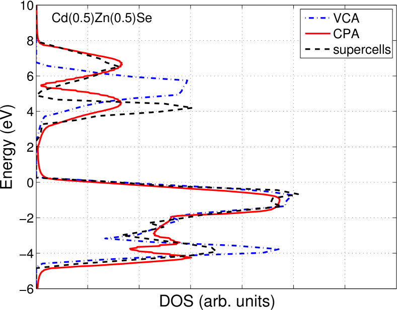
In this section, we will compare the overall DOS of the AxB1-xC alloy as calculated with the CPA and the supercell EBOM, using the example of Cd0.5Zn0.5Se, along with results from the simple VCA. The supercell calculations were performed with 20 microscopically distinct configurations and on cubic supercells with 2048 lattice sites, i. e. 4096 atoms; the numerical parameters for the CPA calculation match those of Fig. 2.
Overall, the alloy DOS of the valence bands is very similar in all three models. This is not very surprising, as the substitutional disorder is restricted to the cations of the material, and the valence bands mainly stem from atomic -orbitals of the Se anions. However, the conduction band DOS accordingly shows different features in the three models.
It is clearly visible that the VCA DOS is an interpolation of the DOS of the pure CdSe and ZnSe material as depicted in Fig. 1; aside from an energetic shift of the bands, no new features arise for the alloy material.
Contrary to the VCA, the CPA gives a DOS with qualitative and quantitative features that exceed the results of simple interpolation schemes by far. The conduction band visibly splits into two subbands. When the resolution is further increased, a quasi-gap can be identified. The relative spectral weight of the two subbands is exactly given by the concentration ratio of of the substituents (this also holds for all other values of with identifiable subband splittings).
Like in the CPA, the supercell EBOM also gives an alloy DOS of which the structure is more complicated than the DOS of the constituents. The conduction band DOS again splits into a two-subband structure, where the relative spectral weight equals the concentration ratio of the substituents. Furthermore, the two subbands can now clearly be distinguished by a difference in their shape. Additionally, the quasi-gap is located at a lower energy than in the CPA.
Overall, the fact that VCA totally fails to reproduce the additional features of the alloy’s conduction band was to be expected; the one-electron potential which enters the hopping matrix elements is not a self-averaging quantity (in the sense that it can be replaced by its ensemble average for a sufficiently large sample), as opposed to the one-electron Green’s function [kohn_quantum_1957, ].
The artificial symmetry in the conduction subband structure in the CPA is an artefact of the usage of concentrationally dependent, but nevertheless common intersite hoppings. This mean-field approach for the hopping matrix elements directly carries over to the shape of the DOS (this can most easily be seen in the Wannier basis, as the shape and the bandwidth is eventually determined by the hopping elements, while the band moments are given by the site-diagonal elements, see Sec. II.3.2).
III.2 Comparison of the band gap bowing of CdxZn1-xSe
We will now extensively examine the accuracy of the CPA approach for properties on a smaller energy scale and use the example of the single-particle band gap for a qualitative as well as quantitative analysis.
Most alloyed bulk semiconductors show a more or less pronounced bowing of the band gap as a function of the concentration . The simplest way to describe the deviation from a linear behaviour is the assumption of a parabolic curve and therefore the use of a single, concentration-independent bowing parameter , such that
| (23) |
Here, the indices AC and BC assign the properties of the pure binary materials. In general, the literature values for show a surprisingly large variety even for apparently comparable experimental conditions (the reader may check comprehensive review articles like [vurgaftman_band_2001, ] or [vurgaftman_band_2003, ]). For the II-VI bulk alloy CdxZn1-xSe for example, a broad range of values between and has been reported throughout publications from the last two decades [tit_absence_2009, ] [ammar_structural_2001, ][venugopal_photoluminescence_2006, ] [gupta_optical_1995, ]. The large disparity on the experimental side can for example result from difficult growth conditions for the mixed systems. On the theoretical side, the inadequate use of too simple approaches like the VCA can lead to wrong results.
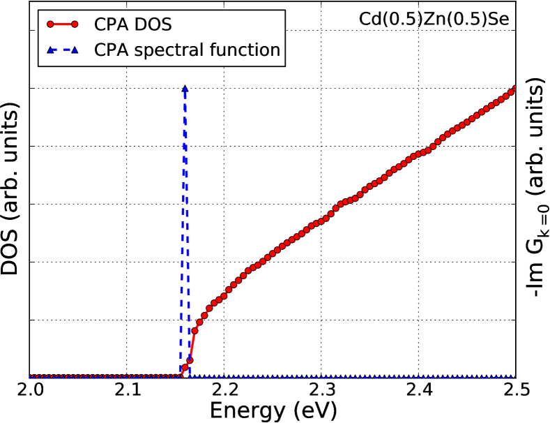
In the CPA, the band gap can in principle be read off from the DOS. For numerical reasons, the CPA DOS will not completely fall to zero in the bandgap, as a finite imaginary part of the energy is required. Nevertheless, it is possible to identify the band gap with desired accuracy by increasing the resolution. We used an imaginary part of and values in the irreducible BZ. The high BZ resolution has turned out to be crucial to obtain convergence for the results for the band gap. In the Wannier representation, it is furthermore very important to carefully discretize the VCA DOS when using Eq. (16) because the DOS will contain kinks that stem from Van Hove singularities [critical points where ]. The usage of TB models that give a reliable band structure throughout the whole BZ (in contrast to dispersions from effective mass or models) will additionally lead to sharp peaks at some of these critical points, as the slope of non-degenerate bands must also vanish at the BZ boundaries.
Figure 4 shows the conduction band edge region of Cd0.5Zn0.5Se, calculated in the Wannier CPA. The peak of spectral function of the quasiparticle obviously coincides with the band edge within the chosen energy resolution of . A further analysis (not shown) reveals that the CPA band edge states are mostly -like; in case of broadened peaks, the corresponding linewidth is so small that the peak position still allows for a convenient determination of the conduction band edge and the valence band edge with an accuracy of . Hence, the band gap of the alloy can be determined with an accuracy of 0.02 .
The corresponding supercell band gap is given by
| (24) |
where again numbers the distinct configurations. Note that this definition of the band gap implies
| (25) |
i. e. the band gap of the disordered alloy is different from the configurational average over the energy gaps for fixed realizations .
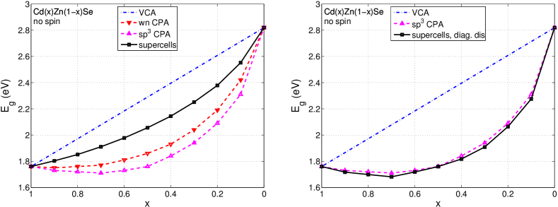
The resulting curves for the CdxZn1-xSe band gap are depicted in Fig. 5. In order to perform a detailed examination of the influence of the disorder and the applicability of the CPA, we performed two different supercell calculations for the CdxZn1-xSe alloy system. In order to get rid of finite size effects, we used supercells with lattice sites and calculated the band edges for distinct configurations per concentration. The concentration itself is varied in steps of 0.1.
The left subfigure contains results from the supercell EBOM exactly as described in Sec. II.4, thus including the full disorder in the site-diagonal and the hopping matrix elements on the microscopic scale. The supercell results in the right subfigure have been obtained under the artificial restriction to site-diagonal disorder. This means that only the site-diagonal matrix elements differ throughout the cell and with each configuration, while the hopping matrix elements for each concentration were substituted by their VCA values. Both the supercell approach and the CPA then use the same level of mean-field approximation for the hopping matrix elements. As each of supercell bowing curve requires the partial diagonalization of Hamiltonian matrices (the and values are input material parameters), we additionally neglected the spin-orbit coupling for this comparison. Besides an increase in computation time by a factor , the memory comsumption is lowered, as all matrix entries are then real numbers. We also added the pure VCA results to both figures—as the tight-binding matrix is diagonal at , we are left with a linear curve, which is at least able to indicate the deviation of the other results from a linear interpolation.
We will first turn to the full disorder case on the left. Overall, the bowing obtained in the CPA is clearly larger than the corresponding supercell result. When the Wannier representation is used, the bowing curve is slightly closer to the supercell case than in the basis. This was to be expected, as the overall shapes and bandwidths of the pure CdSe and ZnSe bands are very much alike (see again Fig. 1). Nevertheless, the CPA (as well as the VCA) fails to satisfactorily reproduce the supercell band gaps over the whole concentration range. We can even identify a slight “overbowing”, where the CPA band gap of the alloy dips beneath the value for pure CdSe for the Cd-rich concentrations. This effect is ultimately a consequence of the usage of the concentration-dependent VCA average for the non-diagonal part of the Hamilton. Consequently, it does not occur in standard textbook examples, where the same hopping values for the constituents are used and one is left with a concentration-independent bandwidth.
A look at the right subfigure, where the supercell results with diagonal disorder are given along with the CPA curve, clearly reveals the importance of the non-diagonal part (as the supercell potential lacks translational invariance, our supercell TB model can only be used in the basis, so that the Wannier CPA results are also not given again here). We easily notice that the CPA and supercell results now coincide very well. Consequently, we can state that the CPA can in principle simulate the influence of the disorder in the site-diagonal elements on the band gap and the deviations stem from the mean-field treatment for the hopping. If we enforce the constraint for single concentration values and thus eliminate the small influence of concentrational disorder (see Sec. II.4) on the supercell results, the discrepancy is even smaller (not shown).
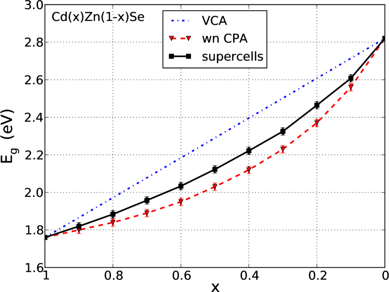
For the sake of completeness, we depict the Wannier CPA and supercell results including spin-orbit interaction in Fig. 6 (the CPA results will be omitted from now on). We also added errorbars that account for the reading accuracy and finite size effects. The difference in the first moments of the CdSe and ZnSe conduction bands turns out to be slightly smaller when the spin is included. Obviously, the bowing is reduced and the deviation between the Wannier CPA and supercell results decreases further. Still, only the results overlap within the error range. The best possible second-order fit to the curve yields a bowing parameter of for the supercell results and for the curve as calculated with the Wannier CPA (note that the bowing values in [mourad_band_2010, ] were calculated for slightly differing band gap values in the pure case). It should be emphasized that the error range for the bowing values can only account for the influence of the reading accuracy and finite size effects, as well as for the deviation from a parabolic behaviour (this is always to be expected for differing lattice constants, see [richardson_dielectric_1973, ]). The disparities that can arise from the uncertainty in the input parameters for the pure materials (band gaps, effective masses, valence band offsets) from different sources in the literature cannot reliably be estimated at reasonable expense, so that the error range is certainly underestimated.
III.3 Band gap bowing of InxGa1-xAs
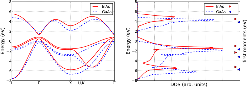
As a second example for the calculation of the band gap bowing, we apply the methods to the zincblende bulk alloy InxGa1-xAs. The band structures, DOS and corresponding first moments of InAs and GaAs are given in Fig. 7. A valence band offset of [pryor_eight-band_1998, ] has already been incorporated. This value has been obtained by the relative energetic position to transition-metal impurities and is in agreement with experimental data from measurements on Au Schottky barriers [tiwari_empirical_1992, ].
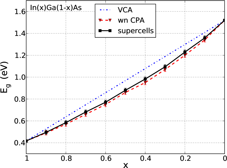
For this parameter set of InAs and GaAs the first moments of the conduction band are closer together than in the case of CdSe and ZnSe, going along with a larger overlap of the bands. Hence, we are closer to the weak scattering condition and therefore expect better results for the concentration-dependent band gap from the (Wannier) CPA. Again using configurations and lattice sites for the supercells and also the same numerical parameters for the Wannier CPA, we obtain the bowing curve depicted in Fig. 8.
Overall, the deviation from a linear behaviour (again indicated by the VCA results) is smaller for InxGa1-xAs than for CdxZn1-xSe. Furthermore, all results from the supercell calculations and the CPA calculations now overlap within the error range, although the CPA still slightly overestimates the bowing behaviour. A second-order fit of the values gives a bowing of for the supercell results and for the curve as calculated with the Wannier CPA. The fact that the resulting ranges touch but do not overlap is mainly due to the deviation from a parabolic curve. Nevertheless, including the error boundaries both values lie in the range between – that is recommended in the literature by Vurgaftman et al. in [vurgaftman_band_2001, ]. More recent ab initio calculations within the DFT+LDA (which are known to systematically underestimate the band gap) give a slightly larger bowing in the range of – stroppa_composition_2005 .
III.4 Band gap bowing of GaxAl1-xN
As a final example, we will calculate the concentration dependent band gap of the zincblende phase of GaxAl1-xN, which is frequently used as barrier material in optoelectronics [vurgaftman_band_2001, ]. While the wurtzite modification of AlN is the only Al-containing III-V semiconductor with a direct band gap, its zincblende modification is most likely indirect with the conduction band minimum at the -point and the valence band maximum at the -point [fritsch_band-structure_2003, (although a direct band gap is sometimes also assumed, see e. g. [fonoberov_excitonic_2003, ). As can be seen in Fig. 9, the EBOM is able to reproduce the indirect band gap of AlN properly, as it is also fitted to the -point energies. We use a valence band offset of [vurgaftman_band_2001, ][vurgaftman_band_2003, ]; the resulting relative positions of the first moments and the large conduction band overlap indicate again a good applicability of the CPA. In contrast to the previous material systems, the spin-orbit coupling is one order of magnitude smaller in the nitride compounds and does not influence the results for the bowing.
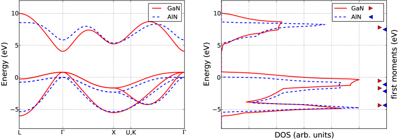
The results for GaxAl1-xN are depicted in Fig. 10. The numerical parameters for the CPA and the supercell calculations were chosen identical to those of the previous sections. In all three models, we can clearly identify a crossover in the bowing between and . In this region, the character of the band gap changes from a behaviour which is strongly influenced by the indirect AlN material to a direct band gap behaviour dominated by GaN.
While the CPA results coincide very well with the supercell results for the GaN-dominated side at large , they overestimate the bowing on the Al-rich side. In contrast, the VCA, which shows a piecewise linear behaviour with two different slopes, can reproduce the supercell results for high Al contents quite well, but deviates for . It additionally should be noted that the CPA results in the Al-rich part have larger error bars, as the determination of the band gap is afflicted with a larger uncertainty in this range due to a larger broadening of the corresponding spectral functions (not shown).
In [vurgaftman_band_2003, ], Vurgaftman et al. report bowing parameters of – for the -valley of cubic GaxAl1-xN from theory. By additionally taking several experimental results into account (which obviously render larger bowing parameters), they recommend an approximate value of . By only fitting the -valley bowing, i. e. only taking the values for into account, augmented by the AlN energy difference at as boundary value, we obtain bowing parameters of from the supercell calculations and from the CPA. Consequently, the CPA and supercell values agree within the error range and our results are in reasonably good agreement with the literature values. More recent results from DFT+LDA calculations [kanoun_ab_2005, ] yield a value of and predict the crossover at about . However, it should be noted that these results suffer from the usual underestimation of band gaps in DFT+LDA. The pure GaN and AlN band gaps in their calculations are obtained as 1.93 and 3.23 respectively. Consequently, they strongly deviate from our input values of 3.26 for GaN and 5.346 for AlN (see appendix), as our CPA/supercell + EBOM model allows for the usage of arbitrarily exact boundary values at and .
For the sake of comparison, we summed up the results for the bowing parameters in Tab. 1. As already stated, the given error ranges only account for the reading accuracy, finite size effects and non-parabolicity of but cannot reflect the reliability of the input band structure parameters for the pure materials.
| Material | Supercells | Wannier CPA | Literature |
|---|---|---|---|
| CdxZn1-xSe | – | ||
| InxGa1-xAs | – | ||
| GaxAl1-xN | – |
IV Conclusion and outlook
In this paper, we showed that the electronic properties of substitutional semiconductor alloys with an underlying zincblende structure of the type AxB1-xC can well be described with empirical TB models. We presented a combined theoretical approach, starting from a multiband TB model with a realistic dispersion and bandwidth throughout the whole Brillouin zone. The density of states and the band gap of the disordered system can then either be determined by exact diagonalization of a large supercell with a large number of microscopically distinct configurations, or by combination of the TB model with the coherent potential approximation (CPA) and/or the virtual crystal approximation (VCA).
Using the supercell results for CdxZn1-xSe as reference, we gave a careful quantitative and qualitative analysis of the scope of validity of the CPA and VCA, especially with regards to the calculation of the concentration dependent band gap of the alloy. While the VCA failed over the whole concentration range, the CPA also turned out to be not accurate enough for the CdxZn1-xSe system under consideration, although the proper choice of the basis set could significantly reduce the discrepancy.
We then applied our TB model to two further different alloy systems, namely the III-V alloy InxGa1-xAs and the III-nitride system GaxAl1-xN. For both systems, the CPA gave good results. In case of InxGa1-xAs, the CPA and the supercell calculations yielded bowing parameters in good agreement with literature values from experiments. For GaxAl1-xN the band gap bowing showed a crossover behaviour between and , due to the fact that cubic GaN has a direct energy gap at the BZ center, while the conduction band minimum of cubic AlN is located at . This crossover was reproduced in all three models. The CPA and the supercell calculations were able to reproduce the -valley bowing in satisfactory agreement with the literature. On the Al-rich side (), the CPA understimated the band gap when compared to the supercell approach, while the VCA was in surprisingly good agreement.
For the sake of completeness, it should be emphasized that the computational costs of the CPA are far smaller than in the supercell case. If the number of bands has to be augmented or properties far from the band edges become relevant, the supercell approach can quickly become infeasible, as the calculation time scales with the cube of the dimension of the Hamiltonian matrix.
As the supercell calculations and, under certain conditions outlined in this paper, also the CPA can give good results for the concentration-dependent band gap when combined with the ETBM and especially the EBOM, the application to further material systems (with disorder either in the cations or in the anions) will be an interesting task for the future, ideally alongside actual experimental data. Furthermore, the same calculation scheme can be transferred to alloy systems with underlying wurtzite structure by using a suitable TB Hamiltonian [mourad_multiband_2010, ] for direct as well as indirect band gap materials.
Our supercell approach is also applicable to disordered low-dimensional structures, as shown in [mourad_band_2010, ],[mourad_multiband_2010-1, ]. Therefore, in principle also disordered nanowires or superlattices can be investigated. As the CPA is exact only in the limit of infinite dimensions, it may turn out that the CPA + EBOM is less reliable when applied to low-dimensional systems, so that suitable extensions of the CPA must be used.
Appendix
The following tables give the material parameters used throughout this paper, including the sources from the literature.
The band structures in the EBOM can be fitted to the conventional lattice constant , the spin-orbit splitting , the effective conduction band mass , the Luttinger parameters , and to a set of energies at the -point and the -point (denoted by the usual single group notation), where the energy gap is given as in case of a direct band gap. Additionally, a valence band offset is incorporated in order to account for the relative energetic position of the two constituents.
These parameters are uniquely connected to the non-vanishing TB matrix elements from Eq. (1) of the present paper by the equations –, and – of Ref. loehr_improved_1994, .
Appendix A Material parameters CdSe and ZnSe
| Parameter | CdSe | ZnSe | |||
|---|---|---|---|---|---|
| (Å) | 6.078 | [kim_optical_1994, ] | 5.668 | [kim_optical_1994, ] | |
| () | 0.41 | [kim_optical_1994, ] | 0.43 | [kim_optical_1994, ] | |
| () | 0.12 | [kim_optical_1994, ] | 0.147 | [hoelscher_investigation_1985, ] | |
| () | 1.76 | [adachi_cubic_2004, ] | 2.82 | [kim_optical_1994, ] | |
| () | 2.94 | [blachnik_numerical_1999, ] | 4.41 | [blachnik_numerical_1999, ] | |
| () | 1.98 | [blachnik_numerical_1999, ] | 2.08 | [blachnik_numerical_1999, ] | |
| () | 4.28 | [blachnik_numerical_1999, ] | 5.03 | [blachnik_numerical_1999, ] | |
| 3.33 | [kim_optical_1994, ] | 2.45 | [hoelscher_investigation_1985, ] | ||
| 1.11 | [kim_optical_1994, ] | 0.61 | [hoelscher_investigation_1985, ] | ||
| 1.45 | [kim_optical_1994, ] | 1.11 | [hoelscher_investigation_1985, ] | ||
| () | 0.22 | [kim_optical_1994, ] | 0 | [kim_optical_1994, ] |
Appendix B Material parameters InAs and GaAs
| Parameter | InAs | GaAs | |||
|---|---|---|---|---|---|
| (Å) | 6.058 | [loehr_inasn/inxga1xsbm_1995, ] | 5.653 | [vurgaftman_band_2001, ] | |
| () | 0.39 | [vurgaftman_band_2001, ] | 0.34 | [vurgaftman_band_2001, ] | |
| () | 0.022 | [loehr_inasn/inxga1xsbm_1995, ] | 0.067 | [vurgaftman_band_2001, ] | |
| () | 0.417 | [vurgaftman_band_2001, ] | 1.519 | [vurgaftman_band_2001, ] | |
| () | 2.28 | [loehr_inasn/inxga1xsbm_1995, ] | 2.18 | [adachi_numerical_2002, ] | |
| () | 2.42 | [loehr_inasn/inxga1xsbm_1995, ] | 2.8 | [adachi_numerical_2002, ] | |
| () | 6.64 | [loehr_inasn/inxga1xsbm_1995, ] | 6.7 | [adachi_numerical_2002, ] | |
| 20.0 | [vurgaftman_band_2001, ] | 6.98 | [vurgaftman_band_2001, ] | ||
| 8.5 | [vurgaftman_band_2001, ] | 2.06 | [vurgaftman_band_2001, ] | ||
| 9.2 | [vurgaftman_band_2001, ] | 2.93 | [vurgaftman_band_2001, ] | ||
| () | 0.85 | [pryor_eight-band_1998, ] | 0 | [pryor_eight-band_1998, ] |
Appendix C Material parameters GaN and AlN
| Parameter | GaN | AlN | |||
|---|---|---|---|---|---|
| (Å) | 4.50 | [fonoberov_excitonic_2003, ] | 4.38 | [fonoberov_excitonic_2003, ] | |
| () | 0.017 | [fonoberov_excitonic_2003, ] | 0.019 | [fonoberov_excitonic_2003, ] | |
| () | 0.15 | [fonoberov_excitonic_2003, ] | 0.25 | [fonoberov_excitonic_2003, ] | |
| () | 3.26 | [fonoberov_excitonic_2003, ] | 5.84 | [fritsch_band-structure_2003, ] | |
| () | 4.43 | [fritsch_band-structure_2003, ] | 5.346 | [fritsch_band-structure_2003, ] | |
| () | 2.46 | [fritsch_band-structure_2003, ] | 2.315 | [fritsch_band-structure_2003, ] | |
| () | 6.30 | [fritsch_band-structure_2003, ] | 5.388 | [fritsch_band-structure_2003, ] | |
| 2.67 | [fonoberov_excitonic_2003, ] | 1.92 | [fonoberov_excitonic_2003, ] | ||
| 0.75 | [fonoberov_excitonic_2003, ] | 0.47 | [fonoberov_excitonic_2003, ] | ||
| 1.10 | [fonoberov_excitonic_2003, ] | 0.8∗ | |||
| () | 0.8 | [vurgaftman_band_2003, ] | 0 | [fonoberov_excitonic_2003, ] |
∗This parameter has been adjusted by hand, as the original value of =0.85 used in [fonoberov_excitonic_2003, ] leads to an erroneous curvature in the – direction.
References
- (1) D. Mourad, G. Czycholl, C. Kruse, S. Klembt, R. Retzlaff, D. Hommel, M. Gartner, M. Anastasescu, Phys. Rev. B 82(16), 165204 (2010).
- (2) J.C. Slater, G.F. Koster, Phys. Rev. 94(6), 1498 (1954).
- (3) J.P. Loehr, Phys. Rev. B 50(8), 5429 (1994).
- (4) P. Soven, Phys. Rev. 156(3), 809 (1967).
- (5) D.W. Taylor, Phys. Rev. 156(3), 1017 (1967).
- (6) Y. Onodera, Y. Toyozawa, J. Phys. Soc. Jpn 24, 341 (1968).
- (7) T. Matsubara, H. Matsuda, T. Murao, T. Tsuneto, F. Yonezawa, The Structure and Properties of Matter (Springer-Verlag GmbH, 1982).
- (8) D. Stroud, H. Ehrenreich, Phys. Rev. B 2(8), 3197 (1970).
- (9) S. Krishnamurthy, A. Sher, A. Chen, Phys. Rev. B 33(2), 1026 (1986).
- (10) J.S. Faulkner, Phys. Rev. B 13(6), 2391 (1976).
- (11) K.C. Hass, H. Ehrenreich, B. Velicky, Phys. Rev. B 27(2), 1088 (1983).
- (12) P.M. Laufer, D.A. Papaconstantopoulos, Phys. Rev. B 35(17), 9019 (1987).
- (13) O. Marquardt, D. Mourad, S. Schulz, T. Hickel, G. Czycholl, J. Neugebauer, Phys. Rev. B 78(23), 235302 (2008).
- (14) S. Schulz, D. Mourad, G. Czycholl, Phys. Rev. B 80(16), 165405 (2009).
- (15) D. Mourad, S. Barthel, G. Czycholl, Phys. Rev. B 81(16), 165316 (2010).
- (16) D. Mourad, G. Czycholl, Eur. Phys. J. B 78, 497 (2010).
- (17) N. Tit, I.M. Obaidat, H. Alawadhi, J. Alloys Compd. 481(1-2), 340 (2009).
- (18) T.B. Boykin, N. Kharche, G. Klimeck, M. Korkusinski, J. Phys.: Condens. Matt. 19(3), 036203 (2007)
- (19) S. Schulz, G. Czycholl, Phys. Rev. B 72(16), 165317 (2005).
- (20) W. Kohn, J.M. Luttinger, Phys. Rev. 108(3), 590 (1957).
- (21) I. Vurgaftman, J.R. Meyer, L.R. Ram-Mohan, J. Appl. Phys. 89(11), 5815 (2001).
- (22) I. Vurgaftman, J.R. Meyer, J. Appl. Phys. 94(6), 3675 (2003).
- (23) A.H. Ammar, Physica B 296(4), 312 (2001).
- (24) R. Venugopal, P. Lin, Y. Chen, J. Phys. Chem. B 110(24), 11691 (2006).
- (25) P. Gupta, B. Maiti, A.B. Maity, S. Chaudhuri, A.K. Pal, Thin Solid Films 260(1), 75 (1995).
- (26) D. Richardson, R. Hill, J. Phys. C 6(6), L131 (1973).
- (27) C. Pryor, Phys. Rev. B 57(12), 7190 (1998).
- (28) S. Tiwari, D.J. Frank, Applied Physics Letters 60(5), 630 (1992).
- (29) A. Stroppa and M. Peressi, Phys. Rev. B 71(20), 205303 (2005).
- (30) D. Fritsch, H. Schmidt, M. Grundmann, Phys. Rev. B 67(23), 235205 (2003).
- (31) V.A. Fonoberov, A.A. Balandin, J. Appl. Phys. 94(11), 7178 (2003).
- (32) M.B. Kanoun, S. Goumri-Said, A.E. Merad, H. Mariette, J. Appl. Phys. 98(6), 63710 (2005).
- (33) Y.D. Kim, M.V. Klein, S.F. Ren, Y.C. Chang, H. Luo, N. Samarth, J.K. Furdyna, Phys. Rev. B 49(11), 7262 (1994).
- (34) H.W. Hölscher, A. Nöthe, C. Uihlein, Phys. Rev. B 31(4), 2379 (1985).
- (35) S. Adachi, in Handbook on Physical Properties of Semiconductors (Springer-Verlag, Berlin/Heidelberg, 2004), pp. 311–328.
- (36) R. Blachnik, J. Chu, R. Galazka, J. Geurts, J. Gutowski, B. Hönerlage, D. Hofmann, J. Kossut, R. Levy, P. Michler et al., Numerical Data and Functional Relationships in Science and Technology /Zahlenwerte und Funktionen aus Naturwissenschaften und Technik. New Series - … / BD 41 / Part b / Part a, 1st edn. (Springer-Verlag Berlin and Heidelberg GmbH & Co. K, 1999).
- (37) J.P. Loehr, Appl. Phys. Lett. 67(17), 2509 (1995).
- (38) S. Adachi, R. Blachnik, R. Devaty, F. Fuchs, A. Hangleiter, W. Kulisch, Y. Kumashiro, B. Meyer, R. Sauer, Numerical Data and Functional Relationships in Science and Technology /Zahlenwerte und Funktionen aus Naturwissenschaften und Technik. New Series - … Technology - New Series / Condensed Matter), 1st edn. (Springer Berlin Heidelberg, 2002).