Manipulating ultracold atoms with a reconfigurable nanomagnetic system of domain walls
††footnotetext: 1Physics Department, Durham University, Science Site, South Road, Durham, DH1 3LE, UK. 2Department of Materials Science and Engineering, University of Sheffield, Mappin Street, Sheffield, S1 3JD, UK. 3Nanoscience and Technology Centre, University of Sheffield, Sheffield, UK. 4St. Pölten University of Applied Sciences, St. Pölten A-3100, Austria.The divide between the realms of atomic-scale quantum particles and lithographically-defined nanostructures is rapidly being bridged. Hybrid quantum systems comprising ultracold gas-phase atoms and substrate-bound devices already offer exciting prospects for quantum sensors1, 2, quantum information3 and quantum control4. Ideally, such devices should be scalable, versatile and support quantum interactions with long coherence times. Fulfilling these criteria is extremely challenging as it demands a stable and tractable interface between two disparate regimes. Here we demonstrate an architecture for atomic control based on domain walls (DWs) in planar magnetic nanowires that provides a tunable atomic interaction, manifested experimentally as the reflection of ultracold atoms from a nanowire array. We exploit the magnetic reconfigurability of the nanowires to quickly and remotely tune the interaction with high reliability. This proof-of-principle study shows the practicability of more elaborate atom chips based on magnetic nanowires being used to perform atom optics on the nanometre scale.
The position, internal state and interactions of quantum particles can be precisely controlled by a variety of techniques utilising combinations of electric, magnetic and optical fields5, 6. These methods have been enhanced by exploiting the advances in modern nanofabrication techniques, giving rise to a wide array of miniaturised atom chip experiments7. Previous studies using micron-scale atom chips have demonstrated robust and exquisite control over atoms through increasingly complex networks of traps, guides and other atom-optical elements. Further miniaturisation of such devices to the nanoscale offers the tantalising prospect of the precise manipulation of the position and internal state of individual atoms.
Magnetic atom chips can be roughly divided into devices based on current-carrying wires8 and those based on permanent magnetic material9. Atom chips based on current-carrying wires can suffer from technical noise which induces spin-flip losses10 and causes inhomogeneities in the magnetic potentials. Care must also be taken to ensure sufficient power dissipation, which can limit the precision of the fields created. On the other hand, lithographically fabricated permanent magnets far surpass the feature size limits of atom chips based on current-carrying wires11, 12, 13 and offer greater flexibility of design, whilst allowing the creation of significantly stronger fields. This has enabled the creation of atom traps with exceptionally high trap frequencies14, 15, 16. However, permanent magnets suffer from the inability to be switched off or reconfigured once the device has been fabricated, limiting the realisation of dynamic behaviour.
Here we demonstrate an atom chip based on nanomagnetic technology that exhibits the benefits of patterned magnetic materials whilst maintaining reconfigurability. The small characteristic size of our magnetic nanostructures provides exquisite control over the magnetic configuration and, therefore, the atomic interaction with our device. We have interfaced ultracold atoms with the fringing fields from an array of 180∘ DWs in magnetic nanowires. The head-to-head type DWs found in planar magnetic nanowires have an associated magnetic monopole moment and produces fringing fields which are ideal for manipulating paramagnetic atoms17. The creation and position of DWs can be accurately and reliably controlled by the choice of nanowire geometry and subsequently manipulated via the application of external magnetic fields, currents or stress18. Nascent spintronic technologies19, such as DW logic devices20 and ‘racetrack’ memory21, have already demonstrated the utility of DWs in creating intricate data networks. We use the same technology to generate and modify the detailed magnetic field pattern from our chip, thus providing a controllable atom-field interaction.
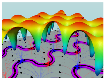
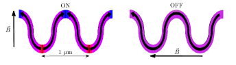
Planar permalloy (Ni80Fe20) nanowires exhibit a magnetic easy axis along their length. The wires we produce have an undulating shape which results in the magnetisation configuration having two distinct states, as shown in Figure 1. The ground or ‘off’ state contains a single continuous magnetic domain along the length of the wire. In this state there are nominally no out-of-plane fringing fields and thus no interaction with the atoms. A higher energy, metastable ‘on’ state is also possible, hosting many domains, situated at the wire apexes. This results in large fringing fields and hence a strong interaction. The nanowires can be forced into the ‘on’ state by application of an external in-plane magnetic field pulse, orthogonal to the length of the wire to saturate magnetisation in this direction. Relaxation after the pulse results in the magnetisation aligning to local wire edges, leading to a DW forming at each wire apex. The result is an extended periodic 2D array of eight million alternating north and south poles22 which constitutes a magnetic mirror which reflects atoms9. The ground state can then be recovered via the application of a magnetic field pulse along the length of the wire, causing pairwise annihilation of the DWs and leaving a continuous magnetisation.
A paramagnetic atom entering a magnetic field experiences a Zeeman interaction energy, , given by
| (1) |
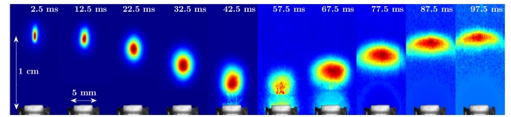
where is the atom’s magnetic quantum number, is the Landé g-factor and is the Bohr magneton. Thus a magnetic field gradient will result in the atom experiencing a Stern-Gerlach force, , given by . Atoms which have are ‘weak-field-seeking’ and are repelled from high magnetic fields. In our experiment a cloud of 87Rb atoms is laser-cooled at a height of 10 mm above the nanowire array in a magneto-optical trap, and is optically pumped to ensure that it is prepared in a weak-field-seeking () state. The cloud is then allowed to fall under gravity such that the atoms enter the fringing fields from the DWs and are subsequently reflected, observed in a series of fluorescence images shown in Figure 2. This clearly demonstrates the feasibility of manipulating ultracold atoms using DW fringing fields.
The atom dynamics during reflection are determined by the shape and magnitude of the fringing fields, which have been calculated. Such calculations show that extremely large magnetic field gradients are produced; within 10 nm of the surface these can reach T/m with corresponding field strengths of around 1 T. An atom dropped from a height of 10 mm will be reflected at heights of <500 nm. The field gradients in this region are sufficiently large that an atom approaching the nanowires effectively experiences a point interaction with the field. Thus it is possible to use the calculated fields to define an effective isosurface of from which the atoms can be considered to reflect specularly. This surface is a level set of the field (1.54 mT) for which the Zeeman interaction energy of a 87Rb atom in the specified magnetic sublevel is equal to the initial gravitational potential energy. This surface is illustrated above the nanowire array in Figure 1. An ideal magnetic mirror has a sinusoidally varying in-plane magnetisation9, which yields a flat equipotential surface. The 2D array of DWs mimics the general pattern of alternating magnetisation direction, but deviations from a pure sinusoidal form produce a roughness in , and hence a corrugated isosurface. The result is that a cloud of atoms entering the DW fringing fields will be reflected diffusely. This is shown in Figure 2 by the increased lateral extent of the cloud after reflection.
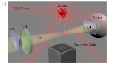
Quantitative analysis of the dynamics of the atoms is provided by the use of an intensity-stabilised light sheet, as illustrated in Figure 3. A resonant laser beam is focussed in one direction by cylindrical lenses, passing between the nanowire array and the initial location of the atomic cloud. As falling atoms pass through the light sheet they scatter photons, causing a dip in intensity. After the atoms have been reflected there is a second dip as they pass through again on the way back up. The light sheet has low intensity and is retroreflected to minimise any perturbation of the atoms. We estimate a sensitivity of around atoms with negligible heating of the cloud.
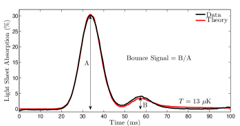
An example of the signal provided by the light sheet is shown in Figure 3(b). Also shown is the theoretical prediction made via Monte Carlo simulations of the atom cloud dynamics. We see excellent agreement between theory and data for a large range of parameters. The bounce signal is strongly dependent on initial temperature; if the cloud is too hot then the atoms spread out such that there are fewer atoms in the light sheet at any time, reducing the overall signal size, and the two peaks broaden such that it is no longer possible to resolve the bounce signal. For this reason, the remainder of the work was conducted at our minimum temperature of 10-15 K.
The ‘on’ and ‘off’ magnetic states of the nanowires (c.f. Figure 1(b)) are easily selected using single magnetic field pulses. Thus the fringing fields can be toggled, and the mirror switched on and off as the atom-field interaction is tuned. Investigation of this switching process was carried out via examination of the bounce signal, which represents a probe of the collective magnetic configuration. The resulting data are shown in Figure 4(a). We observe that the interaction can be toggled with 100% reliability. The pulses used to reconfigure the array have a minimum duration of around 0.5 ms, limited by the inductance of the coils, but in theory could be as short as a few ns, as the switching process occurs on an extremely short timescale23. Varying the size of the field used to switch the mirror permits analysis of the micromagnetic behaviour of the array, as the reflectivity of the device is directly correlated to the resulting bounce signal. Example data resulting from this process are shown in Figure 4(b).
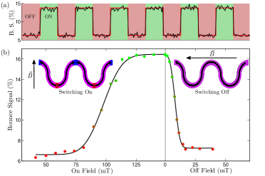
There is a gradual turning ‘on’ and ‘off’ of the chip, because the micromagnetic reconfiguration processes of populating and annihilating DWs occur over ranges of applied external field. The data are fit very well (reduced ) by error functions, which indicates that there is a normal distribution of required switching fields amongst the DW sites. This inherent variation indicates random fluctuations within the fabrication process and the stochastic nature of magnetic switching events. From the fits we extract a mean switching-on field, of 98.0 0.4 mT with a width, , of 15.8 0.8 mT. The mean switching-off field is 8.1 0.3 mT with a width of 4.6 0.4 mT. Measurements using the magneto-optical Kerr effect and scanning Hall probe microscopy are in good agreement with the fits in Figure 4. In normal operation fields significantly larger than the mean values are used to try and ensure switching of the entire array.
We have experimentally demonstrated the manipulation of ultracold atoms using DWs in magnetic nanowires, thus establishing the feasibility of creating atom chip devices based on reconfigurable nanomagnetic technology. Via a detailed examination of the interface between these two disparate regimes we have also shown that it is possible to use atom dynamics as a probe of nanomagnetic behaviour, which could lead to immediate applications. For example, experiments similar to the one we present could be used to probe artificial spin-ice arrays24 with different magnetic monopole configurations (and therefore fringing fields) but near-identical overall magnetisation. Work is also currently underway to exploit the inherently small lengthscale of the device to allow surface interactions to be studied at distances of less than 50 nm, c.f.25.
However, the most attractive feature of the approach exemplified by our proof-of-principle experiment is that it allows for the control of atomic motion via magnetic interactions that can be quickly, remotely and reliably tuned through the application of macroscopic magnetic fields. The intrinsic freedom afforded by the lithographic methods used to create planar nanowires, as well as the inherently mobile nature of the DWs, opens the door to a variety of devices. For example, DW fringing fields have already been utilised to confine macroscopic objects26, 27, and we plan to use them in an analogous manner as the basis for mobile atom traps17. A scheme for atom trapping based on such nanomagnetic technology would provide exceptional atomic confinement through extremely high trap frequencies and trapping volumes smaller than the de Broglie wavelength28. When combined with the controlled transport of DWs this will offer a dynamic architecture that lends itself well to future quantum information processing applications.
Methods Summary
Details of the design, manufacture and characterisation of the nanowire array can be found in 22. Theoretical calculations of the DW fringing fields were performed using a simple analytical model described in 29. The accuracy of the model was verified through comparison with proprietary code which solves the Landau-Lifshitz-Gilbert equation within a finite element/finite boundary framework 30. We observe errors less than 10% for distances above 100 nm from the nanowire surface. The effective isosurface is calculated from these fringing fields.
Predictions of the atom dynamics were provided by Monte Carlo simulations which propagate classical trajectories of non-interacting atoms. The distributions of atom position and velocity are initialised in accordance with experimental data. Repulsion from the fringing fields is treated as a classical reflection from the computed effective isosurface. The effects of the optical pumping and light sheet beams on the internal dynamics and motion of the atoms are included. The only free parameter is atom number.
We prepare the state of the nanowire array using a set of Helmholtz coils. Up to 200 A is passed through the coils by discharging car batteries. A rheostat allows a continuous range of magnetic fields to be selected. The ‘on’ coils are also used to realise the field for the magneto-optical trap (MOT). The MOT is loaded for 10 s followed by optical molasses, cooling the atoms to around K. The atoms are then optically pumped to the desired state. A quantisation axis is maintained by a magnetic field of 0.2 mT for the duration of the experiment. The atoms pass through a circularly polarised, retroreflected light sheet which is intensity-stabilised to better than 0.1%. The radii of the light sheet beam waist are 90 m and 3.9 mm. The signal from the light sheet is monitored using an amplified avalanche photodiode.
References
- 1 Wildermuth, S. et al. Bose-Einstein condensates: microscopic magnetic-field imaging. Nature 435, 440 (2005).
- 2 Gierling, M. et al. Cold-atom scanning probe microscopy. Nat. Nanotechnol. 6, 446-451 (2011).
- 3 Aoki, T. et al. Observation of strong coupling between one atom and a monolithic microresonator. Nature 443, 671 (2006).
- 4 Kohnen, M. et al. An array of integrated atom-photon junctions. Nature Photon. 5, 35-38 (2010).
- 5 Meystre, P. Atom Optics, Springer-Verlag, New York (2010).
- 6 Adams, C. S., Sigel, M., & Mlynek, J. Atom optics. Phys. Rep. 240, 143-210 (1994).
- 7 Reichel, J. & Vuletic, V. (ed.) Atom Chips, Weinheim, Wiley-VCH (2011).
- 8 Fortágh, J. & Zimmermann, C. Magnetic microtraps for ultracold atoms. Rev. Mod. Phys. 79, 235-289 (2007).
- 9 Hinds, E. A. & Hughes. I. G. Magnetic atom optics: mirrors, guides, traps, and chips for atoms. J. Phys. D 32, R119–R146 (1999).
- 10 Jones, M. P. A., Vale, C. J., Sahagun, D., Hall, B. V. & Hinds E. A. Spin coupling between cold atoms and the thermal fluctuations of a metal surface. Phys. Rev. Lett. 91, 080401 (2003).
- 11 Drndić, M., Johnson, K. S., Thywissen, J. H., Prentiss, M. & Westervelt, R. M. Micro-electromagnets for atom manipulation. Appl. Phys. Lett. 72, 2906-2908 (1998).
- 12 Lev, B., Lassailly, Y., Lee, C., Scherer, A. & Mabuchi, H. Appl. Phys. Lett. Atom mirror etched from a hard drive. 83, 395-397 (2003).
- 13 Wang, J. Y. et al. Perpendicularly magnetized, grooved GdTbFeCo microstructures for atom optics. J. Phys. D 38, 4015-4020 (2005).
- 14 Xing, Y. et al. Fabrication of magnetic atom chips based on FePt. J. Magn. Mag. Mat. 313, 192-197 (2007).
- 15 Whitlock, S., Gerritsma, R., Fernholz, T. & Spreeuw, R. J. C. Two-dimensional array of microtraps with atomic shift register on a chip. New J. Phys. 11, 023021 (2009).
- 16 Singh, M., Volk, M., Akulshin, A., Sidorov, A., McLean, R. & Hannaford, P. One-dimensional lattice of permanent magnetic microtraps for ultracold atoms. J. Phys. B 41, 065301 (2008).
- 17 Allwood, D. A., Schrefl, T., Hrkac, G., Hughes, I. G. & Adams, C. S. et al. Mobile atom traps using magnetic nanowires. Appl. Phys. Lett. 89, 014102 (2006).
- 18 Dean, J., Bryan, M. T., Schrefl, T. & Allwood, D. A. Stress-based control of magnetic nanowire domain walls in artificial multiferroic systems. J. Appl. Phys. 109, 023915 (2011).
- 19 Wolf, S. A. Spintronics: a spin-based electronics vision for the future. et al. Science 294 1488 (2001).
- 20 Allwood, D. A. Magnetic domain-wall logic. et al. Science 309, 1688 (2005).
- 21 Parkin, S. S. P., Hayashi, M. & Thomas, L. Magnetic Domain-Wall Racetrack Memory. Science 320, 190 (2008).
- 22 Hayward, T. J. et al. Design and characterization of a field-switchable nanomagnetic atom mirror. J. Appl. Phys. 108, 043906 (2010).
- 23 Atkinson, D. et al. Magnetic domain-wall dynamics in a submicrometre ferromagnetic structure. Nature Mat. 2, 85-87 (2003).
- 24 Ladak, S., Read, D. E., Perkins, G. K., Cohen, L. F., Branford, W. R. Direct observation of magnetic monopole defects in an artificial spin-ice system. Nature Phys. 6, 359-363 (2010).
- 25 Mohapatra, A. K. & Unnikrishnan, C. S. Measurement of the van der Waals force using reflection of cold atoms from magnetic thin-film atom mirrors. Europhys. Lett. 73, 839-845 (2006).
- 26 Ruan, G. et al. Simultaneous magnetic manipulation and fluorescent tracking of multiple individual hybrid nanostructures. Nano Lett. 10, 2220 (2010).
- 27 Bryan, M. T. et al. Switchable cell trapping using superparamagnetic beads. IEEE Magn. Lett. 1, 1500104 (2010).
- 28 Salem, R. et al. Nanowire atomchip traps for sub-micron atom surface distances. New J. Phys. 12, 023039 (2010).
- 29 West, A. D., Hayward, T. J., Weatherill, K. J., Schrefl, T., Allwood, D. A. & Hughes, I. G. A simple model for calculating magnetic nanowire domain wall fringing fields. Preprint at (2010).
- 30 Schrefl, T., Schabes, M. E., Suess, D. & Stehno, M. Dynamic micromagnetic write head fields during magnetic recording in granular media. IEEE Trans. Magn. 40, 2341 (2004).
AcknowledgementsThis work was supported financially by EPSRC grants EP/F025459/1 and EP/F024886/1.
Author ContributionsA.D.W., K.J.W., T.J.H., D.A.A. and I.G.H. contributed to the writing of the manuscript, the experiment was designed and built by A.D.W. and K.J.W., data analysis was carried out by A.D.W., K.J.W. and I.G.H., Monte Carlo simulations were performed by A.D.W., micromagnetic simulations were performed by T.J.H. and T.S., the magnetic nanostructures were designed by T.J.H., D.A.A., M.R.J.G. and T.S., fabrication and characterisation of the nanowires was carried out by T.J.H. and P.W.F., C.S.A. came up with the initial concept, D.A.A. and I.G.H. managed the project.
Author Information The authors declare no competing financial interests. Correspondence and requests for materials should be addressed to I.G.H. (i.g.hughes@durham.ac.uk).
Methods
The nanowires were fabricated using electron-beam lithography with liftoff processing. Metallisation was achieved by thermal evaporation. A 2 mm 2 mm area was written with nanowires of cross section 125 nm 30 nm. The wires are written with an undulating pattern of wavelength 1 m and adjacent wires are displaced by a distance of 1 m. All the wires extend across the full 2 mm of the written area.
Characterisation of the magnetisation reconfiguration processes of the wires was performed previously via magnetic hysteresis measurements using MOKE22. This gives a measurement of the collective reconfiguration of the magnetisation structure. Additional characterisation was also provided by SHP microscopy22 which provides imaging of individual DWs over a very small fraction of the chip.
Theoretical calculations of the resulting fringing fields created by the DWs were performed using a simple analytic model which we have developed29. In its most basic form, the DW is approximated as a point ‘magnetic charge’, , which has a size proportional to the wire’s cross-section. The magnetic flux density associated with this charge is then given by . Extending the model allows the DW to be represented as a 2D object, affording a more accurate calculation. The accuracy of this model was verified through comparison with calculations based on micromagnetically simulated magnetisation structures. This method utilises proprietary code to solve the Landau-Lifshitz-Gilbert equation within a finite element/finite boudnary framework30. The resulting fringing fields can be computed from the equivalent dipole charges at the surface of the nanowire. We observe excellent accuracy when using the analytic models with errors typically less than 10% for heights above 100 nm.
Tesselating the result from our analytic model yields the field from the domain wall array and hence allows for computation of the effective isosurface. The roughness of the isosurface can be characterised by the mean zenith angle, i.e. the angle between 0∘ and 90∘ quantifiying the deviation from a flat surface. This was calculated to be . Also of note is the fact that there are small regions between DWs where there is insufficient field to reflect the atoms; atoms impinging on these regions will either scatter stochastically from, or be adsorbed onto, the substrate.
Quantitative predictions of the atom dynamics are provided by Monte Carlo simulations which propagate classical trajectories of non-interacting atoms. The initial distributions of atom position and velocity are populated in accordance with experimental data. Repulsion from the fringing fields is treated as a classical reflection from the computed effective isosurface. The effects of the optical pumping and light sheet beams on the internal dynamics and motion of the atoms, and hence the resulting light sheet signal, are also included. The only free parameter in the simulations is atom number. Fitting this parameter is in fact a good method of measuring atom number as it is proportional to the integrated signal.
In our experimental procedure we initially prepare the configuration of the nanowire array by pulsing currents of up to around 200 A through Helmholtz coils in vacuum. The required current is provided by discharging a set of car batteries in series. Use of a rheostat allows a continuous range of fields to be selected. The ‘on’ coils are also used to realise the magneto-optical trap (MOT) which is loaded for 10 s and followed by a molasses ramp, cooling the atoms to around K. Modifying this molasses ramp reliably changes the resultant cloud temperature whilst maintaining a consistent experimental sequence. The atoms are then optically pumped for a duration of 2 ms, during which a quantisation axis parallel to the optical pumping and light sheet beams is defined via application of an external field of around 0.2 mT. This quantisation axis is kept on as the atoms fall in order to minimise any depolarisation of the atoms caused by the light sheet, and to ensure the adiabaticity of the atoms’ motion as they enter the large fringing fields. Optical pumping is achieved by addressing the transition with a laser beam with 0.6 W of power, and the transition with 40 W, both beams have a radius of 1.4 mm. The atoms pass through the retroreflected light sheet which is intensity-stabilised with a power of 50 nW. The radii of the semi-major axes of the light sheet’s profile are 90 m and 3.9 mm. Both the optical pumping beams and the light sheet beam are circularly polarised by a single quarter-wave plate. The light level is monitored using a Hamamatsu C5460 APD module.