Using physical insights and advanced first-principles calculations, we suggest that corundum (-Al2O3) is an ideal gate dielectric material for graphene transistors. Clean interface exists between graphene and Al-terminated (or hydroxylated) Al2O3 and the valence band offsets for these systems are large enough to create injection barrier. Remarkably, a band gap of 180 meV can be induced in graphene layer adsorbed on Al-terminated surface with an electron effective mass of 8 10-3 me, which could realize large ON/OFF ratio and high carrier mobility in graphene transistors without additional band gap engineering and significant reduction of transport properties. Moreover, the band gaps of graphene/Al2O3 system could be tuned by an external electric field for practical applications.
Theoretical Study of Corundum as an Ideal Gate Dielectric Material for Graphene Transistors
pacs:
73.22.-f, 68.65.Pq, 68.43.Bc, 68.47.GhGraphene has been studied intensively due to its unique electronic and mechanical properties such as extremely high carrier mobility (over 200000 cm2/Vs for suspended samples)Geim-Castro Neto . However, to utilize graphene, which has a zero band gap when it is pure, for electronic devices such as the field-effect transistors (FETs), it is essential to open up a band gap in graphene to realize the ON/OFF switch function. One way to open the band gap in graphene is utilizing the quantum confinement effect, e.g., etching graphene into one-dimensional nanoribbonsQimin-2007 ; M. Y. Han-2007 ; X. Li-2008 ; Wang-2008 . In practice, very narrow graphene nanoribbons (GNRs) ( 10 nm) are necessary to achieve a band gap of 0.2 eV (ON/OFF ratio 102)Qimin-2007 ; M. Y. Han-2007 ; X. Li-2008 ; Wang-2008 , but a large scale production of such narrow GNRs is still quite challenging. Moreover, the carrier mobility of GNRs (about hundreds of cm2/VsX. Li-2008 ; Wang-2008 ) is several magnitudes lower than that of graphene sheet due to the (intrinsic) band folding and phonon scatteringA. Betti-2011 as well as (extrinsic) difficulty in controlling the edge quality in experimentsX. Li-2008 ; Wang-2008 . Another way to open a band gap in graphene is breaking the inversion symmetry of the A, B sublattices, e.g., by placing graphene onto some special substrate. In this case, the band structure near the Dirac point or the carrier mobility of the graphene is better preserved if the interaction between graphene and substrates is weak. Obviously, this approach has technological advantages over the etching of graphene. However, a simple guideline on how to search an ideal substrate that could induce a sufficiently large band gap in graphene is still unclear, especially for substrate which can be integrated directly into the current FET technology.
Most of the graphene FETs to date employ silicon oxide (SiO2) as the bottom-gate dielectric and an alternative high-dielectric-constant (high-k) material as the top-gate dielectric (e.g., the amorphous structures of HfO2Zou-2010 and Al2O3Liao-Kim ). The integration of a high-k top-gate can push the FET performance to a much higher limit because it can better screen charged impurities and enhance carrier mobility in grapheneC. Jang-2008 ; Liao-Kim ; Zou-2010 . Analogy to silicon FET, an optimal high-k gate dielectric material should have high dielectric constant, large injection barrier (i.e., large band offset ( eV) with respect to graphene), high chemical stability, and no or minimal interface states at the high-k-oxide/graphene interfaceXiang-2009 . In addition, an ideal high-k dielectric is desired to have the ability to open an adequate gap in graphene for FET operation.
Although several calculations have shown that a small gap could be induced in graphene by SiO2Y. Kang-2008 ; N. T. Cuong-2011 , HfO2K. Kamiya-2011 , or BNG. Giovannetti-2007 substrates, a general rule to find a substrate which can induce a larger band gap in graphene is still lacked. Here, we propose that one should search for the substrate which has atoms with large chemical potential difference at the surface and is commensurate with the graphene lattice. These two conditions can cause large potential difference at the A, B sublattices of graphene, thus produce large band gap in graphene. Under this physical insight, we suggest that the (reconstructed) Al-terminated -Al2O3 (0001) surface is an ideal high-k-oxide substrate for graphene FETs. This is because after the reconstruction both Al and O are present at the surface and the chemical potential difference between Al and O is much larger than that of other popular substrates such as SiO2, BN, and HfO2 studied before, and the lattice mismatch between -Al2O3 (0001) and graphene is also relatively small. Carried out by advanced first-principles calculations, we demonstrate that a large band gap of 180 meV at the Dirac point appears in graphene layer adsorbed on Al-terminated (0001) surface with a quite small effective mass of 8 10-3 me for Dirac fermions. As we expected, the band gap of graphene on Al2O3 is significantly larger than on other widely used substratesnote1-LDA . The size of the band gaps of graphene/Al2O3 systems could be further tuned by an external electric field for practical applications. Moreover, interface states can be eliminated if graphene is grown on Al-terminated (or hydroxylated) Al2O3 (0001) surface and the valence band offsets for these hybrid systems are large enough for injection barrier.
All the density-functional-theory (DFT) calculations are performed by using the VASP codeVASP . Projector augmented wave (PAW) potentials are used to describe the core electrons, and generalized gradient approximation (GGA) with the PBE functional is selected in our calculations. We find that the van de Waals (vdW) interaction plays an indispensable role in accurately determining the adsorption configuration and binding strength in this system. The effect of vdW interactions is taken into account by using the empirical correction scheme of Grimme (DFT + D/PBE)vdW , which has been proved to be successful in describing the geometries of graphene related structuresG. Mercurio-D. Stradi . Our DFT+D/PBE calculations show that the interlayer distance of graphite is 3.22 Å and the interlayer binding energy is -54 meV/C-atom, in excellent agreement with quantum Monte Carlo calculation (-56 meV/C-atom)L. Spanu-2009 and experimental value (-525 meV/C-atom)R. Zacharia-2004 . It is well-known that GGA type calculations usually underestimate the band gaps of semiconductors and the absolute band edge energy from the GGA calculation is not always reliable. Since hybrid functional calculations could give improved results for both conventional semiconductorsA. Alkauskas-2008 and graphene nanostructuresV. Barone-2006 , we adopt HSE hybrid functional to calculate the electronic structures of these Al2O3/graphene systems. The Al2O3 (0001) surface is modeled by a slab containing six oxygen O3 layers and twelve or eleven aluminum layers (depending on the specific surface studied). The second surface of the slab is passivated by pseudo H atoms and a 15 Å-vacuum region is included. Single-layer or bilayer graphene with 2 2 periodicity is placed on 1 1 cell of Al2O3 with a lattice mismatch 2%strain-effect . A -centered 24 24 1 k-point sampling is used for the Brillouin-zone integration. The energy cutoff is set to 400 eV and structural optimization is carried out on all systems until the residual forces are converged to 0.01 eV/Å. The dipolar correction has been includedNeugebauer-1992 .
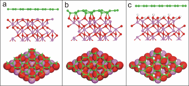
-Al2O3 has rhombohedral symmetry Rc (, No. 167). The oxygen atoms form a nearly hcp structure, and the metal atoms fill two-thirds of the octahedral sites between the oxygen layersHenrich-1994 . The (0001) surface of -Al2O3 is of major technology importance because it is often used as a substrate in growth of semiconducting as well as superconducting materials. Low-energy electron diffraction (LEED) revealed that the (0001) crystal surface exhibits a 1 1 structure below 1250∘ in air or in vacuumHenrich-1994 ; G. Renaud-1998 ; J. Toofan-1998 . Although theoretical calculations demonstrated that Al-terminated (0001) surface is the most stable oneFelice-1999 ; Wang-2000 , both Al- and O- terminated (0001) surfaces are observed in experiments and considered in our present workHenrich-1994 ; G. Renaud-1998 ; J. Toofan-1998 .
For the Al-terminated (0001) surface, our calculations show that the topmost Al atoms move down 0.65 Å into the next oxygen layer after the relaxation compared to the cleaved surface, as shown in Fig. 1a. This surface reconstruction stabilizes the surface by the large suppression of surface polarizationFelice-1999 ; Wang-2000 . In order to investigate the stable interface structures, we have calculated all the high symmetrical arrangements between graphene and Al-terminated surface, where a surface Al or O atom is directly below either: a graphene C atom (TAl or TO), the hollow site of graphene C atoms (HAl or HO), or the center of C-C bridge site (BAl or BO). In addition, the case of a C atom directly above the center of surface Al-O bridge site is also considered. Our DFT+D/PBE total energy calculations indicate that the most stable configuration is the TAl (Fig. 1a) with an adsorption energy of -76.4 meV/C-atom and the distance between graphene layer and substrate surface is 2.74 Å. The adsorption energy of the TAl configuration is more negative than other high symmetrical configurations by 2 9 meV/C-atom. It should be noticed that the vdW correction is very important in this case: without the vdW correction, the calculated interface distance of the TAl configuration would be drastically increased to 3.31 Å and the adsorption energy would be only -2.6 meV/C-atom; the energy difference between TAl and other configurations is within 2 meV/C-atom in the absence of vdW correction. LDA calculation could give a similar interlayer distance between graphene and substrate surface, but the binding energy is still largely underestimated by 34 meV/C-atom.
On the O-terminated surface, as each O atom has one dangling bond, the O-terminated surface is chemically reactive and could strongly interact with the graphene layerL. Han-2010 . For the lowest energy configuration, all three surface O atoms in the unit cell form chemical bonds with the graphene layer to suppress the surface dangling bonds, as shown in Fig. 1b. The C-O bond length ranges from 1.45 to 1.50 Å. These C-O binding severely distort the planar graphene structure (C-C bond length varies from 1.36 to 1.49 Å) and the binding energy between graphene and O-terminated surface is -349 meV/C-atom, which is much larger than that of Al-terminated surface. In addition, fully hydroxylated Al2O3 surface is also considered, as H atoms can be incorporated into the bulk structure during growthHenrich-1994 . Previous calculations also demonstrated that the stability of fully hydroxylated surface is comparable to the Al-terminated one and much more stable than O-terminated surfaceFelice-1999 ; Wang-2000 . Similar to Al-terminated surface, graphene layer adsorbed on hydroxylated surface also belongs to vdW interaction. The most stable configuration is BO (one surface O directly below the center of C-C bridge site), as shown in Fig. 1c. The interlayer distance between graphene layer and hydroxylated surface ranges from 2.31 Å to 3.18 Å due to the rippled structure at the interface and the binding energy is -49.2 meV/C-atom, slightly smaller than the binding strength of interlayers in graphite. The binding energy of BO case is slightly lower than that of TO and HO within 1 meV/C-atom, indicating that these configurations are almost degenerate in energy.
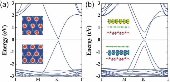
After knowing the stable interface structures, we turn to understand the effects of Al2O3 substrate on the electronic property of graphene. The HSE band structure of single-layer graphene adsorbed on Al-terminated surface (TAl configuration) is shown in Fig. 2a. Notably, the degeneracy of Dirac cone of graphene is lifted and a band gap of 182 meV (69 meV in DFT+D/PBE calculations) appears at the Fermi level, generating an effective mass of the Dirac fermions 8 10-3 me. This is because the inversion symmetry in the graphene plane is broken on Al2O3 surface so the A, B sublattices, which is equivalent in free-standing graphene, is no longer equivalent. We find that the electrostatic potential difference of graphene C atoms at the A and B site differ by 165 meV, close to the value of the band gap. The charge density distributions of conduction band minimum (CBM) and valence band maximum (VBM) (inset of Fig. 2a) are found separately located in the different A and B sublattices of graphene layer, which is consistent with our explanation.
The sizes of band gaps of graphene in other high symmetrical configurations are close to that of TAl, indicating that a similar ON/OFF ratio could be obtained even if graphene slides away from its ground state TAl configuration. Remarkably, the band gap of graphene on Al-terminated Al2O3 is comparable to 10-nm-width GNRs in experimentsWang-2008 ; M. Y. Han-2007 ; X. Li-2008 . Meanwhile, the effective mass of carriers in graphene/Al2O3 is an order lower than that of GNRs ( 0.07 me) from theoretical calculationM. Long-2009 , strongly indicating the much higher carrier mobility of graphene/Al2O3 in practice. The band alignment between the graphene and substrate surface is found to be type-I and there are no interface states around Fermi level for the Al-terminated interface (Fig. 2a). By distinguishing the respective graphene and Al2O3 states, we can calculate the band offset for this hybrid system. The valence band offset between graphene and Al2O3 is about 2.35 eV from the hybrid functional calculation (DFT+D/PBE level calculation seriously underestimates the valence band offset by 1 eV), comparable to that of silicon and Al2O3Xiang-2009 , which is high enough for injection barrier.
The electronic properties of bilayer graphene on Al-terminated surface, as shown in Fig. 2b. The equilibrium graphene interlayer distance with AB stacking is 3.18 Å. Similar to single-layer graphene, a band gap of 138 meV is induced in bilayer graphene due to the inversion symmetry breaking. The VBM and CBM are contributed by A1 and B2 sublattices (A1 and B1 belong to the bottom layer while A2 and B2 belong to the top layer) in different graphene layers, respectively, as shown in Fig. 2b. The valence band offset between bilayer graphene and Al2O3 is 2.26 eV, slightly smaller than that of single-layer graphene. It is important to notice that the band gaps of single-layer or bilayer graphene on Al-terminated surface are large enough to create sufficient ON/OFF ratio in FET applicationsQimin-2007 ; M. Y. Han-2007 ; X. Li-2008 ; Wang-2008 . As we expected, the band gap of graphene on Al2O3 is significantly larger than that on other popular substrates such as SiO2, HfO2, and BN, indicating that -Al2O3 is a better choice for gate materialnote1-LDA .
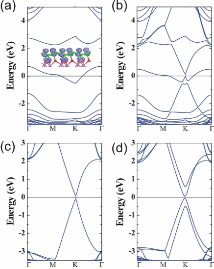
The electronic properties of graphene on O-terminated surface are completely different from that of Al-terminated one. Due to the strong interaction between graphene and surface O atoms, the linear band characteristic of graphene disappears, as shown in Fig. 3a. The gap states in Fig. 3a originate from the hybridization between graphene C orbitals and surface O orbitals, shown as the inset in Fig. 3a. When a second graphene layer is placed on the surface (the graphene interlayer distance varies from 3.09 Å to 3.75 Å due to the rippled structure of the bottom layer), these gap states couple with the second layer graphene states and perturb its linear band distribution, as shown in Fig. 3b. A band gap of 140 meV appears for the second graphene layer, but the interface states exist inside the gap. Because these localized interface states can largely suppress the high mobility of graphene, O-terminated surface must be avoided to contact with graphene when gating graphene in experiments.
The electronic properties of graphene adsorbed on hydroxylated surface show similar behaviors to the Al-terminated surface, as shown in Figs. 3c and 3d for BO configuration. No interface states around Fermi level are found and a band gap of 84 meV is induced in graphene layer with the effective mass of 4 10-3 me for the Dirac fermion. The valence band offset between graphene and hydroxylated surface is 3.39 eV, larger than that of Al-terminated one. Moreover, the electronic properties of TO and HO configurations are quite similar to that of BO. Comparing to the single layer case, the bilayer graphene on the hydroxylated surface has a larger band gap of 126 meV and smaller band offset of 3.24 eV, as shown in Fig. 3d. Clearly, O-terminated surface should be hydroxylated in order to make clean interface between graphene and Al2O3. Although the amorphous structure of Al2O3 has been selected as a top gate in some experimentsLiao-Kim , it is difficult for us to directly compare our results with these experiments due to the different phases.
Finally, we considered the electronic properties of graphene/Al2O3 hybrid system under an external electric field () to simulate the gating effect in experimentsNeugebauer-1992 . Taking graphene on Al-terminated surface as examples, Fig. 4 shows the band gap and valence band offset of graphene/Al2O3 system as a function of . For single-layer graphene on Al2O3, a negative increases the band gap while the trend is opposite for a positive , as shown in Fig. 4a. This is because a positive (negative) increases (decreases) the distance between graphene and surface, e.g., the distance increases (decreases) from 2.74 Å to 2.86 (2.69) Å when = 0.6 (-0.6) V/Å. The increase of the distance between graphene and substrate reduces the potential difference , thus changing the band gap. The variation of potential difference also influences the valence band offset, as shown in Fig. 4. The valence band offset increases (decreases) with a negative (positive) and varies from 2.49 eV to 2.05 eV under -0.6 eV/Å 0.6 eV/Å.
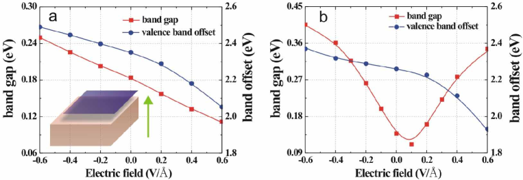
The situation is quite different for bilayer graphene/Al2O3 (Fig. 4b) under an . Due to the symmetry, the band gap of bilayer graphene is determined mainly by the absolute difference of .Y. Zhang-2009 This value reaches minimum at V/Å when the system has a minimum anticrossing band gap around 112 meV. As increases or decreases from this value, increases, which makes the band gap increases as well, as shown in Fig. 4b. For example, the band gap of bilayer graphene increases to 361 meV at = -0.4 V/Å. The valence band offset changes between 2.37 eV and 1.93 eV for -0.6 eV/Å 0.6 eV/Å. Thus, even under high , the valence band offset (injection barrier) of graphene/Al2O3 is still large enough.
with physical insights and by first-principles calculations we demonstrate that -Al2O3 is an ideal high-k gate material for graphene FETs. There are no interface states between graphene and Al-terminated or hydroxylated Al2O3 surface and the valence band offset for this hybrid system is larger than 2 eV. Remarkably, a band gap of 180 meV appears in graphene layer deposited on Al-terminated surface, which is significantly larger than on other popular used substrates. Furthermore, the band gap of graphene/Al2O3 system could be tuned by an external electric field for practice applications.
The authors thank the helpful discussion with Prof. Jaejun Yu (SNU). The work at NREL was supported by the U.S. Department of Energy under Contract No. DE-AC36-08GO28308.
References
- (1) A. K. Geim and K. S. Novoselov, Nature Mater. 6, 183 (2007); A. H. Castro Neto, F. Guinea, N. M. R. Peres, K. S. Novoselov, and A. K. Geim, Rev. Mod. Phys. 81, 109 (2009).
- (2) Q. Yan, B. Huang, J. Yu, F. Zheng, J. Zhang, J. Wu, B. -L. Gu, F. Liu, and W. H. Duan, Nano Lett. 7, 1469 (2007).
- (3) M. Y. Han, B. Ozyilmaz, Y. Zhang, and P. Kim, Phys. Rev. Lett. 98, 206805 (2007).
- (4) X. Li, X. Wang, L. Zhang, S. Lee, and H. Dai, Science 319, 1229 (2008).
- (5) X. Wang, Y. Ouyang, X. Li, H. Wang, J. Guo, and H. Dai, Phys. Rev. Lett. 100, 206803 (2008).
- (6) A. Betti, G. Fiori, and G. Iannaccone, Appl. Phys. Lett. 98, 212111 (2011).
- (7) K. Zou, X. Hong, D. Keefer, and J. Zhu, Phys. Rev. Lett. 105, 126601 (2010).
- (8) L. Liao, J. Bai, Y. Qu, Y. Huang, and X. Duan, Nanotechnology 21, 015705 (2010); S. Kim, J. Nah, I. Jo, D. Shahrjerdi, L. Colombo, Z. Yao, E. Tutuc, and S. K. Banerjee, Appl. Phys. Lett. 94, 062107 (2009).
- (9) C. Jang, S. Adam, J.-H. Chen, E. D. Williams, S. Das Sarma, and M. S. Fuhrer, Phys. Rev. Lett. 101, 146805 (2008).
- (10) H. J. Xiang, L. F. Da Silva, H. M. Branz, and S. -H. Wei, Phys. Rev. Lett. 103, 116101 (2009).
- (11) Y. Kang, J. Kang, and K. J. Chang, Phys. Rev. B 78, 115404 (2008).
- (12) N. T. Cuong, M. Otani, and S. Okada, Phys. Rev. Lett. 106, 106801 (2011).
- (13) K. Kamiya, N. Umezawa, and S. Okada, Phys. Rev. B 83, 153413 (2011).
- (14) G. Giovannetti, P. A. Khomyakov, G. Brocks, P. J. Kelly, and J. van den Brink, Phys. Rev. B 76, 073103 (2007).
- (15) The LDA band gap of graphene on Al2O3 is 178%, 480%, and 144% larger than on SiO2N. T. Cuong-2011 , HfO2K. Kamiya-2011 and BNG. Giovannetti-2007 , respectively.
- (16) G. Kresse and J. Furthmüller, Comput. Mater. Sci. 6, 15 (1996).
- (17) S. Grimme, J. Comput. Chem. 27, 1787 (2006).
- (18) G. Mercurio, E. R. McNellis, I. Martin, S. Hagen, F. Leyssner, S. Soubatch, J. Meyer, M. Wolf, P. Tegeder, F. S. Tautz, and K. Reuter, Phys. Rev. Lett. 104, 036102 (2010); D. Stradi, S. Barja, C. Diaz, M. Garnica, B. Borca, J. J. Hinarejos, D. Sanchez-Portal, M. Alcami, A. Arnau, A. L. Vazquez de Parga, R. Miranda, and F. Martin, Phys. Rev. Lett. 106, 186102 (2011).
- (19) L. Spanu, S. Sorella, and G. Galli, Phys. Rev. Lett. 103, 196401 (2009).
- (20) R. Zacharia, H. Ulbricht, and T. Hertel Phys. Rev. B 69, 155406 (2004).
- (21) A. Alkauskas, P. Broqvist, F. Devynck, and A. Pasquarello, Phys. Rev. Lett. 101, 106802 (2008).
- (22) V. Barone, O. Hod, and G. E. Scuseria, Nano Lett. 6, 2748 (2006).
- (23) A strain of 2% does not influence the intrinsic electronic property of graphene, as shown in S. Choi, S. Jhi, and Y. -W. Son, Phys. Rev. B 81, 081407 (2010).
- (24) J. Neugebauer and M. Scheffler, Phys. Rev. B 46, 16067 (1992).
- (25) V. E. Henrich and P. A. Cox, The Surface Science of Metal Oxides (Cambridge University Press, Cambridge, England, 1994).
- (26) G. Renaud, Surf. Sci. Rep. 32, 1 (1998).
- (27) J. Toofan and P. R. Watson, Surf. Sci. 401, 162 (1998).
- (28) R. D. Felice and J. E. Northrup, Phys. Rev. B 60, 16287(R) (1999).
- (29) X. Wang, A. Chaka, and M. Scheffler, Phys. Rev. Lett. 84, 3650 (2000).
- (30) H. Liu, Q. Sun, L. Chen, Y. Xu, S. Ding, W. Zhang, and S. Zhang, Chin. Phys. Lett. 27, 077201 (2010).
- (31) M. Long, L. Tang, D. Wang, L. Wang, and Z. Shuai, J. Am. Chem. Soc. 131, 17728 (2009).
- (32) Y. Zhang, T. Tang, C. Girit, Z. Hao, M. C. Martin, A. Zettl, M. F. Crommie, Y. R. Shen, and F. Wang, Nature (London) 459, 820 (2009).