Corresponding author: S. Burger
URL: http://www.zib.de
URL: http://www.jcmwave.com
Email: burger@zib.de
Investigation of 3D Patterns on EUV Masks by Means of Scatterometry and Comparison to Numerical Simulations
Abstract
EUV scatterometry is performed on 3D patterns on EUV lithography masks. Numerical simulations of the experimental setup are performed using a rigorous Maxwell solver. Mask geometry is determined by minimizing the difference between experimental results and numerical results for varied geometrical input parameters for the simulations.
keywords:
EUV scatterometry, optical metrology, 3D rigorous electromagnetic field simulations, computational lithography, finite-element methodsThis paper will be published in Proc. SPIE Vol. 8166 (2011) 81661Q (Photomask Technology 2011; W. Maurer, F.E. Abboud, Editors, DOI: 10.1117/12.896839), and is made available as an electronic preprint with permission of SPIE. One print or electronic copy may be made for personal use only. Systematic or multiple reproduction, distribution to multiple locations via electronic or other means, duplication of any material in this paper for a fee or for commercial purposes, or modification of the content of the paper are prohibited.
1 Introduction
Extreme ultraviolet (EUV) lithography at a wavelength of about 13 nm is expected to replace deep ultraviolet (DUV) lithography for fabrication of integrated circuits with minimum feature sizes (critical dimension, ) as small as 22 nm or below. With decreasing feature sizes tolerance budgets of mask pattern dimensions get tighter. Metrology of such structures has to be performed for characterization and process control.
In previous works it has been shown that EUV scatterometry is a fast and robust method for characterizing masks with 1D-periodic patterns (line masks) [1, 2, 3, 4]. In this contribution we extend our research to the characterization of 2D-periodic patterns (array of contact holes).
In our method we compare the distribution of EUV light scattered off the sample to results from numerical simulations of the setup with different sets of geometrical parameters. Mask geometry is then determined by optimizing geometrical input parameters of the numerical simulations such that differences between measurement and simulation are minimized.
2 Experimental EUV scatterometry results
The data presented here were measured at the EUV reflectometry facility of PTB [5, 6] in its laboratory at the storage ring BESSY II. The PTB’s soft X-ray radiometry beamline [7] uses a plane grating monochromator which covers the spectral range from 0.7 nm to 35 nm and which was particularly designed to provide highly collimated radiation. For this purpose it uses a long focal length of 8 m in the monochromator, and the focusing in the non-dispersive direction is provided by a collecting pre-mirror with a focal length of 17 m. We achieve a collimation of the radiation in the experimental station to better than 200 rad and the scatter halo of the beam can be suppressed to below relative intensity at an angle of only 1.7 mrad to the central beam.
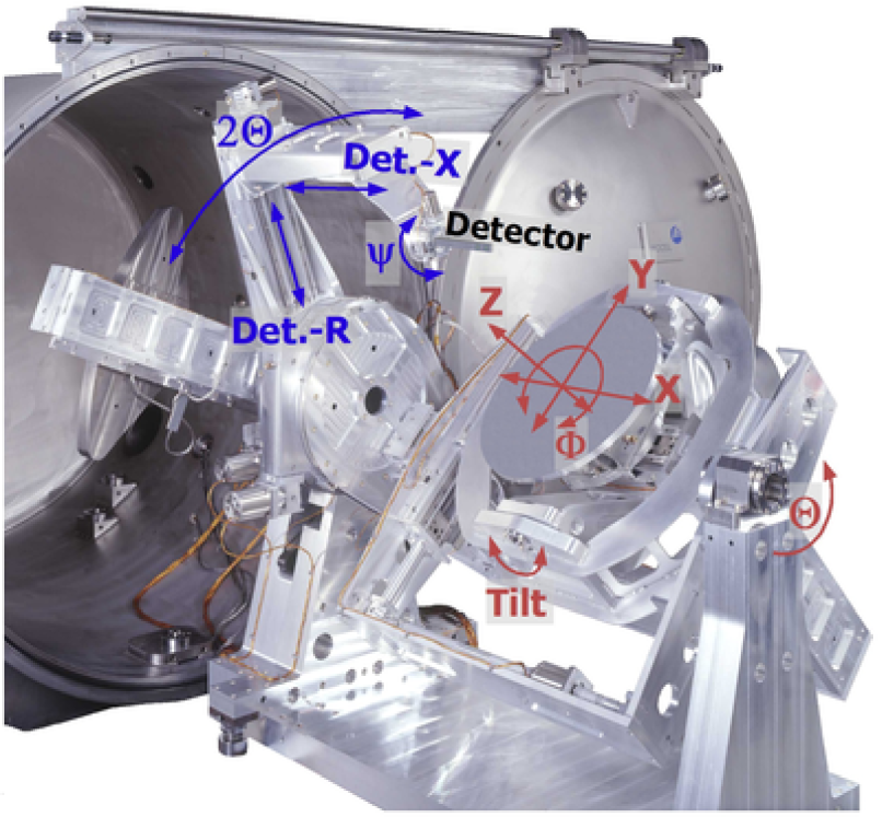
The measurement scheme for angular resolved scatterometry of periodic structures is presented in Figure 1 (left). Usually, the sample is set at a fixed angle to the incoming radiation and the detector is moved. Figure 1 (right) shows a photograph of the experimental setup: The probed photomask is mounted at the center of the (red marked) ---coordinate system. It is rotated such that the periodicity vectors of the periodic patterns on the mask are in - and -directions. The EUV probe beam is incident in the --plane. The detector can be freely moved to capture reflected - and -diffraction orders.
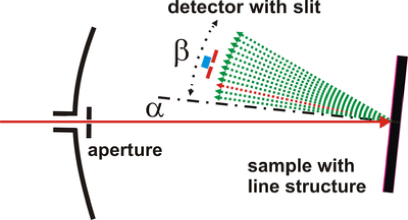
The presented experimental data are obtained from periodically structured areas on an EUV photomask. The structure for the measurements was a 1.4 mm by 1.4 mm large field with a 2D structure of quadratic contact holes with nominal 300 nm CD at 600 nm pitch in - and -direction. The measurement method used was angular resolved scatterometry. The scan range of the detector angle was from to , see Figure 1. The to diffraction orders were measured in -direction with respect to the sample using the movement of the detector in the plane of specular reflection. For the measurement of diffraction in the out-of-plane direction, the perpendicular movement of the detector was used [5]. Thus we also measured from the to order in -direction. As the EUV radiation is resonant with the underlying multilayer reflective coating, the measured diffraction intensities strongly depend on the actual wavelength. We measured at centre wavelength of the resonance peak of 13.54 nm, see Figure 3. Figure 2 shows a scatterogram for a measurement of the contact hole array in two different graphical representations.
3 Mask model and simulation method
3.1 Multilayer model
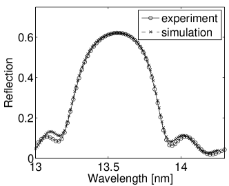
For characterizing the multilayer stack we have performed measurements of reflectivity off the blank multilayer mirror as a function of incident wavelength in a spectral range from 13 nm to 14.3 nm. The multilayer stack consists of 40 -multi-layers of molybdenum (Mo) and silicon (Si). It further contains a silicon capping layer, finished with a thin oxide layer, and it is placed on a SiO2 substrate. To model the -multi-layers we have chosen a four-layer stack consisting of a Mo-layer, a MoSi2-layer (interlayer), a Si-layer, and a second MoSi2-layer. A schematic is shown in Figure 4 (left). We have fitted the layer thicknesses of the blank mirror using the IMD multilayer programme [8], using also the therein provided material definitions. The resulting reflectivity spectrum is display in Figure 3 together with measured data. The obtained layer thicknesses are shown in Table 1. These values are used in the subsequent 3D simulations. For the thicknesses of the absorber stack (buffer, absorber and anti-reflection, ARC, layers) we have chosen the nominal values of the EUV mask (see Table 1).
| material | height | |||
|---|---|---|---|---|
| vacuum | 1 | 0 | ||
| ARC | nm | 0.9474 | 0.0316 | nm |
| absorber | nm | 0.9255 | 0.0439 | |
| buffer | nm | 0.9735 | 0.0131 | |
| oxide | nm | 0.9735 | 0.0131 | |
| capping | nm | 1.0097 | 0.0013 | |
| multi-layer (interlayer) | nm | 0.9681 | 0.0044 | 40 layers |
| multi-layer (Mo) | nm | 0.9206 | 0.0065 | 40 layers |
| multi-layer (interlayer) | nm | 0.9681 | 0.0044 | 40 layers |
| multi-layer (Si) | nm | 1.0097 | 0.0013 | 40 layers |
| substrate | 0.9735 | 0.0131 | ||
| lateral dimensions | 300 nm | |||
| (nominal) | 300 nm | |||
| 600 nm | ||||
| 600 nm | ||||
| 0 nm | ||||
| sidewall angle | 90 deg | |||
| illumination | angle of incidence | 6 deg | ||
| wavelength | 13.54 nm | |||
| polarization | ||||
3.2 Lateral layout: array of contact holes
The investigated mask holds several different patterns. Here we concentrate on analysis of a single of these patterns: an array of contact holes, Figure 4 (right) shows a schematic of the lateral layout. A pattern with a pitch of nm is investigated. Nominal values for the (bottom) CD’s are nm. We assume a sidewall angle of the absorber stack, , and a constant (vertical) corner rounding of the stack, . Free parameters in our investigation are the contact hole critical dimensions , , the sidewall angle , and the lateral corner rounding radius, .
3.3 Simulation setup
For rigorous simulations of the scattered EUV light field we use the finite-element (FEM) Maxwell solver JCMsuite. This solver incorporates higher-order edge-elements, self-adaptive meshing, and fast solution algorithms for solving time-harmonic Maxwell’s equations. Previously the solver has been used in scatterometric investigations of EUV line masks (1D-periodic patterns) [9, 3]. Recently we have reported on rigorous electromagnetic field simulations of 2D-periodic arrays of absorber structures on EUV masks [10]. This report contained a convergence study which demonstrates that highly accurate, rigorous results can be attained even for the relatively large 3D computational domains which are typically present in 3D EUV setups.
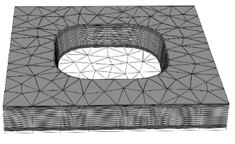
Briefly, the simulations are performed as follows: a scripting language (Matlab) automatically iterates the input parameter sets (, , , ). For each set, a prismatoidal 3D mesh is created automatically by the built-in mesh generator. Then, the solver is started, postprocessing is performed to extract the diffraction order efficiencies, and results are evaluated and saved. Figure 5 shows a graphical representation of a 3D mesh. As numerical settings for the solver, finite elements of fourth-order polynomial degree, automatic settings for the transparent boundary conditions, and a rigorous domain-decomposition method (to separate the computation of the light field in the multi-stack mirror from the computation in the structured absorber region) are chosen. Together with a relatively coarse lateral spatial discretization and a fine spatial discretization in -direction this setting yields discrete problems with between one and two millions of unknowns. These problems are solved by direct LU factorization on a computer with extended RAM memory (about 40 GB) and several multi-core CPU’s (total of 16 cores), with typical computation times of about 30 minutes (per parameter set). From comparison to a detailed convergence study on 3D EUV simulations [10] we estimate that we achieve relative accuracies better than 1 % for all diffraction orders with intensities greater than (relative to the intensity of the incoming beam).
4 Reconstruction of geometry parameters
4.1 Simulation results
The simulated scatterogram of the EUV mask pattern, where all parameters are set to nominal values, is shown in Figure 6. The left part of the Figure shows the diffraction intensities on a logarithmic, pseudo-color scale. The right part of the Figure displays the same simulation results in a 2D graph, together with results from the measurement. Only results with measured relative intensities larger than are displayed (cf., dashed line in Figure 2).
Each simulated diffraction order intensity, , is attributed a relative deviation:
where is the measured value and and denote the index of the diffraction order in -, resp., -direction.
A cost function, is attributed to the simulation parameters by summing over all diffraction orders , , with , where is the intensity of the illuminating plane wave:
Here, denotes the number of diffraction orders taken into account, and the zero diffraction order is omitted.
4.2 Reconstruction results
We have performed a series of simulations with varied parameter sets (, , , ), recorded the corresponding diffraction patterns and computed the corresponding cost functions / deviations . Figure 7 (left, center) shows how the cost function varies with and , in the investigated parameter ranges. We find the lowest cost function, i.e., the best correlation between experiment and simulation for the parameter set nm, nm, deg, nm. The measured and simulated diffraction spectra for this parameter set are displayed in Figure 7 (right). The agreement of most diffraction orders intensities is very good. We expect that the parameter values obtained with this scatterometric method are close to the real parameter values.
However, the fact that the differences between measurement and simulation are larger than both, expected experimental measurement
uncertainty and numerical errors, suggests the following advancements:
(i) More free parameters to be considered in the model (e.g., layer thicknesses ).
(ii) Larger parameter ranges to be scanned to avoid possibilities of optimizing to a local minimum.
(iii) A more refined geometrical model to take into account effects of
edge roughness [11, 12],
surface roughness, corner rounding at the
bottom corners, etc.
(iv) Reconstruction results to be validated by comparison to results obtained with other
measurement methods, like scanning electron microscopy (SEM) or atomic force microscopy (AFM).
Currently, computation times for the 3D simulations on large computational domains limit the applicability when many free parameters are taken into account (unless large computational power is available). For real-time reconstruction of using the same methods we plan to apply the reduced-basis method (RBM) which allows to decrease computation times for rigorous simulations of parameterized simulation setups by several orders of magnitude [13, 14].
5 Conclusion
Scatterometric measurements of 2D periodic patterns on EUV masks have been performed using the X-ray radiometry beamline of an electron storage ring. Rigorous simulations of the measurements have been performed using a finite-element based Maxwell solver. Very good agreement between experimental results and simulation results has been achieved. Parameter reconstruction has been demonstrated.
For the future we plan to perform measurements of further and more complex patterns, comparison to AFM and SEM results, and application of reduced basis simulation methods.
Acknowledgments
The test mask was provided by AMTC Dresden within the BMBF project CDuR32. We also thank our colleagues Martin Biel, Christian Buchholz, Annett Kampe, Jana Puls and Christian Stadelhoff from the EUV beamline for performing the measurements. The authors would like to acknowledge the support of European Regional Development Fund (EFRE) / Investitionsbank Berlin (IBB) through contracts ProFIT 10144554 and 10144555.
References
- [1] Pomplun, J., Burger, S., Schmidt, F., Zschiedrich, L. W., Scholze, F., and Dersch, U., “Rigorous FEM-simulation of EUV-masks: Influence of shape and material parameters,” Proc. SPIE 6349, 63493D (2006).
- [2] Groß, H., Rathsfeld, A., Scholze, F., and Bär, M., “Profile reconstruction in extreme ultraviolet (EUV) scatterometry: Modelling and uncertainty estimates,” Meas. Sci. Technol. 20, 105102 (2009).
- [3] Scholze, F., Laubis, C., Ulm, G., Dersch, U., Pomplun, J., Burger, S., and Schmidt, F., “Evaluation of EUV scatterometry for CD characterization of EUV masks using rigorous FEM-simulation,” Proc. SPIE 6921, 69213R (2008).
- [4] Pomplun, J., Burger, S., Schmidt, F., Scholze, F., Laubis, C., and Dersch, U., “Metrology of EUV masks by EUV-scatterometry and finite element analysis,” Proc. SPIE 7028, 70280P (2008).
- [5] Scholze, F., Laubis, C., Buchholz, C., Fischer, A., Plöger, S., Scholz, F., and Ulm, G., “Polarization dependence of multilayer reflectance in the EUV spectral range,” Proc. SPIE 6151, 615137 (2006).
- [6] Klein, R., Laubis, C., Müller, R., Scholze, F., and Ulm, G., “The EUV metrology program of PTB,” Microelectronic Engineering 83, 707–709 (2006).
- [7] Scholze, F., Beckhoff, B., Brandt, G., Fliegauf, R., Gottwald, A., Klein, R., Meyer, B., Schwarz, U., Thornagel, R., Tümmler, J., Vogel, K., Weser, J., and Ulm, G., “Metrology at PTB using synchrotron radiation,” Proc. SPIE 4344, 402–413 (2001).
- [8] Windt, D. L., “IMD — Software for modeling the optical properties of multilayer films,” Comp. i. Phys. 12, 360 (1998).
- [9] Scholze, F., Laubis, C., Dersch, U., Pomplun, J., Burger, S., and Schmidt, F., “The influence of line edge roughness and CD uniformity on EUV scatterometry for CD characterization of EUV masks,” Proc. SPIE 6617, 66171A (2007).
- [10] Burger, S., Zschiedrich, L., Pomplun, J., and Schmidt, F., “Rigorous simulations of 3D patterns on extreme ultraviolet lithography masks,” Proc. SPIE 8083, 80831B (2011).
- [11] Kato, A. and Scholze, F., “Effect of line roughness on the diffraction intensities in angular resolved scatterometry,” Applied Optics 49, 6102 (2010).
- [12] Kato, A. and Scholze, F., “The effect of line roughness on the diffraction intensities in angular resolved scatterometry,” Proc. SPIE 8083, 80830K (2011).
- [13] Pomplun, J., Zschiedrich, L., Burger, S., Schmidt, F., Tyminski, J., Flagello, D., and Toshiharu, N., “Reduced basis method for source mask optimization,” Proc. SPIE 7823, 78230E (2010).
- [14] Kleemann, B. H., Kurz, J., Hetzler, J., Pomplun, J., Burger, S., Zschiedrich, L., and Schmidt, F., “Fast online inverse scattering with Reduced Basis Method (RBM) for a 3D phase grating with specific line roughness,” Proc. SPIE 8083, 808309 (2011).