Linear Paul trap design for an optical clock with Coulomb crystals
Abstract
We report on the design of a segmented linear Paul trap for optical clock applications using trapped ion Coulomb crystals. For an optical clock with an improved short-term stability and a fractional frequency uncertainty of , we propose 115In+ ions sympathetically cooled by 172Yb+. We discuss the systematic frequency shifts of such a frequency standard. In particular, we elaborate on high precision calculations of the electric radiofrequency field of the ion trap using the finite element method. These calculations are used to find a scalable design with minimized excess micromotion of the ions at a level at which the corresponding second-order Doppler shift contributes less than to the relative uncertainty of the frequency standard.
1 Introduction
Since the first demonstration of a single trapped ion in 1980, experiments with trapped single particles have led to some of the finest spectroscopic measurements in physics Neuhauser ; Werth ; Gabrielse and radiofrequency (rf) Paul traps have become outstanding working tools with unsurpassed accuracy in frequency metrology Bergquist_Rosenband_Science ; Chou .
The location of the single ion and thus, electro-magnetic fields sensed by it, can be controlled and measured at the nm scale, leading to a superior precision of optical ion clocks with a fractional systematic frequency uncertainty now reaching down into the regime Chou . Still, the low signal-to-noise ratio of the single ion interrogation limits the obtainable short-term stability and puts up high demands for the stability of the optical clock laser. One approach to improve the short-term stability of ion clocks is to investigate narrower atomic transitions with mHz linewidth and thus, higher quality factor. Here, for Fourier limited spectroscopy a short-term linewidth of the clock laser at the mHz level is required. Due to the limited quantum information obtained in single ion spectroscopy, long integration times are necessary to lock the laser onto the atomic signal. For example, resolving and locking a laser to a mHz wide clock transition by standard quantum jump spectroscopy, would require a clock laser frequency stability in the low range over several minutes, in order to reach the quantum projection noise limit of the single ion Itano . A major effort is made in the metrology community to push the stability limits of optical reference systems Meiser ; Millo ; Legero and faster, phase sensitive detections schemes could be thought of. Still, today’s state-of-the-art clock laser stability and detection limit the achieved short term stability such, that integration times of tens of days to weeks would be necessary to reach a frequency resolution of with an optical ion clock. This high frequency resolution is required for improved fundamental tests of physics and applications in geodesy Bjerhammer ; Pavlis . As for white laser noise, the stability of the frequency measurement averages down with the square root of both atom number N and integration time Riehle , increasing the number of ions for example to only 10 could shorten the integration time already by a full order of magnitude. Together with improved laser stability and possibly new detection methods, increasing the number of ions within a well controlled ensemble of ions would substantially improve optical frequency standards and open up ways for new applications in navigation and geodesy Bjerhammer .
A pivotal question is, whether a larger sample of ions can be controlled sufficiently well to reach fractional frequency inaccuracies or long-term stabilities as low as or below. So far frequency standards based on microwave transitions in a cloud of buffer gas cooled ions have been investigated for a frequency standard with a long-term stability of Prestage . A ring of ions in an anharmonic linear Paul trap has been proposed Champenois for an optical frequency standard with improved short-term stability, conserving the long-term stability at the level of .
For an optical ion clock at the accuracy level of , the choice of atomic elements is limited as many ions have an electronic quadrupole moment in the excited state of the clock transition, which makes them sensitive to electric field gradients. In a linear ion trap with its large static electric field gradient and the Coulomb fields of neighboring ions, quadrupole shifts are on the order of 10 Hz. An exception are two-electron systems, where transitions between and states with are available. The most advanced ion clock today Chou uses such a system, 27Al+, with . Here, the clock ion is stored in a linear Paul trap together with a second species with easily accessible atomic transitions. The clock signal is read out via the second ion in a quantum logic step Schmidt ; Rosenband2007 . In general, the field of ion trapping has been pushed tremendously by the developments in quantum computation with cold ions in the past few years. A high level control of up to 14 ions has been demonstrated in entangled strings of ions BlattWineland ; Blatt , cooling to the three-dimensional ground state was implemented Monroe1995 and new scalable ion trap structures are being developed for larger quantum registers Amini ; Kielpinski .
The most striking remaining problems for optical clocks are heating of the ion due to its interaction with fluctuating patch potentials Turchette and driven motion (micromotion Berkeland ) due to residual rf fields of the trap, both giving rise to significant second-order Doppler shifts. In the NIST Al/Mg ion trap a fractional frequency shift due to micromotion of was observed, when the ion was shifted along the axial trap direction by only 3 m Chou . This excess micromotion (EMM) arises because of finite size effects, misalignment and machining tolerances in the ion trap assembly, see section 4, and poses severe problems, when scaling up an ion optical frequency standard to many ions.
Inspired by scalable designs of ion traps for quantum computation Amini we present a design study for an optical frequency standard based on linear chains of ions with a potential fractional frequency uncertainty of or below. In our scalable, segmented four-layer Paul trap, chains of up to 10 ions can be trapped in the Lamb-Dicke regime Dicke in each trapping segment. It provides both, all degrees of freedom to control micromotion as well as optical access in three dimensions. In such a trap we plan to trap multiple chains of 115In+ ions. The indium ion clock transition can be detected directly using quantum jump spectroscopy. In order to ensure efficient trapping and cooling of the ionic crystals, additional sympathetic cooling with 172Yb+ will be provided. The high precision finite element method (FEM) calculations presented in this paper are used to develop an ion trap made of AlN ceramics wafers in our lab. In a prototype of this trap, based on a ceramic filled, glass reinforced thermoset (Rogers4530BTM), we have already successfully trapped chains of 172Yb+ ions for first tests on this design tbp . Clearly, there are many challenges ahead in building an optical clock based on Coulomb crystals with systematic frequency shifts controlled at the level of and issues of controlling the ion dynamics, collisions with background gas, rf phase shifts, magnetic fields and optical imaging will be addressed in our experiment with mixed chains of ytterbium and indium ions in our scalable ion trap.
In summary, in this paper we propose a novel optical frequency standard based on linear crystals of 115In+ ions sympathetically cooled by 172Yb+. We focus on the design of the ion trap for such an optical clock with many ions. In particular, we address the problem of residual micromotion and required machining tolerances. As micromotion causes extra heating in laser-cooled systems, this study is of general interest for high precision experiments, for example for investigating ion-atom interactions in degenerate quantum gases Zipkes .
In section 2, we detail our approach to an optical indium frequency standard with ionic crystals and show that a long-term frequency stability of or below with systematic frequency shifts at the mHz level is possible. Section 3 gives general requirements and considerations regarding the ion trap design. Section 4 describes the high precision FEM calculations of the electric field of a segmented linear ion trap. The influence of the geometry is discussed and critical tolerances are detailed.
2 Systematic shifts in an optical indium multi-ion clock
The single 115In+ ion is a well known, previously investigated candidate for an ultra-stable and accurate optical clock Peik ; Liu ; Fortson . Its narrow clock transition 10 at 236.5 nm, with a natural linewidth of Hz and electronic quadrupole moment , see figure1, makes it an interesting candidate for a scalable optical clock with many ions.
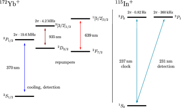
The possibility to detect the quantum information of the clock excitation directly via the state with a natural lifetime of 0.44 s ( kHz) Peik can facilitate the atomic signal read-out of a larger chain of ions, without the need of quantum logic technique Schmidt . Its transition wavelength of 230.5 nm can be generated with standard diode laser technology and second harmonic generation Schwedes . Due to the lower cooling power obtained by laser cooling on this narrow transition and the increased rf heating in Coulomb crystals, it is still advisable to sympathetically cool the indium ions with a second ion species with a stronger cooling transition. In our case we choose 172Yb+, because of its long lifetime in ion traps, the all-diode-laser based easy accessible wavelengths and the similar ion mass, that allows for efficient sympathetic cooling. YbH+ formed in collisions with background gas can be dissociated with the Doppler cooling light Sugiyama . In addition, the 172Yb+ isotope has no hyperfine structure and cooling is facilitated. Besides the enhanced cooling efficiency and control of ions, the presence of a second species allows for the possibility to sympathetically cool during the clock interrogation in case of excessive heating, additional characterization of the trap environment, such as magnetic fields, and an alternative clock read-out via quantum logic for comparative studies.
Besides the absence of electronic quadrupole moment, the 10 transition in 115In+ has the advantage of a very low sensitivity to environmental effects, which are summarized in table 1.
| Type of shift | Shift | Uncertainty |
| in | in | |
| Thermal motion (T=0.5mK) | 1 | 1 |
| Heating∗ | 0.1 | 0.1 |
| Excess micromotion | 1 | 1 |
| 2nd order Zeeman | 0.1 | 0.1 |
| BBR at 300K | 13.6 | 1 |
| DC Stark | 0.08 | 0.08 |
In particular, indium profits from its heavy mass when considering relativistic frequency shifts (second-order Doppler shift) due to time dilation , where is the kinetic energy of the ion, its rest mass, the speed of light and the frequency of the atomic transition. At the Doppler cooling limit mK of 172Yb+ this frequency shift amounts to , where is the kinetic energy due to thermal secular and micromotion in a linear ion trap Berkeland . If relative uncertainties below are targeted, further cooling such as sideband cooling of the Yb+ ion or direct cooling on the intercombination line of the 115In+ ion Peik_1999 can be implemented, where temperatures of K can be reached. An additional kinetic energy can be brought into the system by excess heating due to thermally activated patch potentials and contaminations on the electrodes Deslauriers ; Bergquist_Rosenband_Science . Assuming an enhanced electronic field noise with a power spectral density of (V/m)2Hz-1 in our ion trap with electrode-to-ion distance of 0.7 mm, see figure 6 in Epstein , we obtain a maximum relative frequency shift of due to heating of the secular motion during the clock interrogation, corresponding to 5 phonons at an eigenfrequency of the secular motion = 1 MHz. Here we assumed a maximum clock interrogation time of 100 ms, limited by the natural lifetime of the state of 115In+. Commonly observed heating rates in such ion traps can be a factor 10 to 100 lower Epstein , giving relative frequency shifts of and below.
Regarding ac Stark shifts due to blackbody radiation (BBR), 115In+ has one of the smallest sensitivities among optical clock candidates. With a differential static polarizability of Hz/(V/m)2 between the and state Safronova , it is comparable to 27Al+ Safronova ; Rosenband_BBR . Here, dynamic corrections due to the frequency distribution are neglected, as they are typically of the order of a few percent or below. At room temperature this corresponds to a blackbody shift of the clock transition of . For example, determining the temperature of the trap environment to ∘C will give a relative clock uncertainty due to the blackbody shift of .
Two major systematic frequency shifts arising from imperfections in the rf trapping potential are excess micromotion (EMM) and dc Stark shifts. If the driving radiofrequency field of the trap cannot be zeroed at the place of the ion, it amounts to a second-order Doppler shift of , where is the electronic charge, the amplitude of the electric rf field at the place of the ion and the trap drive frequency Berkeland . This effect is the dominating uncertainty in today’s best ion clocks and aggravates for a larger number of ions. Section 4 of this paper addresses the influence of finite size effects of the trap and imperfections in the electrode machining on the rf field in detail. The targeted upper limit in our trap design for residual rf fields on the trap axis is a maximum of 90 V/m, which corresponds to for a trapped 115In+ ion at a trap frequency MHz, as discussed in section 3.1. In addition, any residual electric field seen by the ion, will give rise to a dc Stark shift in the clock transition. Here, 115In+ profits from its low static differential polarizability Safronova . At an rf field amplitude of 90 V/m this Stark shift corresponds to .
Lastly, we consider the influence of static and dynamic magnetic fields in the ion trap. The linear Zeeman shift from the to states amounts to 6.36 kHz/mT Becker and is due to hyperfine mixing of and states (the nuclear spin of 115In is ). It can be measured and subtracted by alternatively pumping the ion into the stretched states of the ground state with opposite magnetic moments Madej ; Bergquist_Rosenband_Science . The second-order Zeeman shift is given by , where for the alkaline-earth like system Hz/mT2, where is the Bohr magneton and the Planck constant. Owing to the large fine-structure splitting Hz of the excited triplet states, indium has an advantageously low second-order B-field dependency, 10000 times lower than 171Yb+ and 20 times lower than 27Al+. Due to unbalanced currents in the ion trap alternating magnetic fields with T2 have been observed in ion traps Chou . For 27Al+ this accounts for an ac Zeeman shift of . For the 115In+ ion with this effect is negligible at the level of . While static and dynamic B-fields can be determined quite accurately and frequency shifts can be taken account of, for an optical clock based on many ions, requirements on the homogeneity of magnetic fields become important. With a linear Zeeman shift of 6.36 kHz/mT variations in magnetic field amplitude should be less than 16 nT across the ion chain to ensure that the broadening of the atomic line is less than 0.1 Hz. Distortions of the line profile due to spatially varying systematic shifts will have to be evaluated carefully to avoid locking offsets. The fast interrogation cycle, that is possible with a multi-ion frequency standard, will be advantageous when both stretched states are probed, in order to avoid offsets due to temporally varying magnetic fields.
The above considerations show that it should be possible to evaluate the clock frequency of a larger sample of 115In+ ions with a fractional frequency uncertainty of , assuming that a sufficiently ideal trap can be machined, which will be addressed in more detail in the following sections of this paper. We have not addressed other potential systematic frequency shifts like Doppler effects of first-order Bergquist_Rosenband_Science or phase-chirps in acousto-optic modulators, which are of general technical origin and need to be evaluated in each individual experimental setup. Frequency shifts due to collisions with the background gas have to be studied, but are typically in the range when operating the ion clock at a background pressure in the low Pa range Bergquist_Rosenband_Science .
3 Trap design
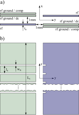
For an optical clock with low systematic frequency shifts and competitive long term stability it is important to have a high level control of the electrostatic and magnetic fields seen by the ions over the whole trapping region. This includes both necessary external control and 3D optical access to measure micromotion and field shifts. We consider a scalable segmented trap design, see fig. 2, in which ions can be trapped either in a long linear string with an axial anharmonic dc potential Lin or, in an harmonic axial confinement, in separate “buckets” of up to 10 ions in every other trap segment, that can then be controlled independently. Compared to linear ion trap designs with separate dc electrodes on the trap axis for the axial confinement Naegerl , segmented rf electrodes Schulz ; Madsen give a more ideal behavior of the rf field lines along the axial trap direction and allow for a high precision in the alignment of trap electrodes, if machined from one part. Currently a laser cutting and metallization process for low rf loss ceramic wafers is being developed in our lab. Four of these wafers can be precision aligned and stacked on top of each other to give the trap assembly.
Figure 1(b) shows the top view onto one pair of rf quadrupole electrodes, that can be laser cut from one thin wafer. To the segmented rf ground electrodes different dc potentials can be applied for the axial confinement as well as for static stray field compensation in the axial and one radial direction. To obtain both degrees of freedom to compensate for residual micromotion in the radial plane, our design includes an additional electrode wafer with compensation electrodes that overlie each rf ground/dc electrodes with a small spacing in the range of 0.1 mm to 0.25 mm, see fig. 1(a). The dc field generated by these extra compensation electrodes as well as their effect on the rf field is described in section 4.7. Our trap design is rather open and offers optical access in the plane and in the plane for laser beams necessary for laser cooling, exciting repumping transitions, state manipulation and probing. In direction, with a typical electrode thickness between 0.2 mm and 0.4 mm, a solid angle fraction larger than 4 % is available for optical fluorescence detection.
3.1 Trap parameters
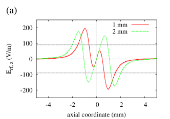
In order to reduce heating of the secular motion of the ions we have chosen a rather large distance mm from the electrodes to the trap center, since observed excess heating rates scale as Deslauriers ; Epstein . The geometry of the linear quadrupole electrode assembly has unity aspect ratio, with a distance of 1 mm between the tips of opposite electrodes, as shown in figure 2(a). For this case, the quadrupole term of the radial rf potential is only a factor 1.3 lower than in an ideal Paul trap with hyperbolically shaped rf electrodes. In this sense, the trap geometry is relatively efficient and sufficiently large trap frequencies of secular motion in radial direction can be realized despite the large distance to the trap electrodes. With an rf voltage amplitude of 1.5 kV at an rf drive frequency MHz we obtain trap frequencies for the secular motion of MHz and MHz for 172Yb+ and 115In+ ions, respectively.
An important criterion for first-order Doppler free clock spectroscopy is the Lamb-Dicke condition with Dicke . Here, is the rms spread of the position of the ion and is the modulus of the wave vector of the light exciting the transition. At an ion temperature corresponding to the Doppler limit for Yb+, 0.5 mK, the Lamb-Dicke parameter in radial direction takes a value of for the indium clock transition at 236.5 nm. For the ground state of the harmonical oscillator, with MHz, .
The confinement in axial direction is generated by applying a dc potential between neighboring segments in the rf ground electrodes. For an harmonic confinement inside the Lamb-Dicke regime, every other segment can be used as an ion trap with one segment for dc confinement in between. We find that the curvature of the axial trapping potentials has a shallow maximum as a function of segment length close to 1 mm dropping off by 10% at 0.8 mm and by 7% at 1.2 mm. Regarding the number of traps obtained per unit length of the quadrupole electrodes it seems desirable to use a smaller segment length. However, for segment lengths smaller than 1 mm neighboring traps become less well isolated from each other in the sense that varying compensation voltages in one trap are sensed by neighboring ion traps. In addition, the depth of the static potential well on the trap axis decreases monotonically with decreasing segment length . As will be described in section 4.3 the choice of the segment length also influences the axial component of the rf field, as far as the contribution from the notches and isolation slits in the quadrupole electrodes is concerned. For our design, we consider segment lengths in the range from 1 mm to 2 mm.
In an ideal linear Paul trap the rf field vanishes along the symmetry axis of the ion trap and driven micromotion of the ion can be minimized for a linear string of ions. To prevent transitions of the linear chain of ions to zig-zag, helical and more complex crystal structures, the ratio of radial to axial trap frequencies of secular motion has to be kept above a critical value, which depends on the number of ions in the crystal. The various phase transitions in the ion Coulomb crystal were investigated numerically and analytically Schiffer ; Dubin ; Totsuji . Estimates for the critical ratio for the transition from the linear crystal as a function of from different authors are in agreement with each other and are compiled in reference Wineland_Monroe . Using the criterion obtained by Steane Steane , we find, for example, for five ions and for ten ions. Choosing 1.75 MHz for the linear confinement of ten ions is possible for MHz.
3.2 Design criterion: micromotion in linear rf trap
A principal limitation in today’s optical ion clocks are frequency shifts induced by excess micromotion Berkeland . The observed EMM can originate from uncompensated static stray fields that shift the ion off the nodal line of the rf field, residual phase shifts of the rf potential on opposing electrodes and imperfections in the ion trap geometry that lead to a non-vanishing rf field along the trap axis. Our design allows to compensate static stray fields for all degrees of freedom in the radial plane to zero micromotion radially. RF phase shifts can be suppressed by carefully designed electronic circuits, symmetric leads and low resistivities. The electronic circuit scheme of our scalable trap design is currently tested on a first prototype trap tbp . In this paper we focus on the minimization of residual rf fields along the trap axis, that are due to the trap geometry and cannot be zeroed, thus severely limiting the available trapping region, where micromotion is negligible.
The dominating frequency shift due to EMM is the second-order Doppler shift, while dc Stark shifts induced by residual rf fields are roughly an order of magnitude smaller in the case of ions with low static polarizabilites, such as 115In+ and 27Al+, see section 2. We therefore assume as a trap design criterion a maximum second-order Doppler shift of due to residual axial rf fields.
As already pointed out in section 2, this relativistic frequency shift contributes with to the fractional uncertainty of the optical clock. Here, the kinetic energy of the ion of mass is given by the contributions from the secular motion and from the micromotion of the ion. Assuming the secular motion to be thermalized at a temperature one obtains for the three degrees of freedom of motion with denoting the Boltzmann constant. For the radial degrees of freedom in a linear Paul trap, assuming the confinement is given by a purely quadratic pseudopotential
| (1) |
the thermal contribution of micromotion to the kinetic energy is equal to the kinetic energy contribution from the secular motion , a result obtained from both classical and quantum-mechanical treatment of the ion motion Wineland_Itano_1987 . This is the case when the EMM is reduced to a negligibly small level in the radial directions and when the contribution of the static potential to the radial confinement can be neglected. The static potential has a weakening effect on the radial confinement and thus results in an increase of the micromotion contribution to the kinetic energy which can be calculated using equation 10 in reference Berkeland . In an ideal trap the axial confinement is purely given by the static potential. The micromotion contribution to the kinetic energy in axial direction can only stem from excess micromotion due to a residual axial component of the rf field along the trap axis. Neglecting the contribution of the static potential to the radial confinement we obtain
| (2) |
when the excess micromotion in radial directions is reduced to a negligibly small level, which is possible using techniques described by Berkeland et al. Berkeland and taking care in the design of the rf circuit to minimize rf phase shifts between the quadrupole electrodes to a negligibly small level.
As the second term on the righthand side of equation 2 suggests, the axial component of the rf field has to be considered separately. Although a single ion or a linear chain of ions may also be displaced in axial direction in the trap by applying a dc electric field in search for a minimum in , the existence of a minimum and whether the minimal magnitude of is small enough is determined almost entirely by the design of the trap and the strict keeping of tolerances in its construction. Hence, in the design of the trap we look for geometries which minimize the axial component of the rf field and analyze the sensitivity of different sizes in the geometry in order to state the tolerances for the construction.
For indium ions using an rf drive frequency MHz and an rf amplitude of 1.5 kV a residual axial rf field amplitude of 90 V/m amounts to a relative frequency shift of due to non-thermal EMM, second term in eq. 2. In order to minimize the axial micromotion for a linear chain of 5 to 10 ions to that level, in each trapping segment a region of a length of 50 m to 100 m is required along the axis, where the magnitude of the axial rf field is no larger than V/m.
4 Trap field calculations
An ideal infinitely long linear Paul trap has no axial rf field component. In segmented linear Paul traps of finite length used in practice, a nonzero axial rf field component on the trap axis appears for several practical or technical reasons, which we investigated in order to minimize their effect. These are: the finite length of the quadrupole electrodes; insulation gaps in the dc electrodes; deviation from the ideally parallel alignment of the quadrupole electrodes to the trap axis; differences in the geometry of the electrodes and insulation gaps that breach the symmetry.
For the trap field calculations in sections 4.2 through 4.6 an electrode geometry similar to figure 2 is used, with a varying number of segments, as will be indicated in the text. Only the layers of extra compensation electrodes are omitted, in order to preserve symmetries and to separate the different effects. The effect of these extra layers on the rf field is discussed in section 4.7.
In order to obtain the ponderomotive potential given in equation 1, the electric field of the linear Paul trap is calculated. The Laplace equation is solved for boundary conditions given by the electrodes. As this is a linear homogeneous differential equation, a solution for a specific boundary condition can be written as a linear combination of solutions of this geometry. It is worthwhile noting that a better understanding of the effects can be gained by decomposing the electrostatic potential problem linearly into one component containing only the almost ideal part of the potential producing the quadrupole trap potential and a second component, which contains mainly the effect of the trap imperfection under investigation. In our experiment we use a configuration with two diagonally opposite electrodes put on rf voltage keeping the other pair at rf ground. The potential in this configuration is denoted by . It can be thought of as sum of the configurations and . The configuration generates the quadrupole potential required for trapping and by symmetry has zero voltage everywhere on the trap axis. Therefore, for the ideal symmetric trap, this configuration has no axial rf field component. The configuration generates a flat nonzero potential between the quadrupole electrodes with almost zero electric field in the neighborhood of the trap axis. It displays finite size effects and effects of the segmentation slits onto the on-axis electric field clearly.
It can also be advantageous to apply this decomposition method when calculating the trap potential using the FEM. The precision achieved at a given mesh point density increases with decreasing electric field. Thus, effects which appear mainly in the configuration, which does not contain the strong radial trapping field gradients, can be calculated with higher accuracy. The dependence of the accuracy of the solution on the electric field is accounted for by the definition of the residual error estimation function Goering_fem , which plays an important role in approximating iterative linear solver methods employed in the solution of FEM problems as well as in adaptive mesh refinement routines.
We estimate the accuracy of our calculations to resolve the axial component of the rf field on the trap axis on a level well below 90 V/m at an rf amplitude of 1500 V. Regarding the large radial field gradients of V/m2 obtained at this rf amplitude, this is demanding as the mesh elements in the region of the trap axis typically have a size in the range of 0.05 mm to 0.1 mm and hence, fields on their surfaces are on average orders of magnitude larger.
To reach the required accuracy we followed the mesh generation strategy with adaptive mesh refinement steps described in Section 4.1 until a convergence at the low percent level is reached. Where applicable, symmetry planes are used in the FEM model to reduce the size of the problem and hence required computing power. For the trap model of section 4.2 and 4.3, the linear decomposition into the configurations and could be exploited and thus, higher accuracy reached at the same use of computing resources. For these calculations we obtained accuracies better than 10 V/m for the axial component of the rf field on the trap axis.
4.1 Technical details of the finite element calculations
For the calculation of the rf trap potential, it is sufficient to consider the rf field at a fixed phase, such that the field calculation reduces to an electrostatic problem. Dynamic effects due to the electronic lead design that can produce different phase shifts for the rf field at different points in the trap have been considered with a separate rf electronics software and will be discussed for the prototype trap tbp .
The calculations of the rf field presented in this work consist in finding the solution to the electrostatic Dirichlet problem, in which the electrode surfaces of the trap are the boundaries kept at given electric potentials. We use a commercially available software (COMSOL Multiphysics 3.5) for finite element analysis. In our FEM model we surround the trap electrode assembly with a wide rectangular boundary box, which is set to ground potential. The sides of the grounded box are typically at a distance of 1-2 cm from the trap electrode surfaces. We verified for different box sizes from 7 to 30 mm that this distance was large enough to have no influence on the obtained results.
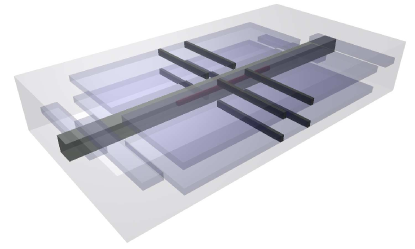
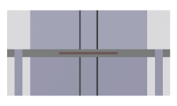
Dielectric components required in the actual implementation of the trap were not taken into account in our field calculations, since they are either far away from the trap region or their surface is almost entirely coated with conducting electrode material. The electrode surfaces are represented in the geometry model of the trap simulation by an assembly of rectangular boxes of 5 mm depth and of variable width and thickness as then stated in the text. An example of a geometric model used in a calculation for a trap made of three segments is schematically drawn in figure 3.
To generate the mesh we used the routines provided by the FEM software. The mesh elements are of tetrahedral shape. Quadratic Lagrange element functions were used in our calculations, with the exception of the calculations presented in Fig. 11 as here the use of quartic Lagrange element functions led to a slight improvement in the quality of the solution. As control parameters for the mesh generation we mainly used the maximum mesh point separation and its growth rate in transitions from regions where a higher mesh point density is required to regions where it can be lower. In order to have an independent control over the mesh generation in different regions of the geometry, we define various domains where dedicated mesh generation parameters can be applied (see Fig. 3).
An initial mesh is generated with the maximum mesh point separation set equal to a fraction of the smallest distance in the surrounding local geometry and the element growth rate to values between 1.1 and 2. We changed mesh control parameters in the special mesh domains we had defined and compared the results of the calculation. We found that choosing small element growth rates in the range from 1.1 to 1.5, i.e. keeping mesh point density gradients small, was important to obtain convergence of the result with increasing mesh point density. Starting with a mesh, improved by the convergence analysis with manually changing mesh parameters, we additionally apply the adaptive mesh refinement routine of COMSOL. During the solution of the problem this routine detects the regions where improvements to the mesh are most effective in increasing the accuracy of the calculation. It accordingly improves the mesh quality and recalculates the solution. Typically after two or three adaptive mesh refinement steps we found that, regarding the axial component of the field on the trap axis, the relative change between two consecutive adaptive mesh refinement steps had decreased to a level on the order of .
The number of degrees of freedom or unknowns of the linear system of equations for our problem was typically in the range between and . Only approximating iterative solver methods are practicable for problems of this size and the computer memory at our disposal. In our case mostly an iterative conjugate gradient method with algebraic multigrid preconditioning and an iterative geometric multigrid method were used in combination with the direct solvers PARDISO and UMFPACK. As computer hardware we used two desktop computers, of which one has 4 gigabytes and the other has 16 gigabytes of main memory.
4.2 Effect of the finite length of quadrupole electrodes
For an electronically symmetric trap configuration
the electrostatic
potential along the trap axis is 0. Therefore, the electric field
lines show no axial field component along the entire trap axis.
For an highly segmented rf trap, where trapping electrodes are
used simultaneously for dc compensation, it is technically very
challenging to deliver multiple independent rf voltages to the
various electrode segments with identical amplitude and phase.
Therefore, for the scalable trap design we chose the
configuration, where one rf trap electrode
is kept on rf ground, facilitating independent adding of dc
voltages. In this configuration the electrostatic potential on the
trap axis is roughly and electric field
gradients along the axis are observed when terminating the rf trap
electrodes to a finite size. In order to keep this axial component
of the rf field amplitude below a given value, we adjust the
minimum length of the trapping electrodes. For our linear Paul
trap with a 1 mm 1 mm electrode spacing,
figure 4(a) shows the axial component of
the rf field along the trap axis plotted over the axial coordinate
for various lengths of the quadrupole electrodes. Here, the
electrode thickness mm and, for simplicity, an electrode
geometry without notches was used.
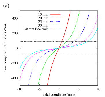
Our trap design also includes grounded electrodes at the ends of the quadrupole electrodes perpendicular to the trap axis behind a 1 mm insulating slit, as shown in figure 3. The purpose of the grounded end electrodes is to provide a defined electrostatic potential between the ends of the quadrupole electrodes of the trap, where otherwise the insulator material of the wafer would be exposed. For the calculations shown in figure 4(a) the grounded end electrodes are included in the trap geometry. For comparison, for an electrode length of 30 mm both cases are shown, with grounded and without grounded electrodes (free ends curve).
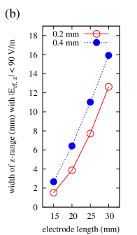
Requiring an axial rf field component of magnitude smaller than Vm, we can find the width of the range on the trap axis usable for trapping of clock ions. In figure 4(b) the width of this usable range is plotted as a function of the length of the quadrupole electrodes. When we segment the quadrupole electrodes using a segment length of 1 mm, for example, with a total length of the quadrupole electrodes of mm and an electrode thickness of mm, our design can accommodate a linear array of six usable ion traps for the clock application. The number of usable traps decreases rapidly when the total electrode length is shortened. With cm and mm the number of usable ion traps is already reduced to two. For an electrode thickness of 0.4 mm the corresponding usable range for clock application is given in figure 4(b) as well. In comparison to mm, we obtain a moderately increased number of suitable traps: eight with an electrode length of 30 mm and three with a 20 mm electrode length.
With a view to further miniaturization of trap assemblies and further increase of the number of trap sites, it would be desirable to find a way to avoid long trapping electrodes. By introducing an additional rf ground electrode above and below the rf electrodes the effect of finite length of the trap electrodes can be decreased substantially, such that more trap segments can be used with the same or an even smaller length of trap electrodes. Enclosing the linear quadrupole electrodes by extra ground electrode layers from above and below forces equipotential surfaces of the rf potential to flatten out over a wide range of the trapping area, as shown in figure 5 (right). With electric field lines being orthogonal on equipotential surfaces, this results in a smaller gradient of over much of the axis, with a steeper increase only close to the ends of the trap array.
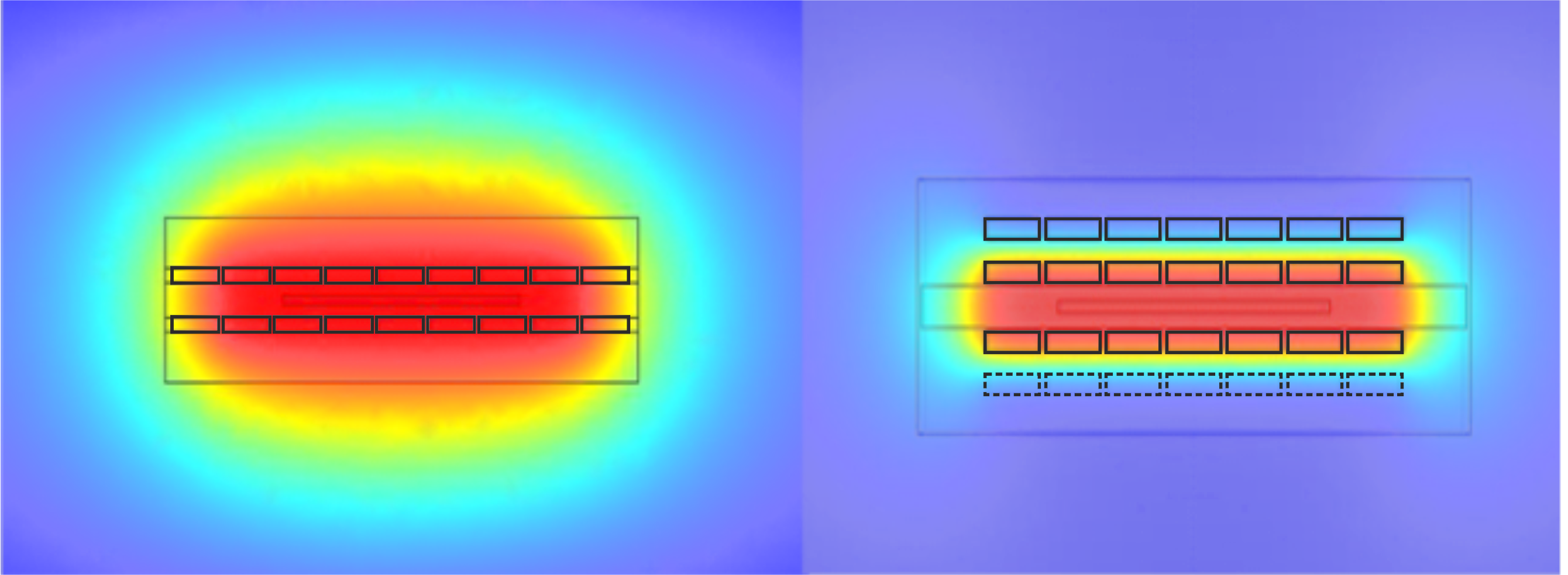
However, there are several drawbacks of the additional rf ground electrode layers, which are more or less important depending on the choice of electrode thickness and electrode layer spacing: the capacitance of the trap is increased; the numerical aperture for optical detection can become limited by the electrode assembly; increased risk of electrical breakdown; and finally, the axial rf field component on the trap axis resulting from notches in the electrodes is considerably intensified. As operating a 30 mm long ion trap in our setup brings no further limitation for the moment, we did not include this option in our current trap design. Additional electrode layers are chosen only for extra compensation on top of the rf ground electrodes as shown in figure 2, that can then be put substantially closer.
It is worthwhile mentioning that plotted in figure 4(a) can be well approximated in the central region on the axis using the expression
| (3) |
which gives the axial component of the field of a line charge of length in the distance from the axis and with unit line charge density. For values closer to the ends of the quadrupole electrodes the calculated field component deviates strongly from this expression as here the approximation using a constant line charge density can obviously not be made. Using a least square fit of this expression to the FEM calculation results for the axial electric field we obtain values for , and a proportionality factor for different lengths of the quadrupole electrodes. In the calculations presented in the following paragraphs it was helpful to use a smaller length of the trap electrodes in order to keep the size of the problem smaller. To better isolate the effects under investigation we subtracted the finite length effect in form of the mentioned fit function from the FEM results.
4.3 Effect of insulation slits in dc electrodes
In our design the rf ground electrodes also serve to apply dc voltages for axial confinement of the ions and to generate electric compensation fields in axial and in one radial direction. The electronic insulation of the electrodes requires segmentation slits. Here a notch is machined into the underlying insulator material and a conductive layer is applied around the teeth structure to cover insulation material in direct view of the ions, still leaving each tooth electrically insulated from its neighbors.
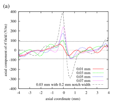
Electrode surfaces of the trap assembly are equipotential surfaces of the electrostatic problem. The introduction of insulation slits into the electrode geometry causes a receding of equipotential surfaces in their vicinity. This receding is of course more prominent closer to the electrode. Further away, it is increasingly smoothed out and the curvature it causes in the equipotential surfaces is reduced. Still, in the neighborhood of the trap axis a net effect of insulation slits in the electrodes is noticeable. Implementing corresponding symmetric notches in the rf electrodes can partially compensate for this effect. This can be understood when decomposing the corresponding electrostatic problem linearly into the two configurations and . For the contribution of the configuration it is clear that keeping an exact geometric symmetry between the rf and rf ground electrodes leads to a zero potential all along the trap axis. On the trap axis, the effect of notches in the rf ground electrodes is then exactly cancelled out by the effect of the corresponding notches in the rf electrodes. However, even if the symmetry of the geometry is intact, there will be a residual magnitude in the axial component of the rf field which stems from the contribution of the configuration and can not be compensated by symmetry. The potential on the trap axis in this configuration is a certain amount smaller than , depending on how open the electrode structure is. For trap electrodes, for example, being further apart from each other, the electrostatic potential on the trap axis is smaller. This seems to be exactly the effect of the notches in the electrodes, the equipotential surfaces are receded closer to the notches, leading to a minimum in the rf potential on the trap axis and resulting in a dispersion-shaped behavior of the axial component of the rf field. Figure 6 shows the calculation of this effect for different widths of the notches in the electrodes.
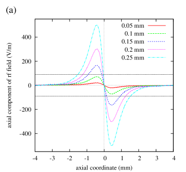
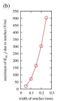
In this calculation a thickness of 0.2 mm was assumed for the electrode blades. To highlight the effect of a single segmentation, a trap geometry with only one notch per electrode blade was simulated. All four notches of the quadrupole electrodes are located at .
We also calculated the effect for different electrode thickness. The maximum magnitude of the axial component of the rf field obtained for different electrode thickness is given in figure 7 for a fixed notch size mm.
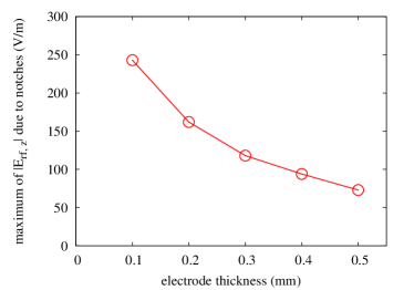
Using thicker electrodes is obviously advantageous regarding the contribution of the notches to the axial component of the rf field. This can be an interesting option when the electrodes are made using a technique different from the one we chose. Both laser cutting of thin wafers and the subsequent metallization are more difficult for thicker structures and higher aspect ratios.
For a segment length of a few mm and smaller, the effects of the notches from both ends of a segment cancel partially. The behavior of the resulting axial rf field in the middle of the segment varies with the segment length, since it is composed of contributions from both ends of the segment, which have opposite sign. Figure 8(a) shows the simulation of a trap with three segments, thus two discontinuities in the electrode blades. The inner segment length is mm and mm, respectively, with the width of the notches kept at 0.15 mm and electrode thickness at 0.2 mm. Here, the center of the inner segment is at .
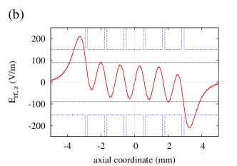
The curve for the 1 mm long segment shows, that the effects of the notches from both sides of the segment are partially cancelling each other. This can also be seen in the calculation for a trap with five inner segments of 1 mm length shown in figure 8(b). We can conclude, that if the symmetry of the electrode construction is given, the remaining axial rf field component produced by the notches in the electrodes is small enough to allow trapping of ion chains of five to ten ions for clock applications. Even if a larger width of the notches is chosen, close to the center of each trap segment the axial rf field component has a zero crossing resulting in a range with V/m large enough to accommodate a chain of ions.
4.4 Angular misalignment of quadrupole electrodes
Due to the precision achieved in the process of laser machining of 1 or 2 m, we can assume that electrodes located on one wafer can be aligned nearly perfectly with respect to each other. Thus, we only need to consider angular misalignment of the two quadrupole electrode pairs occurring during the trap assembly.
First, we consider a possible rotation angle between the two wafers of the quadrupole trap electrodes around the axis normal to the wafer plane, corresponding to the axis in figure 2. Figure 9(a) shows the axial component of the rf field calculated for an electrode thickness of 0.2 mm for different misalignment angles using a configuration. Here, the trap axis is rotated by the angle .
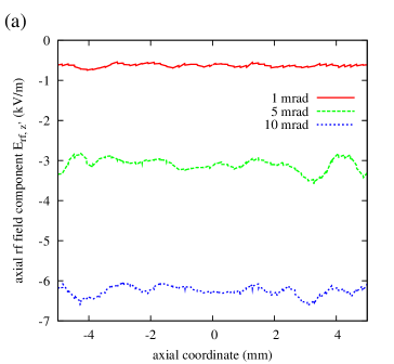
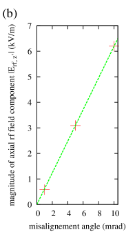
Our calculations show that this angular misalignment produces an rf field component along the trap axis, which is proportional to the angle of rotation of the two electrode layers with respect to each other. This can be seen from figure 9(b) which shows a plot of as a function of the rotation angle. When repeating the calculation for an electrode blade thickness of 0.4 mm the results for the axial rf field component show no significant difference compared to the results obtained with 0.2 mm electrode thickness. We deduce from figure 9(b) an axial rf field of V/m per mrad. In order to keep this axial rf field component well below 90 V/m we have to ensure that the angular misalignment of the two wafers for rotation around the -axis is less than 0.14 mrad.
Second, we consider an angular misalignment of the two electrode wafers with respect to each other around the axis of rotation corresponding to the axis (see fig. 2). An angular misalignment around this axis can occur during the assembly of the electrode wafers, when, for example, the spacer height is not identical, or glue is creeping between spacer and electrode blade. Such a misalignment leads in first order to a linearly changing distance between the electrode wafers along the trap axis. This obviously leads to a corresponding change in the radial rf field gradients and consequently of the radial trap frequencies for the secular motion and a small variation of the on-axis potential is to be expected as well. In our calculations we used misalignment angles in a range from 1 mrad to 10 mrad. However, within the estimated accuracy of the calculation, which is well below 90 V/m on the trap axis, we could not resolve any deviation from zero in the axial rf field component due to angular misalignment of this type.
4.5 Tolerances on width and position of notches in electrodes
In the process of machining notches into the electrode blades inaccuracies can occur in both the positioning of the notches as well as in their width. The subsequent process of coating the insulator with the electrode material can also contribute to further inaccuracies.
First, we consider the effect of a small change in the width of one of the four notches separating two segments of the linear Paul trap. We calculated the resulting rf field when one notch is made wider in one rf carrying electrode. Our calculations show what can be expected from such a change in the geometry: an additional receding of the equipotential surfaces away from the widened notch occurs, centered at the axial coordinate of the notch. As a result the axial rf field component displays a dispersion-shaped behavior along the -axis at the edge of the trap segment in excess of the magnitude found for a symmetric electrode geometry as shown in figure 6(a). The radial components of the rf field as well display on the -axis an increase from zero which peaks at the location of the widened notch. The feature in the radial field components is of similar width and amplitude as the one in the axial component. Due to the strong gradient in the radial rf field components the excess field produced by the widened notch leads to a small bending of the actual trap axis away from the -axis by a distance on the order of nm.
Figure 10(a) shows the axial rf field component as a function of the axial coordinate obtained for different positive deviations in the width of one notch from the width of the notches in the other three electrodes, which are kept at mm.
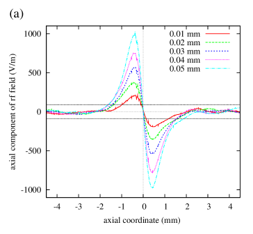
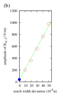
The dependence of the amplitude of the dispersion-shaped feature in the axial rf field component on the deviation in the width of one notch is shown in figure 10(b). The line in the graph resulting from a least square fit suggests, that the dependence can be regarded to be linear in this range. Assuming a segment length of mm, we deduce a maximum tolerance for the notch width in the rf carrying electrode of m in order to have V/m in the middle of the segment. For a segment length of 2 mm the middle of the trap segment is further away from the segment border and the region where peaks, such that notches can be cut to less stringent tolerances of m.
By widening a notch in an rf ground electrode instead of in an rf carrying electrode we find in our calculations a very similar effect in the axial component of the rf field on the trap axis, albeit smaller in amplitude, by roughly 20% for the here considered geometry, and of opposite sign.
We also varied the design width of the electrode notches in the range from 0.1 mm to 0.2 mm and observed a linear increase of the amplitude of the effect of a widened notch with increasing . The amplitude of the effect was increased 1.8 times for a design notch width of 0.2 mm as compared to a design notch width of 0.1 mm.
The calculations in figure 10 have been carried out for an electrode thickness of mm. When we repeated the calculations for mm we found only a small increase in the magnitude of by a factor of 1.07 for a design notch width of mm and by a factor of 1.15 for mm.
Second, we consider an inaccuracy in the position of one notch in an otherwise perfectly symmetric electrode assembly. Figure 11 shows the effect on when one notch is displaced in positive direction.
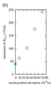
On the axial component of the rf field the effect is asymmetric with a maximum located around the center of the notches followed by a minimum of smaller magnitude located around mm. The magnitude of the additional axial rf field produced by a position inaccuracy is considerably smaller than that found for inaccuracies in the width of a notch. Since the maximum of is also localized on the border of the segment the trap region in the center of the segment is even less affected.
For the calculations shown in figure 11(a) the notch width mm has been used with exception of one curve, for which the chosen notch width of 0.2 mm is pointed out in the legend of the graph. We observed a rapid increase of the maximum of as a function of the notch width, the displacement of one notch with respect to the others being kept constant. We want to point out that the residual axial rf field amplitude occurring in the perfectly symmetric case also grows rapidly with increasing width of the notches (see fig. 6) and can contribute significantly here. The curves in figure 11(a) have been calculated using an electrode thickness of 0.4 mm. When we used an electrode thickness of 0.2 mm instead, we did not find a significant increase in the effect.
Targeting a positioning accuracy of better than 10 m when aligning the different electrode layers on top of each other, the axial rf field contribution due to position inaccuracies will not become critical for a notch width of up to 0.2 mm.
4.6 Translational misalignment of quadrupole electrodes
We looked into the misalignment of the trap assembly in which one of the electrode wafers is translated with respect to the other parallel to the trap axis. The translation destroys the symmetry of the geometry at the end of the trap segments, where the notches in the electrodes of one wafer become displaced with respect to the corresponding notches in the other wafer. Considering such a pair of notches of which each is in another wafer, we expect that the displacement results in an extra axial component of the rf field halfway between the two notches. In our FEM calculations the extra axial rf field contribution was evident between the wafers in the vicinity of the notches.
The calculations also show that the extra axial field decreases in magnitude towards the trap axis to finally vanish right on the axis. Since for the pair of notches situated on the opposite side of the trap axis the configuration of rf and rf ground electrodes is reversed on the two wafers, the additional axial rf field component has opposite sign on both sides of the trap axis. As a result the effects of the translation from two opposite pairs of notches cancel each other on the trap axis. From our calculation using mm and mm we conclude that even at a distance of 0.05 mm from the trap axis and at coordinates corresponding to the location of electrode notches, an axial translation of 0.05 mm of the wafers with respect to each other results in a contribution to the axial component of the rf field smaller than 90 V/m. In the middle of the segment where the ions are trapped the effect is even smaller.
4.7 Introduction of extra electrode layers for dc field compensation
In order to compensate for dc stray fields in radial direction, which would displace trapped ions from the null field line of the rf field, the trap design has to offer a way to apply independent dc compensation fields in the radial plane in each trap segment. Two degrees of freedom are required to compensate for any electric field in the radial plane. Using a small voltage difference between the rf ground electrodes of the trap segment generates a dc electric field oriented in the (x,y) plane nearly along the (1,1) direction. In order to generate a second dc electric field with a strong component perpendicular to this axis, we considered two alternative designs.
In a first design, schematically drawn in figure 12(a), we added segmented compensation electrodes behind a 1 mm wide rf electrode with an insulation gap of 0.2 mm between rf and compensation electrodes. This design is compact but bears some strong shielding of the compensation electrodes by the trap electrodes. The FEM calculation of the dc field generated in this geometry with an electrode thickness of 0.4 mm, a segment length of 1 mm and a notch width of 0.1 mm gives a field of 8 V/m in the trap region of the segment using +1 V and -1 V on the extra compensation electrodes of the segment. Also in the next and second to next neighboring segments considerably large dc fields of 4 V/m and 1.4 V/m are found.
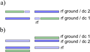
A second design consists in expanding the two-layer quadrupole trap assembly by two additional layers with dedicated segmented compensation electrodes. Fig. 12(b) gives a schematic view of this design. The additional layers are similar to the other two trap layers only that the rf electrode side is missing. Each extra layer is placed with a spacing of 0.25 mm on top and precisely aligned with a segmented rf ground electrode. The geometry of the extra compensation layers is kept identical to the inner trap electrodes regarding notch width and electrode thickness. The FEM calculation of the dc field generated by this geometry using an electrode thickness of 0.4 mm, a segment length of 1 mm, and a notch width of 0.1 mm gives a stronger field value in the trap region of 60 V/m for the voltages of +1 V and -1 V on the two extra compensation electrodes. The direction of the generated field vector points mainly along the -axis with a component of 3.7 V/m along the -axis. The corresponding field values obtained in the next and second to next neighboring segments are 19 V/m and 2.5 V/m, respectively.
The second design has a clear advantage over the first design regarding the larger field. The field is also well localized on the trap segment with only a 4% contribution to the dc field in the neighboring traps. In addition, considering the relatively large rf voltage amplitude we envisage to apply, the second design is also less prone to rf breakdown and surface flashover than the first. The slightly larger layer stack reduces the solid angle for optical detection to an acceptable level.
Since we opt for the second design we investigate the effect of the extra compensation electrode layers on the rf field. It is important to examine how the additional compensation electrodes affect the axial component of the rf field produced by the electrode notches. Considering the effect on a single segment border we calculate the rf field for an electrode geometry with only two long segments, thus one central discontinuity in the electrode blades. Adding the extra compensation electrode layers to the trap geometry clearly increases the amplitude of the axial rf field component caused by the notches. Compared to calculations for the same geometry without extra compensation electrodes as described in section 4.3 (figure 6), we find that the amplitude of is increased by a factor of 3.6 for an electrode thickness of 0.2 mm and a notch width of 0.2 mm, and by a factor of 4.6 for an electrode thickness of 0.4 mm and notch widths of 0.1 mm as well as 0.15 mm. Although the extra compensation layers lead to a considerable increase in the axial rf field component on the segment borders, the axial rf field component can still be small enough in the region in the middle of a trap segment, because here again the effects stemming from neighboring segment borders partially cancel one another out. An example for this is given in figure 13 for three different design parameters: electrode thickness, notch width and segment length. Here, a three segment trap was simulated with the middle segment of length surrounded by two long outer segments.
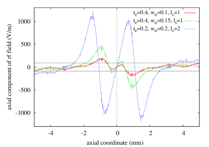
In the calculations for all three parameter sets shown in figure 13 an axial region of at least 0.12 mm length with V/m can be found, which is suitable for clock spectroscopy.
5 Conclusion and outlook
We presented an electrode design of a segmented linear Paul trap optimized for optical clock application and frequency standards based on the spectroscopy of Coulomb crystals. Using segmented electrodes the design supports the implementation of linear arrays of traps, where in each trap segment electrodes are provided for the compensation of dc electric fields in all three directions of space. The trap assembly still offers a good optical access for laser beams and fluorescence detection.
In this design geometry we propose to trap arrays of 115In+ ions sympathetically cooled by 172Yb+. We showed that with such an optical frequency standard of improved short-term stability a fractional long-term stability of can be reached with systematic frequency shifts at the mHz level. Integration times for the frequency measurement can be shortened by more than an order of magnitude and requirements for clock laser stability relaxed significantly.
Of great importance for high precision spectroscopy of a larger sample of ions is the minimization of excess micromotion of the ions, which can contribute considerably to the second-order Doppler shift of the clock transition. In our design we minimized the critical axial component of the rf field along the trap axis and studied tolerances for the manufacturing process of the trap. We identified and quantified the three most critical causes for excessive magnitudes of the axial rf field component: the finite length of the quadrupole electrodes; the tolerance on the width of the notches separating electrode segments; and the tolerance on the alignment angle of opposing electrode wafers (torsion around the axis in our coordinate system). For our choice of geometry with an 1 mm 1 mm spacing between the quadrupole electrodes, and requiring the axial component of the rf field on the trap axis to not limit the targeted fractional uncertainty of the frequency standard of , we can summarize our results on these critical effects as follows. Using a trap segment length of 1 mm and electrode thickness of 0.2 mm a linear array of six usable traps with at least 10 ions each is obtained with a total electrode length of 3 cm, whereas with a total electrode length of 2 cm our design only supports two usable traps. Choosing the width of the notches that are separating trap segments to be 0.1 mm and the segment length to be 1 mm, the tolerance on the width of a notch in the electrodes is m. The tolerance on the angular misalignment of the two quadrupole electrode layers around the direction orthogonal to the wafers is less than 0.14 mrad.
The effect of other tolerances in the trap construction, like the position deviation of a single notch in the electrodes, the translational displacement along the trap axis of one electrode layer with respect to the other, and the angular misalignment of the electrode layers around the axis, have also been investigated and quantified. We showed that their effect on the axial component of the rf field on the trap axis is either negligibly small or can be easily avoided by applying state-of-the-art tolerances in the manufacturing process. Further, we point out that depending on the choice of segment length boundary effects of the segmentations can cancel each other out, reducing the on-axis micromotion.
Based on our FEM calculations a prototype trap with two trapping segments made of Rogers4350BTM has been constructed and is currently under test. First measurements of micromotion with 172Yb+ ions show a promising low value in agreement with our simulations. For a scalable high precision trap we are developing a laser cutting and metallization process for AlN wafers, in which we plan to investigate an array of ions for an optical frequency standard.
Acknowledgments: We thank Ch. Roos for contributing ideas on trap field calculations and E. Peik for fruitful discussions and careful reading of the manuscript. This work was supported by the cluster of excellence QUEST.
References
- (1) W. Neuhauser et al., Phys. Rev. A 22, (1980) 1137.
- (2) F.G. Major, V.N. Gheorghe and G. Werth, Charged Particle Traps (Springer, Berlin 2010).
- (3) L. S. Brown and G. Gabrielse, Rev. Mod. Phys. 58, 233–311 (1986).
- (4) T. Rosenband et al., Science 319, (2008) 1808.
- (5) C. W. Chou et al., Phys. Rev. Lett. 104, (2010) 070802.
- (6) W. Itano et al., Phys. Rev. A 47, (1993) 3554.
- (7) D. Meiser et al, Phys. Rev. Lett. 102, (2009) 163601.
- (8) J. Millo et al., Phys. Rev. A 79, (2009) 053829.
- (9) T. Legero et al., JOSA B 27, (2010) 914.
- (10) A. Bjerhammar, Bull. Geodesique 59, (1985) 207.
- (11) N. K. Pavlis and M. A. Weiss, Frequency Control Symposium, 2007 IEEE International (2007) 642.
- (12) F. Riehle, Frequency Standards: Basics and Applications (Wiley-VCH, Weinheim 2005).
- (13) J. D. Prestage et al., Frequency Control Symposium, 2007 IEEE International (2007) 1112.
- (14) C. Champenois et al., Phys. Rev. A 81, (2010) 043410.
- (15) P. Schmidt et al., Science 309, (2005) 749.
- (16) T. Rosenband et al., Phys. Rev. Lett. 98, (2007) 220801.
- (17) D. Wineland and R. Blatt, Nature 453, (2008) 1008.
- (18) Th. Monz et al., arXiv:1009.6126v1 (2010).
- (19) Ch. Monroe et al., Phys. Rev. Lett 75, (1995), 4011.
- (20) Amini et al., arXiv:0812.3907v1 (2008).
- (21) D. Kielpinski et al., Nature 417, (2002) 709.
- (22) Q. A. Turchette et al., Phys. Rev. A 61, (2000) 063418.
- (23) D. Berkeland et al., J. Appl. Phys. 83, (1998) 5025.
- (24) R. H. Dicke, Phys. Rev. 89, (1953) 472.
- (25) K. Pyka et al., in preparation for New J. Phys.
- (26) Ch. Zipkes et al., Nature 464, (2010) 388.
- (27) E. Peik et al., Phys. Rev. A 49, (1994) 402.
- (28) T. Liu, Y. Wang, V. Elman, A. Stejskal, Y. Zhao, J. Zhang, Z. Lu, L. Wang, R. Dumke, T. Becker and H. Walther, Frequency Control Symposium, 2007 IEEE International (2007) 407.
- (29) J. A. Sherman, W. Trimble, S. Metz, W. Nagourney and N. Fortson, arXiv:physics/0504013v2 (2005).
- (30) Ch. Schwedes et al., Appl. Phys. B 76, (2003) 143.
- (31) Sugiyama et al., Phys. Rev. A 55, (1997) R10.
- (32) M.S. Safronova and M.G. Kozlov, arXiv:1105.3233 (2011).
- (33) T. Rosenband et al., Proceedings of the 20th European Time and Frequency Forum (2006) 289.
- (34) E. Peik et al., Phys. Rev. A 60, (1999) 439.
- (35) L. Deslauriers et al., Phys. Rev. Lett. 97, 103007 (2006).
- (36) R. J. Epstein et al., Phys. Rev. A 76, (2007) 033411.
- (37) J. E. Bernard et al., Opt. Comm. 150, (1998) 170.
- (38) Th. Becker et al., Phys. Rev. A 63, (2001) 051802.
- (39) Lin et al., Europ. Phys. Lett. 86, (2009) 60004.
- (40) H. C. Nägerl et al., The Physics of Quantum Information (Springer, Berlin 2000).
- (41) S. Schulz et al., New J. Phys. 10, (2008) 045007.
- (42) M. J. Madsen et al., Appl. Phys. B 78, (2004) 639.
- (43) D. J. Wineland et al., J. Res. Nat. Bur. Stand. Tech. 103, (1998) 259.
- (44) A. Steane, Appl. Phys. B 64, (1997) 623.
- (45) D. H. E. Dubin, Phys. Rev. Lett. 71, (1993) 2753.
- (46) H. Totsuji and J.-L. Barrat, Phys. Rev. Lett. 60, (1988) 2484.
- (47) J. P. Schiffer, Phys. Rev. Lett. 70, (1993) 818.
- (48) D. J. Wineland et al., Phys. Rev. A 36, (1987) 2220.
- (49) I. Babuska and T. Strouboulis, The finite element method and its reliability, (Oxford University Press, New York 2001).