Microscopic model for the ferroelectric field effect in oxide heterostructures
Abstract
A microscopic model Hamiltonian for the ferroelectric field effect is introduced for the study of oxide heterostructures with ferroelectric components. The long-range Coulomb interaction is incorporated as an electrostatic potential, solved self-consistently together with the charge distribution. A generic double-exchange system is used as the conducting channel, epitaxially attached to the ferroelectric gate. The observed ferroelectric screening effect, namely the charge accumulation/depletion near the interface, is shown to drive interfacial phase transitions that give rise to robust magnetoelectric responses and bipolar resistive switching, in qualitative agreement with previous density functional theory calculations. The model can be easily adapted to other materials by modifying the Hamiltonian of the conducting channel, and it is useful in simulating ferroelectric field effect devices particularly those involving strongly correlated electronic components where ab-initio techniques are difficult to apply.
pacs:
85.30.Tv; 85.75.Hh; 75.47.LxI Introduction
The research area known as oxide heterostructures continues attracting considerable attention of the condensed matter community due to the rich physical properties of its constituents, often involving strongly correlated electronic materials, and also for their broad potential in device applications.Dagotto (2007); Takagi and Hwang (2010); Mannhart and Schlom (2010); Hammerl and Spaldin (2011) Among these heterostructures, those involving ferroelectric (FE) and magnetic, or multiferroic, components are particularly interesting since they could be used in the next generation of transistors and nonvolatile memories.Ramesh and Spaldin (2007); Bibes et al. (2011); Nan et al. (2008) From the applications perspective, the FE/magnetic heterostructures could become even superior to the currently available bulk multiferroics with regards to their magnetoelectric performance.Ramesh and Spaldin (2007); Bibes et al. (2011); Nan et al. (2008) In these heterostructures, it is easier to obtain large FE polarizations and a robust magnetization, and the manifestations of the magnetoelectric coupling can be fairly diverse. For example, an exchange bias effect that can be controlled with electric fields has been recently reported in La0.7Sr0.3MnO3/BiFeO3 Wu et al. (2010); Yu et al. (2010) and the associated physical mechanism that produces this interesting behavior is being actively discussed.Dong et al. (2009); Belashchenko (2010); Livesey (2010); Okamoto (2010)
Even without the magnetic coupling across the interface, interfacial magnetoelectric effects still generally exist in these heterostructures. A mechanism contributing to these effects involves the possibility of lattice distortions, since the oxides magnetic or FE properties are often sensitive to strain.Zheng et al. (2006, 2009); Guo et al. (2011) An additional contribution is the carrier-mediated field effect,Rondinelli et al. (2008); Duan et al. (2008) especially crucial in ultrathin film heterostructures. The FE field effect not only generates magnetoelectricity, but also gives rise to a bipolar resistive switching.Ahn et al. (1995); Mathews et al. (1997); Hoffman et al. (2010); Molegraaf et al. (2009); Vaz et al. (2010a, b); Hong et al. (2005); Zhao et al. (2004); Thiele et al. (2005); Chaudhuri et al. (2007); Watanabe (1995); Kuffer et al. (2005); Eblen-Zayas et al. (2005)
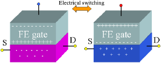
A heterostructure FE field-effect transistor (FE-FET) is basically composed of a FE oxide film and a thin metallic or semiconducting oxide film, as sketched in Fig. 1, similarly to traditional FETs used in the semiconductor industry. In those standard FET devices, the conductivity of the semiconducting channel can be switched on and off by tuning the gate voltage. The FE-FETs can provide similar functions by switching the direction of the polarization of the FE gate. Moreover, this switching, at least ideally, can be non-volatile due to the remnant FE polarization.Ahn et al. (1995); Hoffman et al. (2010) Furthermore, due to the strongly correlated character of the electronic component in several oxides, the above mentioned switching in FE-FET is not limited to the conductivity, but it may also influence on other physical quantities as well, such as the magnetization, orbital order, elastic distortions, etc. Therefore, compared with traditional semiconductor FETs, the physics in FE-FETs can be richer, and potentially additional functionalities can be expected.
Although the FE-FETs have been experimentally studied for several years, only recently theoretical investigations have been focused on this topic.Rondinelli et al. (2008); Duan et al. (2008); Burton and Tsymbal (2009, 2011); Stengel (2011); Bristowe et al. (2011) These recent theoretical studies have been based on the density functional theory (DFT). In fact, studies using model Hamiltonians including strongly correlated electronic effects, beyond the reach of DFT, and focusing on the basic aspects of the FE field effect in these oxide heterostructures are rare. An important technical problem in this context is how to take into account the contribution from the FE polarization on the physics of the microscopic model Hamiltonian representing the other components. In recent efforts by some of us, the FE polarization was modeled as an interfacial potential at the first layer of the conducting channel,Calderón et al. (2011) but this approximation must be refined to address the subtle energy balances between competing tendencies near the interface. Thus, for all these reasons in this manuscript the FE-FET structures will be revisited using model Hamiltonian techniques and applying new approximations to handle this problem. Our effort has the main merit of paving the way for the use of models for the study of FE-FET systems where one of the components has a strongly correlated electronic character that is difficult to study via ab-initio methods.
II Model and method
II.1 Model Hamiltonian
As discussed in the Introduction, in this manuscript the FE field effect will be studied from the model Hamiltonian perspective. More specifically, here the standard two-orbital (2O) double-exchange (DE) model will be used for the metallic component of the heterostructure. This 2O DE model is well known to be successful in modeling the perovskite manganites,Dagotto et al. (2001); Dagotto (2002, 2005a) which are materials often used in FE-FET devices. Furthermore, previous model Hamiltonian studies have already confirmed that the 2O DE model, with some simple modifications, is still a proper model to use for manganite layers when they are in the geometry of a heterostructure.Dong et al. (2008); Brey (2007); Yu et al. (2009); Calderón et al. (2008); Nanda and Satpathy (2008); Calderón et al. (2011) In addition, since the DE mechanism provides a generic framework to describe the motion of electrons in several magnetic systems, the approach followed here, with minor modifications, could potentially be adapted to other oxides beyond the manganites.
As a widely accepted simplification, the limit of an infinite Hund coupling will be adopted in the DE model studied here. Then, more specifically the model Hamiltonian of the metallic channel reads as:
| (1) | |||||
In this expression the first term is the standard DE interaction. The operator () annihilates (creates) an electron at the orbital of the band and at the lattice site , with its spin perfectly parallel to the localized spin . The indexes and represent nearest-neighbor (NN) lattice sites. The Berry phase factor , generated by the infinite Hund coupling limit adopted here, equals , where and are the polar and azimuthal angles defining the direction of the spins, respectively. When a ferromagnetic (FM) background is used, then . The labels and denote the two Mn -orbitals () and (). The NN hopping direction is denoted by . The DE hopping depends on the direction in which the hopping occurs, and it is orbital-dependent as well. The actual hopping amplitudes are:
| (6) | |||||
| (11) | |||||
| (16) |
where is the DE hopping amplitude scale. In the rest of this publication, is considered the unit of energy. Its real value is approximately eV in wide-bandwidth manganites such as La0.7Sr0.3MnO3 (LSMO).Dagotto (2002); Dagotto et al. (2001)
The second term in the Hamiltonian is the on-site potential energy: is the actual potential at each site and is the electronic density operator at the same site. The last term is the Heisenberg-type antiferromagnetic (AFM) superexchange (SE) interaction between the localized NN spins. Its actual typical strength is about that of .Dagotto et al. (2001); Dagotto (2002)
II.2 Self-consistent calculations
In the actual calculations described in this publication, a cuboid lattice (, ==, =) will be used, with open boundary conditions (OBCs) along the -axis to avoid having two interfaces.Yu et al. (2009); Calderón et al. (2011) Twisted boundary conditions (TBCs) are adopted in the - plane to reduce finite size effects, via a -mesh.
The FE gate will be here modeled as a surface charge ( per site, in units of the elementary charge , and located at =) coupled to the first channel layer (=). This approximation has been successfully confirmed in previous DFT calculations.Rondinelli et al. (2008); Duan et al. (2008); Burton and Tsymbal (2009, 2011); Stengel (2011); Bristowe et al. (2011) The long-range Coulomb interaction is included via a layer-dependent potential ,Stengel (2011) and within each layer the potential is assumed to be uniform for simplicity. This electrostatic potential is determined via the Poisson equation.Brey (2007); Yu et al. (2009); Calderón et al. (2008); Nanda and Satpathy (2008); Calderón et al. (2011) In particular, the electric field between the -th and ()-th layers is determined by the net charge [ counted from the FE interface, where is the electronic density corresponding to the -th layer, and is the background (positive) charge density. Thus, the electrostatic potential (with respect to the negative charge of electrons) of each layer can be calculated via the relation:
| (17) |
where is the Coulomb coefficient which is inversely proportion to the dielectric constant [), where is the lattice constant, is the dielectric constant, and is in unit of eVs as explained before]. In the following, is fixed at the value since typical manganites are FM metals at this doping value, e.g. LSMO and La0.7Ca0.3MnO3 (LCMO).Tokura (2006)
In our computational study, the -th layer is assumed to be sufficiently far from the interface such that is set to be as the reference point of the electrostatic potential. This choice, combined with a fixed chemical potential, restores the system to its original bulk state for layers far from the interface. A FM background is adopted to simulate the metallic channel in the FE-FET device. The DE Hamiltonian (including the term with ) is diagonalized to obtain the charge distribution , which is iterated together with until a self-consistent solution is reached. After convergence in and , the total grand potential (per u.c.) can be calculated as:
| (18) | |||||
where is the fermionic grand potential (per site), calculated from the diagonalization eigenvalues. The second term considers the reduction of the electrostatic Coulomb energy of the electrons, since it is doubly-counted in the first term. The third and fourth terms are the electrostatic Coulombic energies of the positive background charge () and the FE surface charge, respectively. The last term describes the AFM SE energy, namely the Heisenberg interaction among the localized spins. A finite but low temperature = ( K) is used for the Fermi-Dirac distribution function smearing.
III Results and Discussion
III.1 Charge accumulation/depletion
To investigate the screening effects in the FE-FET heterostructure, the results for four values of (, , , and ) were compared. For each , the surface charge is initially set to zero to find the chemical potential where the average density equals . With this chemical potential, is then varied from to (in units of the elementary charge per cell). Ideally, = corresponds to a FE polarization as large as C/cm2 (if the pseudocubic lattice constant is set as Å), which is a typical and reasonable value for standard FE oxide materials.
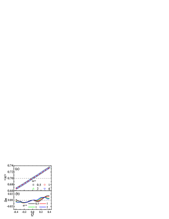
The screening effects correspond to the accumulation/depletion of charges near the interface. Under a positive (negative) , more electrons will be attracted to (repelled from) the interface. Since the chemical potential is fixed in our simulation, the screening effect can also be obtained from the average density as a function of , as shown in Fig. 2. This screening effect increases when is increased, which is concomitant with a stronger electrostatic Coulomb interaction near the interface. In the rest of the manuscript, = will be here adopted: using = eV and = Å, this value corresponds to a relative permittivity , which is quite reasonable to represent real materials. Also note that = is already very close to the fully screened case according to the results shown before. It should be remarked that the total charge for the whole system is zero (i.e. the combined FE gate and manganite channel are neutral) although the gate and channel themselves are charge polarized.
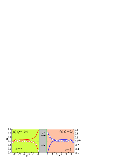
The screening effect is better observed by studying the electron density profiles and their corresponding electrostatic potentials in Fig. 3. The = and cases are shown together for better comparison. When =, then becomes deep enough near the interface to accumulate considerably more electrons than in the bulk. In contrast, when =, then is large and positive near the interface, thus repelling those electrons. With =, the screening of electrons is the most significant within a thin region near the interface, typically involving just layers for the 2O DE model employed here.
III.2 Interfacial phase transitions
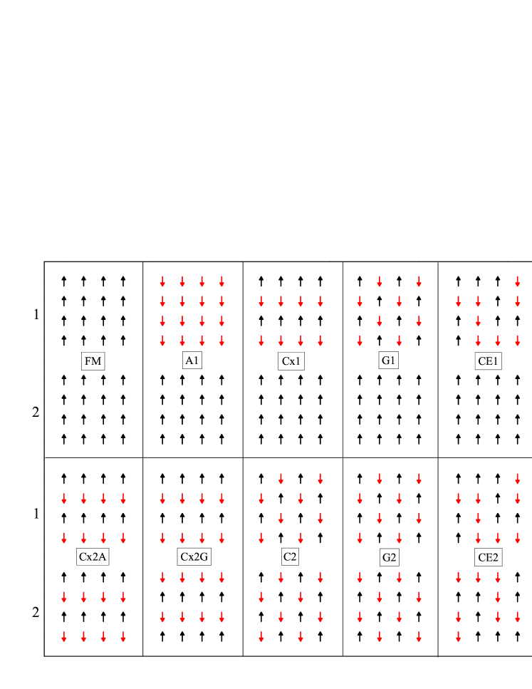
Since the previous results show that the interfacial electronic density can be substantially modulated by the FE polarization, then it is natural to expect local phase transitions. The reason is that the phase diagrams of oxides are usually highly sensitive to charge density variations,Dagotto (2005b) i.e. density-driven phase transitions are well known to occur in bulk materials when chemically doped to modify the electronic density.Burton and Tsymbal (2009, 2011) To explore these possible phase transitions, the zero-temperature variational method is here employed by comparing the total ground-state energy (Eq. 18) for a variety of spin patterns. From Fig. 3, it is clear that most of the charge accumulation/depletion occurs within the first two layers near the FE interface. Hence, for simplicity the several non-FM (collinear) spin patterns explored here will only be proposed to exist in these two layers in our present variational calculation, while the spins in the other layers remain fixed to be FM. The candidate spin patterns in the two interfacial layers are shown in Fig. 4.
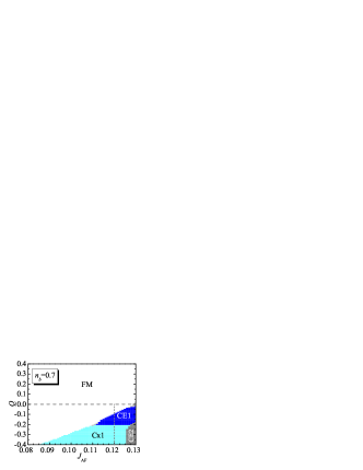
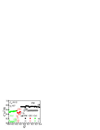
The ground state phase diagram obtained in our calculations for the interfacial layers in FE-FET is shown in Fig. 5. According to this phase diagram, the original FM metallic phase at = is stable when , while the boundary between the FM and A-type AFM phases is at = for the calculation representing the bulk (see Fig. 7 later in this publication). These two almost identical values suggest that the lattice size effects and surface effects are negligible in our simulation of FE-FET.
By adjusting the FE polarization (i.e. by modifying the surface charge ) in the FE-FET setup, in the present variational effort it has been observed that the interfacial spins have a transition to arrangements different from the original FM state. This is the main result of our publication. For example, the CE1 and Cx1 orders are stabilized and replace the FM state in sequence with increasing negative when , as shown in Fig. 5. In contrast, the FM order remains robust under a positive , thus establishing an asymmetry in the response of the system to the FE polarization orientation that is of value for applications.
The FE screening effect plays an important role to determine the dominant interfacial spin order, that is competing with the DE mechanism that favor ferromagnetism. Considering = as example, when the CE1 and Cx1 orders can accommodate more holes near the interface than the original FM state, thus reducing the Coulomb potential pronouncedly, as shown in Fig. 6. In simple words, the system chooses an interfacial state which can screen the FE polarization rather well.
III.3 Comparison with bulk properties
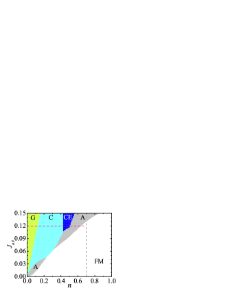
For comparison, the ground state of the bulk is also calculated using the standard 2O DE model, under a similar variational approximation with states now covering the whole system. This information can be used as a guide to explore the interfacial spin orders that may be of relevance in the FE-FET setup. The results are shown in Fig. 7. Considering the simplicity of the model (with only two competing NN interactions: DE vs SE), this phase diagram agrees fairly well with the experimental perovskite manganite results.Tokura (2006) The most typical phases found in bulk manganites, namely the FM and various AFM states (A-, C-, G-, and CE types), appear in the proper density and bandwidth regions, providing support to the qualitative accuracy of our calculations.
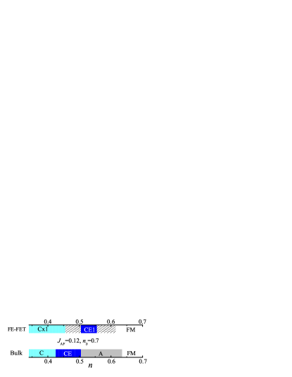
Considering = as an example, Fig. 8 compares the spin order transitions in the bulk and in the FE-FET. In the bulk’s phase diagram, by reducing the density from =, the system transitions from a FM phase to an A-type AFM state at =, then from A to CE at =, and from CE to C-type AFM one at =. In the FE heterostructure, on the other hand, the system changes from FM to CE1 at = (= in FM and = in CE1), and then from CE1 to Cx1 at = (= in CE1 and = in Cx1). There are several interesting aspects in this interfacial phase transitions. First, the “critical” densities are found to be different between the bulk and the FE-FET heterostructure. Second, the fragile A-type AFM state is absent in the heterostructure geometry. Third, in the heterostructure the interfacial electronic density jumps at the locations of the spin order transitions, causing some density regions to be unreachable (i.e. they are unstable). Such density discontinuities originate from the well-known electronic phase separation tendencies in manganites,Dagotto et al. (2001); Dagotto (2002, 2005a) a phenomenon that does not have an analog in semiconducting devices. Last but not least, the CE1 and Cx1 states predicted here have not been considered in previous DFT studies, since these states typically need larger in-plane cells than previously analyzed with DFT. These two interfacial states, CE1 and Cx1, may exist particularly in those manganite channels with relative narrow bandwidths, such as LCMO.
There are two main reasons for the differences observed here in the phase diagrams between the bulk and the heterostructures. The first reason is the FE screening effect, as shown in Fig. 6, namely the ground state near the interface is determined not only by the competition between the DE kinetic energy and the SE energy as in the bulk, but also by the electrostatic potential energy. Second, since the spin order transitions occur only near the interface, the global phases shown here, except for the FM one, are actually “artificial” phase separated states involving a combination of the bulk and the interfacial states, combination that may be more stable than the homogeneous spin orders in the FE-FETs. Thus, these examples show that it is not enough to simply guess the interfacial spin orders from those in the bulk phase diagrams with only homogeneous phases: new states may emerge at the interfaces.
Furthermore, it should be noted that these phase transitions may be even more complex than our calculations suggest. For instance, other states beyond the candidates considered here, for instance involving canted spins and thicker interfacial layers, may become stable in some regions. To reveal additional details of these interfacial phase transitions, unbiased (and very CPU time consuming) studies involving Monte Carlo simulations should be performed in the future, including electron-phonon couplings and finite temperature effects. However, the results discussed here are already sufficient to clearly show that the original FM phase is indeed unstable toward other phases at the interface with a FE, which was the main goal of this publication.
III.4 Spin flip vs spin rotation
Although the studies described above already clearly show that interfacial phase transitions away from the FM state will occur by tuning the FE polarization, the fine details of these phase transitions remain unclear. Do these spins flip abruptly from one configuration to the other or do they rotate gradually upon increasing ? Are there any canted spin states tendencies besides the collinear spin candidates considered here? Reaching a full answer to these questions is computationally very difficult at the current state of typical Monte Carlo simulations with an effort that grows like the fourth power of the number of sites . However, some studies concerning spin rotation vs. spin flip tendencies can still be carried out in a variational manner, as described below.
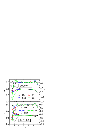
As shown in Fig. 5, the FM order turns into the CE1 order upon increasing , which involves only one interfacial layers. During this transition, half of the spins in the first layer flip to “down” spins in the final CE1 state. For simplicity, let us assume that this phase transition (spin flip) occurs via an in-plane spin rotation. To reach the CE1 order, the spins in the first layers are partitioned into CE type zigzag chains. Half of those zigzag chains are assumed to rotate synchronously, namely they are characterized by an unique spin angle . Using the variational method, can be determined as a function of , as shown in Fig. 9. Since the phase boundary between the FM and CE1 states also depends on the SE coupling (), the spin flip/rotation process varies with . For all sets of shown here, the “speeds” of the spin rotations are not uniform. Note that a sharp jump of always exists in each of the curves. There are only a few spin canted states that are stable as intermediate states during the spin rotation process, most of which exist near the FM side (i.e. ). Thus, the spin canting process does not seem to be very robust, at least according to our qualitative calculations. Instead, a sudden spin flip may be the preferred process for the interfacial phase transitions.
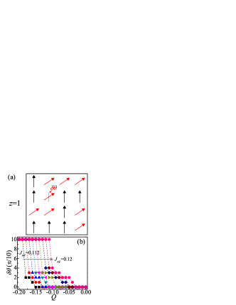
A better characterization of the spin flip vs. spin rotation tendencies relates with the first-order vs. second-order transition character of the process. From Fig. 9, it seems that both spin flip and spin rotation are allowed. However, the canting angles ’s are restricted near in the spin flip case. Thus, there seems to occur a first-order transition between a FM-like state (with ) and an AFM state (with ). Of course, more powerful unbiased computational methods should be used to confirm this conclusion.
III.5 Resistive switching
Although the charge accumulation/depletion and associated local phase transitions induced by the switch of the FE polarization orientation occur only near the interface, these transitions lead to a global change in the conductance of the metallic channel (e.g. LSMO) when the FE polarization is flipped. This resistive switch effect should be bipolar, due to the asymmetric phase diagram found in our calculations, as shown in Fig. 5. This effect should also be anisotropic, because in a metallic channel, when the interfacial layers become less conducting due to the previously described phase transitions, the out-of-plane conductance will be seriously suppressed basically due to the spin valve effect Burton and Tsymbal (2011); Bristowe et al. (2011) while the in-plane transport will be only weakly affected, as shown in Fig. 10. It should be noted that here a good FM metallic channel is used, while more prominent resistive changes are expected to occur in those systems which are close to metal-insulator phase boundaries.
Besides the changes of the resistivity, magnetoelectric effects have also been observed in experimentally studied FE-FET heterostructures.Molegraaf et al. (2009); Vaz et al. (2010a, b) Qualitatively, the change of the magnetization can be understood via the local phase transitions near the interface when the FE polarization is flipped (Fig. 6 and Fig. 9), as described in this manuscript.
Finally, it should also be noted that our current effort provides just a starting point to study the FE field-effect heterostructures with the use of model Hamiltonians. Additional realistic effects in real heterostructures were neglected in the present work, such as lattice structural distortions and chemical bonding effects. Thus, the current predictions may be not as accurate as those reached with DFT calculations for some particular materials. The main relevance of the present model-based study is that it can provide overall tendencies for a material family. The study of the effect of more realistic interactions and the inclusion of finite-temperature effects can be achieved in future calculations based on the model described here.
IV Conclusions
In summary, a microscopic model Hamiltonian for the FE oxide - FM metallic oxide heterostructures, a prototypical FE-FET system, has been here studied. The FE field effect is modeled via the electrostatic Coulomb potential in the FM oxide. Using a self-consistent calculation and the variational method, an interfacial charge accumulation/depletion is found by tuning the magnitude and sign of the FE polarization. Phase transitions at the interface have been observed here by modulating the electronic charge density of the metallic component by varying the FE polarization. Our present effort provides a starting point to study the FE field effect via model Hamiltonians. Our results clearly present some common similarities with previous DFT effort, confirming their main results. However, the framework is conceptually different and the results reported here are not identical to those of DFT. Moreover, our model is generic and it can be adapted to study a variety of other oxide heterostructures involving ferroelectrics, particularly those where the metallic component has a strongly correlated electronic character.
V Acknowledgments
We thank Ho Nyung Lee for helpful discussions. The work of S.D. was supported by the 973 Projects of China (2011CB922101, 2009CB623303), NSFC (11004027), and NCET (10-0325). R.Y. was supported by the NSF grant (DMR-1006985) and the Robert A. Welch Foundation (C-1411). X.Z. and E.D. were supported by the U.S. Department of Energy, Office of Basic Energy Sciences, Materials Science and Engineering Division.
References
- Dagotto (2007) E. Dagotto, Science 318, 1076 (2007).
- Takagi and Hwang (2010) H. Takagi and H. Y. Hwang, Science 327, 1601 (2010).
- Mannhart and Schlom (2010) J. Mannhart and D. G. Schlom, Science 327, 1607 (2010).
- Hammerl and Spaldin (2011) G. Hammerl and N. Spaldin, Science 332, 922 (2011).
- Ramesh and Spaldin (2007) R. Ramesh and N. A. Spaldin, Nature Mater. 6, 21 (2007).
- Bibes et al. (2011) M. Bibes, J. E. Villegas, and A. Barthélémy, Adv. Phys. 60, 5 (2011).
- Nan et al. (2008) C.-W. Nan, M. I. Bichurin, S. X. Dong, D. Viehland, and G. Srinivasan, J. Appl. Phys. 103, 031101 (2008).
- Wu et al. (2010) S. W. Wu, S. A. Cybart, P. Yu, M. D. Rossell, J. X. Zhang, R. Ramesh, and R. C. Dynes, Nature Mater. 9, 756 (2010).
- Yu et al. (2010) P. Yu, J.-S. Lee, S. Okamoto, M. D. Rossell, M. Huijben, C.-H. Yang, Q. He, J. X. Zhang, S. Yang, M. J. Lee, Q. M. Ramasse, R. Erni, Y.-H. Chu, D. A. Arena, C.-C. Kao, L. Martin, and R. Ramesh, Phys. Rev. Lett. 105, 027201 (2010).
- Dong et al. (2009) S. Dong, K. Yamauchi, S. Yunoki, R. Yu, S. Liang, A. Moreo, J.-M. Liu, S. Picozzi, and E. Dagotto, Phys. Rev. Lett. 103, 127201 (2009).
- Belashchenko (2010) K. D. Belashchenko, Phys. Rev. Lett. 105, 147204 (2010).
- Livesey (2010) K. L. Livesey, Phys. Rev. B 82, 064408 (2010).
- Okamoto (2010) S. Okamoto, Phys. Rev. Lett. 82, 024427 (2010).
- Zheng et al. (2006) R. K. Zheng, J. Wang, X. Y. Zhou, Y. Wang, H. L. W. Chan, C. L. Choy, and H. S. Luo, J. Appl. Phys. 99, 123714 (2006).
- Zheng et al. (2009) R. K. Zheng, H.-U. Habermeier, H. L. W. Chan, C. L. Choy, and H. S. Luo, Phys. Rev. B 80, 104433 (2009).
- Guo et al. (2011) E. J. Guo, J. Gao, and H. B. Lu, Appl. Phys. Lett. 98, 081903 (2011).
- Rondinelli et al. (2008) J. M. Rondinelli, M. Stengel, and N. A. Spaldin, Nature Nano. 3, 46 (2008).
- Duan et al. (2008) C.-G. Duan, J. P. Velev, R. F. Sabirianov, Z. Zhu, J. Chu, S. S. Jaswal, and E. Y. Tsymbal, Phys. Rev. Lett. 101, 137201 (2008).
- Ahn et al. (1995) C. H. Ahn, J.-M. Triscone, N. Archibald, M. Decroux, R. H. Hammond, T. H. Geballe, Ø. Fischer, and M. R. Beasley, Science 269, 373 (1995).
- Mathews et al. (1997) S. Mathews, R. Ramesh, T. Venkatesan, and J. Benedetto, Science 276, 238 (1997).
- Hoffman et al. (2010) J. Hoffman, X. Pan, J. W. Reiner, F. J. Walker, J. P. Han, C. H. Ahn, and T. P. Ma, Adv. Mater. 22, 2957 (2010).
- Molegraaf et al. (2009) H. J. A. Molegraaf, J. Hoffman, C. A. F. Vaz, S. Gariglio, D. van der Marel, C. H. Ahn, and J.-M. Triscone, Adv. Mater. 21, 3470 (2009).
- Vaz et al. (2010a) C. A. F. Vaz, J. Hoffman, Y. Segal, J. W. Reiner, R. D. Grober, Z. Zhang, C. H. Ahn, and F. J. Walker, Phys. Rev. Lett. 104, 127202 (2010a).
- Vaz et al. (2010b) C. A. F. Vaz, Y. Segal, J. Hoffman, R. D. Grober, F. J. Walker, and C. H. Ahn, Appl. Phys. Lett. 97, 042506 (2010b).
- Hong et al. (2005) X. Hong, A. Posadas, and C. H. Ahn, Appl. Phys. Lett. 86, 142501 (2005).
- Zhao et al. (2004) T. Zhao, S. B. Ogale, S. R. Shinde, R. Ramesh, R. Droopad, J. Yu, K. Eisenbeiser, and J. Misewich, Appl. Phys. Lett. 84, 750 (2004).
- Thiele et al. (2005) C. Thiele, K. Dörr, L. Schultz, E. Beyreuther, and W.-M. Lin, Appl. Phys. Lett. 87, 162512 (2005).
- Chaudhuri et al. (2007) A. R. Chaudhuri, R. Ranjith, S. B. Krupanidhi, R. V. K. Mangalam, and A. Sundaresan, Appl. Phys. Lett. 90, 122902 (2007).
- Watanabe (1995) Y. Watanabe, Appl. Phys. Lett. 66, 1770 (1995).
- Kuffer et al. (2005) O. Kuffer, I. Maggio-Aprile, and Ø. Fischer, Nature Mater. 4, 378 (2005).
- Eblen-Zayas et al. (2005) M. Eblen-Zayas, A. Bhattacharya, N. E. Staley, A. L. Kobrinskii, and A. M. Goldman, Phys. Rev. Lett. 94, 037204 (2005).
- Burton and Tsymbal (2009) J. D. Burton and E. Y. Tsymbal, Phys. Rev. B 80, 174406 (2009).
- Burton and Tsymbal (2011) J. D. Burton and E. Y. Tsymbal, Phys. Rev. Lett. 106, 157203 (2011).
- Stengel (2011) M. Stengel, Phys. Rev. Lett. 106, 136803 (2011).
- Bristowe et al. (2011) N. C. Bristowe, M. Stengel, P. B. Littlewood, J. M. Pruneda, and E. Artacho, arXiv: , 1108.2208 (2011).
- Calderón et al. (2011) M. J. Calderón, S. Liang, R. Yu, J. Salafranca, S. Dong, a. L. B. S. Yunoki, A. Moreo, and E. Dagotto, Phys. Rev. B 84, 024422 (2011).
- Dagotto et al. (2001) E. Dagotto, T. Hotta, and A. Moreo, Phys. Rep. 344, 1 (2001).
- Dagotto (2002) E. Dagotto, Nanoscale Phase Separation and Colossal Magnetoresistance (Berlin: Springer, 2002).
- Dagotto (2005a) E. Dagotto, New J. Phys. 7, 67 (2005a).
- Dong et al. (2008) S. Dong, R. Yu, S. Yunoki, G. Alvarez, J.-M. Liu, and E. Dagotto, Phys. Rev. B 78, 201102(R) (2008).
- Brey (2007) L. Brey, Phys. Rev. B 75, 104423 (2007).
- Yu et al. (2009) R. Yu, S. Yunoki, S. Dong, and E. Dagotto, Phys. Rev. B 80, 125115 (2009).
- Calderón et al. (2008) M. J. Calderón, J. Salafranca, and L. Brey, Phys. Rev. B 78, 024415 (2008).
- Nanda and Satpathy (2008) B. R. K. Nanda and S. Satpathy, Phys. Rev. B 78, 054427 (2008).
- Tokura (2006) Y. Tokura, Rep. Prog. Phys. 69, 797 (2006).
- Chisholm et al. (2010) M. F. Chisholm, W. Luo, M. P. Oxley, S. T. Pantelides, and H. N. Lee, Phys. Rev. Lett. 105, 197602 (2010).
- Dagotto (2005b) E. Dagotto, Science 309, 257 (2005b).
- Vergés (1999) J. A. Vergés, Comput. Phys. Commun. 118, 71 (1999).