Pseudo-potential Band Structure Calculation of InSb Ultra-thin Films and its application to assess the n-Metal-Oxide-Semiconductor Transistor Performance
Abstract
Band structure of InSb thin films with surface orientation is calculated using empirical pseudopotential method (EPM) to evaluate the performance of nanoscale devices using InSb substrate. Contrary to the predictions by simple effective mass approximation methods (EMA), our calculation reveals that valley is still the lowest lying conduction valley. Based on EPM calculations, we obtained the important electronic structure and transport parameters, such as effective mass and valley energy minimum, of InSb thin film as a function of film thickness. Our calculations reveal that the ’effective mass’ of valley electrons increases with the scaling down of the film thickness. We also provide an assessment of nanoscale InSb thin film devices using Non-Equilibrium Green’s Function under the effective mass framework in the ballistic regime.
pacs:
73.40.Gk, 73.40.Rw, 75.70.CnI Introduction
Ultra-thin body (UTB) metal-oxide-semiconductor-field-effect-transistor (MOSFET) structure is a promising candidate for scaling MOSFET devices into the nanometer regime because it has the excellent attribute of suppressing various short channel effects caused by the downscaling of device gate length itrs . Recently, there are also experimental and theoretical efforts to evaluate use of non-conventional channel orientation yu ; komoda ; low or new channel materials (such as Ge, III-V compound semiconductors, due to their small -valley electron masses) low ; fischetti ; ashley to improve the MOSFET performance.
In particular, InSb is being considered as a new channel material ashley for state-of-the-art MOSFET devices because of its high bulk mobility (in fact, it has the highest electron and hole mobility among common III-V semiconductors mfli ; lev ). Theoretical investigation of InSb MOSFET devices based on a simple effective mass approximation (EMA) had been conducted in pethe to predict its device performance limits . It was predicted that the -valley energy rises rapidly under body quantization and the inversion charges in the thin film are transferred to the L-valley. Therefore the advantage of the high injection velocity from the -valley electrons is lost. Work in pethe used bulk effective mass even in thin film regime. However, EMA may not be a reliable method in describing the electronic band structure of thin films due to unaccounted effects like band coupling and non-parabolic dispersion. We also found that the bulk effective mass can only describe the energy dispersion in a very small range of k space, which brings to question how accurately EMA can capture the quantization effect in thin film (see the discussions on Fig. 7 in this paper).
In this work, we describe a more physically reliable and accurate model, the local empirical pseudopotential method (EPM)harrison ; heine , to study InSb thin films. Our results show that the charge transfer from the to the L valley does not occur and the effective masses in transverse directions become larger than those in bulk material, which have a direct impact on the device transport properties. This paper serves to communicate in detail the models employed in our published conference paper zhu . In section II, we give a detailed description of the theoretical background of EPM. We will discuss introduction of a model potential to describe the atomic pseudopotential, which allows us to extend EPM to thin film calculations. In subsection II. B, we derive the spin-orbit coupling contribution to the matrix element of the Hamiltonian used in EPM calculation. In order to achieve accurate results in EPM calculations of thin film band structures, we introduce two parameters to take account into the volume renormalization and the spin-orbit coupling. In subsection II. C, we discuss the methodology adopted to passivate the surface dangling bonds by using Hydrogen (H) atom bonding. In section III, we discuss the important features of InSb thin film electronic structure. We also obtained important electronic parameters, such as effective mass and valley energy minimum, of InSb thin film as a function of film thickness. In section IV, we provide an assessment of nanoscale InSb thin film double-gated MOSFET devices using non-equilibrium Green’s Function under the effective mass framework in the ballistic regime derived from realistic thin film band structure reported in this paper. Finally, we give conclusions in section V.
II Theoretical Background
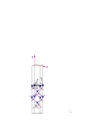
The EPM has already been successfully applied in band structure calculations of metal, semiconductor or other materials fong ; cohen ; cohen1 . It has also been extended to calculate band structures and electronic properties of Si quantum dots wang ; wang1 , quantum wires xia ; yeh , and quantum films xia1 ; sbzhang . In view of pedagogical clarity, we shall also give an overview of the essential theoretical aspects of EPM. Before going into the rigorous mathematical details, we shall first give an overall description of the method used in this work. The key aspects of applying the EPM to a thin film calculation are as follows; (1) a supercell (Fig. 1) has to be specified prior to any calculation. A sufficiently large vacuum layer has to be explicitly included in the supercell so as to eliminate any wavefunction overlap between different thin film layers. (2) We have to determine the suitable atomic pseudopotentials for the Sb and In atoms independently for our thin film calculations. (3) The effect of spin-orbit coupling needs to be included because it is sufficiently large to affect the band structure significantly (see Table III) in InSb and many other compound semiconductors. (4) Hydrogen passivation of the surface dangling bonds is incorporated into model potential. This is very crucial treatment as the surface dangling bonds will lead to surface states in the band gap which will overwhelm the band structure of the thin film, especially in small band gap materials like InSb. Therefore we would also need to determine the pseudopotential of Hydrogen atoms.
II.1 Pseudopotential Method
II.1.1 Empirical Pseudopotential of Bulk InSb
It is well-known that the band structure can be derived by solving a secular equation mfli . The matrix element of the pseudopotential (PS) is
| (1) |
where
| (2) |
is the volume of the unit cell, is the number of unit cells, and are reciprocal lattice vectors, is the form factor, and is the plane wave basis function. In a single crystal, there are usually several basis atoms associated with each lattice point located at a position in a unit cell. These atoms have relative positions from the lattice point at . The summation over will yield us the atomic configuration information of the unit cell. Note that, the bold letters and the letters with an overhead arrow denote vectors throughout this paper.
| Form factor (Ry) | |||||||
|---|---|---|---|---|---|---|---|
| ESAFF | -0.858 | -0.20 | 0 | 0.018 | 0.034 | 0 | |
| 0 | 0.035 | 0.032 | 0 | 0.011 | 0.013 | ||
| EMP | -0.816 | -0.202 | 0 | 0.0179 | 0.03416 | 0 | |
| 0 | 0.0353 | 0.0312 | 0 | 0.01221 | 0.0114 | ||
Before we proceed with the calculation of InSb thin film band structure, we need to derive the atomic pseudopotential (PS) of In and Sb atoms respectively, or more accurately speaking, to construct an empirical PS. We can obtain important information about the atomic PS from bulk InSb band structure, since its calculated band structure can reliably be calibrated against experimental data. For bulk InSb, there are two atoms in a unit cell. Conventionally, bulk empirical PS (at special values, they are also known as Empirical Symmetry and Anti-symmetry Form Factors (ESAFF), as shown in Table I) can be defined as the summation and the difference of the individual atomic PSs of Sb and In. The symmetry and anti-symmetry structure factors are given respectively, as and , where . It should be noted that if we define the symmetry and anti-symmetry form factors for InSb as and , then the factor appearing in Eq.(2) will be , where is the atomic volume in a unit cell.
By performing EPM calculation of the bulk band structure iteratively, a suitable set of ESAFF is obtained such that it yields the ’correct’ energy gaps at pertinent symmetry points mfli ; lev . This set of ESAFF is shown in Table I. Because of the spherical symmetry approximation of the local pseudopotential, the first few lowest energy shells are at normalized equal to 3, 4, 8, 11 and 12, where is wave vector in unit and is crystal lattice constant. Based on this set of ESAFF, we can devise a suitable interpolation scheme that allows us to reasonably predict a pseudopotential value at other values. This will then allow us to extend this EPM method to calculation of thin film band structure of arbitrary thickness. An essential assumption we are invoking is that the atomic pseudopotential is transferable and thus will not be changed from the bulk to a thin film. This assumption is reasonable because ab initio calculation has demonstrated that the bulk potential will just be changed in only one atomic layer at the interface for GaAs/AlAs superlattice vande and will be exactly the same for all other atoms. Hence, the potential will be bulk-like potential except at one atomic layer at the surface of the thin film. Therefore, the bulk atomic potential can be used in thin film calculation. However, further investigation reveals that we must add the renormalization factor to the pseudopotential to give the correct results for thin film as shown in the subsection II. A. 2.
II.1.2 Thin Film and Empirical Model Potential (EMP)
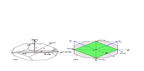
For surface InSb thin film band structure calculation, we use a supercell as shown in Fig. 1. Fig. (2a) depicts the first Brillouin zone of bulk InSb and its subsequent projection onto the xy plane, i.e. the first Brillouin zone of InSb thin film in 2D, is shown in Fig. (2b). In this paper, band structure of InSb thin film will be plotted using the same coordinate system for 2D reciprocal vector space as illustrated in Fig. (2b).
In bulk InSb, band structure is determined by the pseudopotential at several values as stated in previous section and the shells with are not of much importance. For thin film InSb, the reciprocal primitive vector will be shorter than that of bulk and thus the radius of the lowest energy shell is smaller. This is the consequence of a larger primitive vector in real space in direction for film (see Fig. 1). Therefore, the shells with are also very important for band structure calculation and their effects must be properly predicted and included in our calculation. To account for them, we shall employ an empirical model potential that can give the continuous pseudopotential as a function of . We use a model potential wang ; wang1 ; yeh ; sbzhang
| (3) |
where the subscript ”atom” is used to distinguish the different atomic species’ pseudopotential. , , and are fitting parameters such that they yield the correct form factor as determined by ESAFF.
| Parameters | Sb | In |
|---|---|---|
| 0.2588 | 719470 | |
| 1.5832 | 2.0811 | |
| 1.9689 | 3813600 | |
| 0.7159 | 0.9116 |
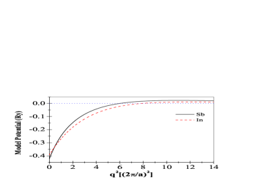
To obtain a unique atomic model potential of In and Sb, we need eight constraints for the eight fitting parameters. Seven constraints come from the seven nonzero ESAFF parameters at equal to 3, 4, 8, 11 and 12 shown in Table I. The remaining one constraint is imposed by InSb work function (WF), which gives one nonzero ESAFF at equal to 0 sbzhang . This last constraint accounts for the surface property, which is important for a thin film sbzhang . In fitting these parameters, it should be noted that the physical unit of in Eq. (3) is and is in rydberg atomic unit. The best fitting parameters for the model potential are shown in Table II and its variation with is shown in Fig. 3. From this figure, we observe that the model potentials of Sb and In atoms are in a reasonable range. Also, the fits to and are quite good as is clear from Table I.
| Energy (eV) | Experiment | Calculation 1 (ESAFF) | Calculation 2 (EMP) |
|---|---|---|---|
| 0.17 | 0.172 | 0.168 | |
| 0.68 | 0.685 | 0.704 | |
| 1.0 | 0.995 | 1.034 | |
| 0.8 | 0.801 | 0.802 | |
| WF | -4.76 | -4.760 | -4.223 |
We perform EPM calculation of bulk InSb using this new model potential and reproduce the required energy band minima derived from experiment, as tabulated in Table III. We shall point out that the model potential of one of the species of an atom in a semiconductor compound is actually atomic model potential, i.e. the volume of unit cell is divided by the number of atoms in this unit cell. So for the thin film calculations, there will be a renormalization with a different unit cell volume under the assumption that the overall pseudopotential of atoms is the superposition of the local pseudopotential of all the atoms in the thin film.
II.2 Hydrogen Passivation
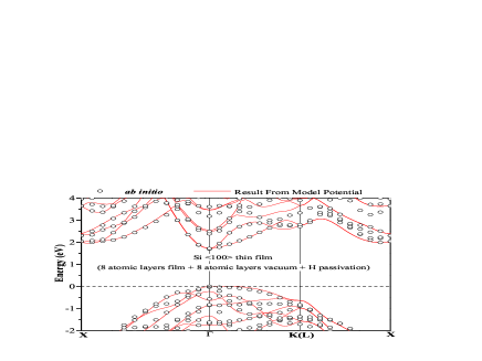
In thin film calculation, we must ensure that surface dangling bonds are correctly passivated with Hydrogen (H) so that there will be no surface states within the band gap. To determine model potential for Hydrogen, we tried model potential of H in wang ; yeh ; sbzhang and calculated the band structure of 8 atomic layers (atm) Si thin film and compared the EPM results with those derived from ab initio calculation segall (Fig. 4). The band structure obtained from both methods are very consistent, thus establishing the validity and reliability of this H model potential. In Si thin film calculation, the renormalization of supercell volume is set as a ratio of the number of H atoms in the supercell and the number of Si atoms in the same unit cell. Also we assumed that the atomic volume of H is the same as that of Si.
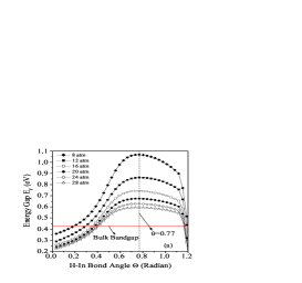
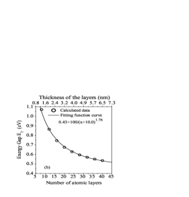
For InSb thin film, the bond length of In-H is set as (from experiment in rag ) and Sb-H as (from ab initio energy minimization calculation segall , which is very close to in Ref. gabor ). The angle between the bond of In-H and the top surface () (Fig. 1), should be determined carefully. Fig. (5a) shows the calculated direct InSb band gap () as a function of for varying number of InSb atomic layers. In principle, the energetically stable for the thin film system is when is stationary with respect to . as a function of shown in Fig. (5a) confirms as a stationary value for and a fitting formula (similar to wang ; yeh ; sbzhang ) affirms that approaches the bulk band gap of eV as the film thickness tends to the bulk limit as shown in Fig. (5b) (without spin-orbit contribution).
For InSb thin film, we need to renormalize Hydrogen atomic potential derived from Si thin film calculation, using relative volume of H atoms compared to the volume of InSb, where and are supercell volumes of Si and InSb respectively. Since the InSb thin film has the same supercell structure as Si thin film, its supercell renomalization is performed using their respective lattice constants as .
II.3 Spin-Orbit Coupling (SOC)
SOC treatment is incorporated by calculating the matrix element of the spin-orbit coupling term in the Hamiltonian expressed in a plane wave representation. It can be reduced to an expression similar as the pseudopotential form factor, known as the spin orbit form factors (SOFFs) weisz ; che ; walter ; bloom . In this section, we will clarify the formulation used for SOC treatment. A more mathematically detailed derivation shall be presented in the Appendix.
If we consider a supercell composed of different species of basis atoms at each lattice site, the spin-orbit Hamiltonian can be specified as
| (4) |
where is a parameter for -th species, is the number of species, is the change in the wave vector, are matrix elements of Pauli matrices, and denote the spin states; up spin or down spin. Structure factor is given as , where the summation is over atoms of -th species (see Appendix for more detail).
The parameters are determined by the function defined in the appendix (see Eq. (23)). The spin-orbit parameter (see Eq. (19)) is a property of isolated atoms, so it is independent of the crystal wave vector. The defined function is important in the calculation of and its behavior is depicted in Fig. 6.
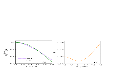
In Fig. 6, we plot the variation of the B function (i.e. Eq. (23)) as a function of wave vector for Sb and In atoms in (a) and the difference of the B function between these two types of atoms in (b). For our plot in Fig. 6, we just show the outermost core state, i.e. and ( orbit). Because of the normalization, the B function tends to 1 as .
Although the explicit form of the spin-orbit coupling matrix element is presented in the Appendix, there are some additional steps that must be taken into consideration in order to obtain the correct result. Thus, we shall briefly elaborate the procedures involved in SOC treatment. First off all, the SOFFs are obtained via a similar methodology as ESAFF; by iterating our EPM calculations until the correct energy gaps are obtained for bulk InSb. SOFFs have to be normalized with respect to supercell volume when used for a thin film calculation. Besides the usual volume renormalization, one has to account for another renormalization. Conventionally, bulk band structure of InSb is derived by considering a 2-atom unit cell in which the primitive vectors are non-orthogonal and the mutual angles between them are all . In thin film calculation, a larger supercell is constructed in which the primitive vectors are mutually orthogonal. Hence this angular effect renormalization and volume renormalization must be considered in our treatment.
The spin orbit Hamiltonian is divided into two parts; one part dealing with the angular part and the other the magnitude part. When the supercell is changed from bulk 2-atom unit cell to thin film supercell, the volume renormalization will appear in the second part like what has been done on form factors of pseudopotential of Sb and In. For the angular part renormalization, we treat it as an unknown parameter which we derived using the following procedure. We removed the vacuum slab from the thin film supercell. This new supercell is therefore a unit cell for a bulk crystal. We then adjust the angular part renormalization parameter so that it reproduces the correct bulk band structure and spin orbit splitting (as calculated from a conventional bulk crystal unit cell). This procedure has to be repeated for each film thickness. After this remormalization, the vacuum slabs are replaced again and the thin film band structure can be derived from EPM.
III Features of InSb Electronic Structures
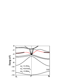
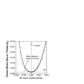
Fig. (7a) shows the calculated band structure of bulk InSb from our EPM. We derived the following effective masses: (the longitudinal mass of L valley), (the longitudinal mass of valley) and (the isotropic mass of valley). The open circles in Fig (7a) are data points fitted to the bands minima by using a parabolic dispersion with effective masses as stated. Fig. (7b) shows the ’effective mass’ in the vicinity of valley () calculated by taking the second derivative of energy with respect to the wave vector . We note that the parabolic assumption for the energy dispersion at is only valid for a very small range. Consider a 1.3 nm InSb film, the wave vector spread according to uncertainty principle is . From the plot, the parabolic assumption for EMA is only applicable up to a range of . Hence, in the ultra thin film regime, a parabolic EMA is not a reasonable assumption and becomes a highly unreliable method for calculation of size quantization effect. In addition, the small band gap also entails a considerable amount of coupling between the conduction and valence bands, which render the uncoupled EMA approach unreliable.
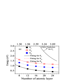
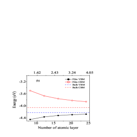
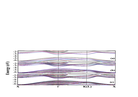
Fig. 8 shows the calculated band structure of thin film InSb from our EPM. These thin films still retain the direct band gap properties in contrast to EMA calculation pethe , which has valley as the lowest lying conduction valley when film thickness is below 5 nm. Fig. (9a) shows variation of the energy minima at and valleys as function of film thickness. We also plot the fitting curves for the energy minima as a function of thickness x in this figure. The fitting formulas are , , and , respectively. There was no crossing of the energy minima down to 6 atomic layers, in contrast to predictions by EMA methods. In addition, we note that the lowest lying valley is separated from the other valleys with a gap more than eV, signifying that electrons are dominantly occupying valley. Another starking contrast with results of EMA is the band gap. Although, the band gap is enhanced by quantization effect, this increase with reducing thickness is much slower than the well-known behavior predicted by EMA in an infinite deep well model (For e.g. at valley, see Fig. (9a)). However, EPM also yields the result that the conduction band quantization effect is larger than that of valence band in agreement with prediction by EMA (Fig. (9b)). From a logic device point-of-view, one would desire to have a larger band gap to curb the increasing band-to-band tunneling current with each new generation CMOS devices. The fact that InSb is a direct band gap material may aggravate the problem. However, if one can achieve a sufficiently thin film with atm, which offers a band gap more than eV, band-to-band tunneling current should still be tolerable.

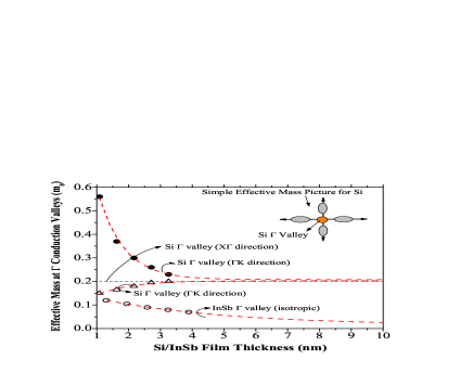
Fig. 10 shows the contour plot of the conduction and valence band energy dispersion for 8 atomic layers InSb thin film. We confirm that the valley in thin film still retains its isotropy unlike the case of Si low . Fig. 11 shows the Si and InSb thin film effective mass fitted from their 2D energy dispersion. InSb valley is isotropic with increasing effective mass as film thickness is scaled down. Si valley in thin film actually is originated from bulk valley, projected onto the 2D k-space. We observe that anisotropy in Si becomes more prominent with decreasing of film thickness, with the direction effective mass diverging for each of the two degenerate bands. The larger effective mass in Si is for the lower band of the two degenerate bands, and the smaller effective mass corresponds to the top band.
We have attempted to fit a parabolic dispersion to match the calculated energy dispersion to obtain the effective mass. In fact, we expect the effective mass to also increase with wave-vector as depicted in Fig. (7b). However, even if effective mass is not a rigorously derived quantity due to non-parabolic valleys, it serves as a very useful ’figure of merit’. Interestingly, the isotropic effective mass of InSb valley increases with the decrease of film thickness. At nm of InSb film, the effective mass is . Increase in would retard the quantization effect in InSb thin film. The isotropy of the electron mass, which translates to isotropy of the electron transport property, should be advantageous as it affords engineer with more flexibility in orientating the n and p-MOSFET devices to yield the most optimum transport direction on the same substrate.
IV Ballistic Limit of InSb Nanoscale Devices
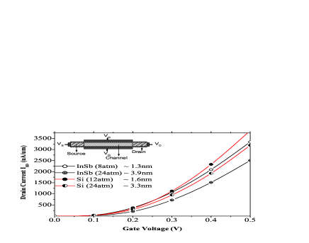
We calculated the InSb thin film devices’ ballistic current limit using the Non-Equilibrium Green’s Function (NEGF) method ren , under the framework of simple effective mass method. Since the energy dispersion for -surface InSb thin film is relatively isotropic (Fig. 10), one can employ a decoupled 2D treatment to the problem and calculation is done in the framework of mode-space NEGF approach ren . The effective masses used for the various InSb devices are as derived in Fig. 11. For Si devices, due to the anisotropy, we simply assumed an effective mass of . A double-gated device structure shown in Fig. 12 is employed. Channel length of 20 nm is used. An EOT of 1 nm and metal gate is employed. No wave function penetration into oxide is assumed. N-type Source/drain and p-type channel are doped at and respectively. The boundary conditions for the potential at the contact are set to floating, by imposing the condition that the potential derivatives are zero at these boundaries. The drive current vs. gate voltage is plotted in Fig. 12. The Si devices yield a slightly larger ballistic current compared to their InSb counterparts. The main reason is due to the larger density-of-states mass in Si and the fact that it is doubly degenerate compared to non-degenerate InSb valley. Currently, experimental study shows that sub 50 nm Si devices only achieve ballistic performance loc . A lower density-of-states mass should help damp the dissipative processes to achieve fully ballistic performances in InSb devices and performance then could be better than Si.
V Conclusion
Band structure of III-V material InSb thin films is calculated using empirical pseudopotential method (EPM). valley in InSb remains the lowest lying conduction valley (a desirable trait if high mobility characteristic is required) despite size quantization effects but its isotropic effective mass increases with decrease in the film thickness. A NEGF calculation of the InSb and Si double-gated devices reveals that they have comparable ballistic drive current.
Acknowledgments
This work is supported by Singapore A*STAR Nanoelectronics Program
under research grants R-398000019305. We gratefully acknowledge the
use of NanoMOS ren from Purdue
Computational Electronics Group for this work.
Appendix A treatment of spin-orbit coupling
The first starting point is the formulas in Ref. weisz , such as equation (A3) in it. To explicitly write down the formula of SOC, we shall calculate one of the terms of Eq. (A4) in Ref. weisz denoted as (II) here. We consider
| (5) | |||||
where and are quantum numbers characterizing the core states, , is the point located the unit cell, are the coordinates of atoms in the basis, , with being potential of atomic nuclei, is the angular momentum operator, is the Dirac function, is the volume of the unit cell, and is the number of unit cells in the crystal. By performing the integral over , and then let = and =. Then we have
| (6) | |||||
We denote the first square bracket in Eq. (6) by [A], the second one by [B] and the third square bracket by [C]. Each of these terms will now be individually analyzed. [A] includes the local position information of all atoms in a unit cell, as given by
| (7) |
where is the change in the wave vector. When we consider single-element crystal, there is only one kind of atom. If we set as the number of all atoms in a unit cell, then we have
| (8) | |||||
where
| (9) |
is the counterpart of the structure factor in Ref. weisz , and is the atomic volume in a unit cell so that .
The second square bracket [B] in Eq. (6) is
| (10) | |||||
where , are spherical harmonics and are spherical Bessel functions. We use the formula and are the spherical harmonic with the rotational index in any coordinate system with in the direction. Because of the orthogonality of spherical harmonics, the second square bracket in Eq. (10) gives , i.e., . Hence Eq. (10) simplifies to
| (11) |
where is the counterpart of B function defined in Ref. weisz , is the radial part of core wave function.
The third square bracket [C] in Eq. (6) as given by
| (12) | |||||
where angular part is
| (13) |
Here in spherical harmonics of angular part must be constrained by in Eq. (11). The same core states characterized by are expressed in the different coordinates. The term in Eq. (5) means the core states are projected into coordinates system in which direction is in . Similarly in , they are projected into (i.e. ) coordinates, in which direction is in . So we can write in Eq. (13) as . Then we get the angular part to be weisz
| (14) |
where are the associated Legendre polynomials, is the mutual angle between the vector and . From Eq. (14), (13) and (12), we get
| (15) |
where , which is similar to the ”A” function in Ref. (weisz ). Then we can get the term as
| (16) |
where the summations shall be taken over the quantum number and .
The other terms in (A3) in Ref. weisz can also derive from the similar calculations. Then the final expression of SOC can be written as
| (17) |
where and
| (18) |
where the first term comes from the plane wave (p)-core state (c), the second term comes from c-p, and the third comes from c-c term.
| (19) |
is about the spin orbit splitting of isolated atoms. It is just determined by local wave functions of core states. We shall discuss two cases.
Case one: two different atoms in a unit cell We set , and are corresponding to the two atoms. We get che
| (20) |
where are the symmetric (antisymmetric) contributions to the spin-orbit Hamiltonian.
Case two: multi-type and many atoms in a unit cell If we have species atoms in a unit cell, and , , , are numbers of atoms for each type atom in a unit cell. We have .
| (21) |
where is for -th species, and structure factor is , here summation over means over the atoms of -th species.
If we only keep the third term c-c in Eq. (18) (as in Refs. che ; walter ; bloom ) and only consider the main contribution from the outermost core state, i.e. orbit. Also note the relation , for , we have
| (22) |
where is selected as the quantum number characterizing the outermost core state, and is spin-orbit parameter for various atoms, we write it as . If we redefine the function by introducing a normalization constant as
| (23) |
where is determined by the limit . And in this procedure, an empirical adjustable parameter and describing the ratio of the spin-orbit contributions for free atoms and , see Refs. che . To evaluate the function explicitly, we may determine the expressions of the core state wave function and we use the formula in Ref. clementi
| (24) |
where are coefficients of expansion, and are Slater-type orbits with integer quantum numbers, namely
| (25) |
where
| (26) |
where and can be found in the tables in Ref. clementi . So the functions in Eq. (24) are
| (27) | |||||
In terms of these functions, we can calculate the integral as
| (28) | |||||
where and . The integral of can be easily derived when . It is
| (29) |
where . If we calculate the value of the limit , it shall be pointed out that the spherical Bessel functions can be formulated , where is a Bessel function of the first kind. Then we can get
| (30) |
This result is used to derive the normalization constant in Eq. (23).
References
- (1) ITRS 2004 (available on line) http://www.itrs.net/.
- (2) Bin Yu, Leland Chang, Shibly Ahmed, Haihong Wang, Scott Bell, Chih-Yuh Yang, Cyrus Tabery, Chau Ho, Qi Xiang, Tsu-Jae King, Jeffrey Bokor, Chenming Hu, Ming-Ren Lin, and David Kyser, 2002 IEDM Tech. Digest .
- (3) Komoda T, Oishi A, Sanuki T, Kasai K, Yoshimura H, Ohno K, Iwai M, Saito M, Matsuoka F, Nagashima N and Noguchi T, 2004 IEDM Tech. Digest 217.
- (4) Low T, Feng Y P, Li M F, Samudra G, Yeo Y C, Bai P, Chan L and Kwong D L, 2005 ISDRS (Semiconductor Device Research Symposium, 2005 International) p.384-p.385.
- (5) Fischetti M V, and Laux S, 1989 IEDM Tech. Digest pp.481-484.
- (6) Ashley T, Barnes A R, Buckle L, Datta S, Dean A B, Emeny M T, Hayes D G, Hilton K P, Jefferies R, Martin T, Nash K J, Phillips T J, Tang W H A, Wilding P J and Chau R, 2004 ICSICT (Solid-State and Integrated Circuits Technology, 2004. Proceedings. 7th International Conference on) 3, 2253.
- (7) Li M F, 1994 Modern Semiconductor Quantum Physics (Singapore: World Scientific).
- (8) Levinshtein M, Rumyantsev S, Shur M, 1996 Handbook series on semiconductor parameters (Singapore: World Scientific).
- (9) Pethe A, Krishnamohan T, Kim D, Saeroonter Oh, Wong H CS Philip, Nishi Y and Saraswat K C, 2005 IEDM p.605.
- (10) Harrison W A, 1966 Pseudopotentials in the theory of metals (Benjamin, Reading, Mass.).
- (11) Heine V, 1970 Solid State Physics, Vol. 24, eds. H. Ehrenreich, F. Seitz, and D. Turnbull (New York: Academic Press).
- (12) Zhu Z G, Low T, Li M F, Fan W J, Bai P, Kwong D L and Samudra G, 2006 IEDM Tech. Digest S31P2.
- (13) Fong C Y, and Cohen M L, 1970 Phys. Rev. Lett. 24, 306.
- (14) Cohen M L, and Bergstresser T K, 1966 Phys. Rev. 141, 789.
- (15) Cohen M L, Lin P J, Roessler D M and Walker W C, 1967 Phys. Rev. 155, 992.
- (16) Wang L W, and Zunger A, 1994 J. Phys. Chem. 98, 2158.
- (17) Wang L W, and Zunger A, 1994 J. Phys. Chem. 100, 2394.
- (18) Xia Jian-Bai, and Cheah K W, 1997 Phys. Rev. B 55, 15688.
- (19) Yeh Chin-Yu, Zhang S B, and Zunger A, 1994 Phys. Rev. B 50, 14405.
- (20) Xia Jian-Bai, and Cheah K W, 1997 Phys. Rev. B 56, 14925.
- (21) Zhang S B, Yeh Chin-Yu, and Zunger A, 1993 Phys. Rev. B 48, 11204.
- (22) Van de Walle C G, Martin R M., 1987 Phys. Rev. B 35, 8154; 1989 Phys. Rev. B 39, 1871.
- (23) Segall M D, Lindan P J D, Probert M J, Pickard C J, Hasnip P J, Clark S J and Payne M C, 2002 J. Phys.: Cond. Matt. 14, 2717.
- (24) Raghavachari K, Fu Q, Chen G, Li L, Li C H, Law D C, and Hicks R F, 2002 J. AM. Chem. SOC. 124, 15119.
- (25) Balázs G, Breunig H J, Lork E, and Offermann W, 2001 Organometallics 20, 2666.
- (26) Weisz G, 1966 Phys. Rev. 149, 504.
- (27) Chelikowsky J R, and Cohen M L, 1976 Phys. Rev. B 14, 556; 1984 Phys. Rev. B 30, 4828.
- (28) Walter J P, Cohen M L, Petroff Y, and Balkanski M, 1970 Phys. Rev. B 1, 2661.
- (29) Bloom S, and Bergstresser T K, 1970 Phys. Stat. Sol. 42, 191.
- (30) Ren Z, Venugopal R, Goasguen S, Datta S, and Lundstrom Mark S, 2003 IEEE Transactions on Electron Devices, 50, 1914.
- (31) Lochtefeld A, and Antoniadis D A, 2001 IEEE Electron Device Letters, 22, 95.
- (32) Clementi E, and Roetti C, 1974 Atomic Data and Nuclear Data Tables, 14, 177-478.