Topological Anderson insulator phenomena
Abstract
We study the nature of the disorder-induced quantized conductance, i.e., the phenomena of topological Anderson insulator (TAI) induced in HgTe/CdTe semiconductor quantum well. The disorder effect in several different systems where anomalous Hall effect exist, is numerically studied using the tight-binding Hamiltonian. It is found that the TAI phenomena also occur in the modified Dirac model where the quadratic corrections is included and electron-hole symmetry is kept. It also occurs in the graphene system with the next nearest-neighbor coupling and staggered sublattice potential. Comparison between the localization lengths of the 2D ribbon and 2D cylinder clearly reveals the topological nature of this phenomena. Furthermore, analysis on the local current density in anomalous quantum Hall systems where the TAI phenomena can or can not arise reveals the nature of TAI phenomena: the bulk state is killed drastically and only the robust edge state survives in a moderate disorder. When the edge state is robust enough to resist the strong disorder that can completely kills the bulk state, TAI phenomena arise.
pacs:
73.23.-b, 73.43.-f, 73.20.At, 72.15.Rn,I introduction
It is known that the two-dimensional (2D) noninteracting system with the quadratic dispersion relation is an Anderson insulator.TAI
XXX
In the presence of strong spin orbit coupling (SOC)soi ; Qiao , the externalQiao ; ShengDN or internalHaldane magnetic field, the metallic state is present. Due to the crossing of the mobility edgeOnoda , a metal-insulator transition (MIT) occurs at the critical disorder strength where the localization is divergent. Recently, Li et alLiJian find that the disorder drive either a metallic state or an ordinary insulating state to the topological insulator (it is so called topological Anderson insulator) in the HgTe/CdTe quantum well, which has been numerically confirmed by Jiang et elJiangHua . Using the effective medium theory, the mechanism of the TAI is explained as the crossing of a band edge rather than a mobility edge by Groth et al.Beenakker Although there are many investigations focused on the TAI, there are still some unanswered questions. For instance, what leads to the band edge crossing, or, what’s the nature of the TAI phenomena (i.e., disorder induce quantized conductance)? Furthermore, except for HgTe/CdTe quantum well, is there any other systems that have TAI phenomena? What’s the necessary condition to generate TAI phenomena?
As we know, the edge states in topological insulatortopoInsulator are “helical” states, i.e., the direction of propagation is tied to the electron spin rather than electron charge, the edge states located in the opposite edges are protected by the time reversal symmetry and each contribute to the conductance. In principle, we can focus only on one edge state which is tied to spin up or spin down to study topological insulator. The sub-system related to each individual spin contribute to an individual anomalous quantum Hall effect. In the following, we will deal with the sub-system related to the spin up in topological insulator and treat it as an individual anomalous quantum Hall effect.
In a 2D anomalous quantum HallQiao1 ; QAH system, the topological edge states connect the energetically separated continuum of energy band, and only the unidirectional topological edge state contribute to the conductance in the band gap. Due to the topological stability of Chern numbersChernNum carried by the extended states, the conductance remains quantized in the presence of weak disorder. At strong disorders, the mobility edges is crossed, and MITOnoda ; ShengDN occurs. However, outside of the gap, the bulk state and edge state may co-exist. Because the edge state is robust for disorders, it could happen that the bulk state is completely killed before the edge state is killed, which may lead to the quantized conductance plateau. The quantized value is determined by the number of the robust edge state. Taking into account of edge state tied to both the spin up and spin down, disorder induced TAI can be formed, which is confirmed by the following calculation on the modified Dirac model. So, roughly speaking, as long as the bulk states and the robust enough edge state coexist in the system, disorder induced quantized conductance can emerge.
In this paper, in order to effectively study the nature of TAI phenomena, in addition to HgTe/CdTe quantum well,ZhangSC we first find two other different models in which TAI phenomena also exists as in Ref.LiJian, . The first model is a modified Dirac model on a square lattice with the quadratic corrections included and electron-hole symmetry kept. This model is similar to HgTe/CdTe quantum well model except the e-h symmetry is broken in HgTe/CdTe quantum well.ZhangSC The second model is a graphene model on a honeycomb lattice with the next nearest-neighbor coupling and a staggered sublattice potentialHaldane . In this model the e-h symmetry and inversion symmetry are all broken, and the anti-directional topological edge states tied to two opposite edges are asymmetrically distributed. Our calculation shows that in the first and second models, moderate disorder induces a transition from an ordinary metallic state to a TAI with the quantized conductance of . The wider the ribbon is, the smaller the fluctuation. In the disorder induced quantized conductance regime, the localization length of the ribbon structure is extremely long comparing to that of the cylinder structure, which clearly reveals the topological origin of the transition. When the disorder is very strong, mobility edge crosses and MIT occurs. This process is related to the bulk state. In order to vividly show how the transport electron is scattered by the disorder, we calculate the individual local current density from all channels including the edge state channel and bulk state channel. In addition to the first and second model, we also calculate local current density in a third model: the honeycomb graphene systemQiao1 in which we consider Rashba spin-orbit interaction, exchange energy and staggered sublattice potential. In the third model, the disorder can’t quantize the conductance but just flatten it, which is different from the first and second model. However, for all three models, we find that disorder kill all the bulk current and induce edge current with uni-direction. It means that in the process of transport, due to the topological nature, the edge state is maintained all the time, no matter whether it is kept in the edge channel or scattered into the bulk channels. So, in the system where the edge state and bulk state coexist, in the moderate disorder, the edge state is maintained while the bulk states are killed, which leads to the flattened conductance. If the edge state is robust enough to resist the disorder that is so strong that the bulk state are completely killed, quantized conductance can be formed.
The rest of the paper is organized as follows. In Sec. II, the Hamiltonian of three model systems in the tight-binding representation are introduced. The formalisms for calculating the conductance and the local current density vector are then derived. Sec. III gives numerical results along with some discussions. Finally, a brief summary is presented in Sec. IV.
II models and formalism
II.1 three model Hamiltonian
The first model is the modified Dirac model with a quadratic corrections , which has the form
| (1) |
where are Pauli matrices presenting the pseudospin formed by orbitals, In Eq.(1), the momentum is a good quantum number for periodic systems. This model is similar to the low-energy effective Hamiltonian of a HgTe/CrTe quantum wellZhangSC except that the e-h symmetry is kept here while it is broken in HgTe/CrTe quantum well. Using substitution and Eq.(1) can be transformed into the real space representation.book In the calculation we consider the infinite long ribbon with finite width, hence the tight-binding representation is convenient. The tight-binding Hamiltonian in square lattice is given by:LiJian ; JiangHua
| (2) | |||||
where is a unitary matrix, is a random on-site potential which is uniformly distributed in the region . is the index of the discrete site of the system sketched in the Fig.1(a) on the square lattice, and are the unit vectors of the square lattice with the lattice constant . with denoting transpose and and are the annihilation and creation operators for s(p) orbital at site . Here and denote the nearest neighbor coupling strength. in the first term of Eq.(2) is the on-site random energy account for the disorder. The second term in Eq.(2) is the corrected linear Dirac term, in which the involved terms are the quadratic corrections to the Dirac Hamiltonian. The individual spin up Hamiltonian and spin down Hamiltonian in Eq.(2) are time reversal symmetric to each other. Since they are decoupled, we can deal with them individually. So we shall focus only on spin-up Hamiltonian in the following calculation.
The second model is proposed by Haldane that considers the graphene with next-nearest neighbor coupling and staggered sublattice potential whose Hamiltonian can be expressed as:Haldane
| (3) |
where are Pauli matrix denoting the pseudospin formed by AB sublattice, three nearest neighbor unit vectors and next-nearest neighbor unit vectors are given by , , , , , with and denoting the distance between nearest neighbor sites (lattice constant) and next-nearest neighbor sites respectively. In Eq.(3), is the staggered sublattice potential, is the nearest neighbor coupling strength with Fermi velocity , the next-nearest neighbor coupling where and are the coupling strength and phase deduced from the effective internal magnetic field along direction. Here eliminates the e-h symmetry of the energy bands as shown in Fig.2(b) and breaks the time-reversal invariance. Eq.(3) is similar to Eq.(1), which includes all the terms that is -dependent. However, they have different symmetries, e.g., in Eq.(3) both time-reversal and e-h symmetries are broken. In the tight-binding representation, Eq.(3) can be expressed as:
| (4) | |||||
where is the index of the discrete site of the honeycomb lattice which includes two sublattice A (open circle) and B (filled circle) as sketched in the Fig.1(b). ) denotes the random potential induced by disorder, , and are the annihilation and creation operators for sublattice A(B) at site .
In the third model, we consider a graphene sheet with Rashba spin-orbit interaction as well as an exchange field.Qiao1 In the tight-binding representation on the honeycomb lattice, corresponding to three directions of translational symmetry, we have . Projecting them to the and direction, we can get and . Then, the Hamiltonian of the third graphene model including Rashba spin-orbit coupling, the staggered sublattice potential and the exchange term can be expressed in the tight-binding representation in the following form:ShengL
| (5) | |||||
where is the unitary matrix in spin space, , are Pauli matrix denoting the real spin, , , where and are the creation operators for sublattice A and B for spin up(down) at site . ) is the random potential induced by disorder. Similar to the Hamiltonian of the second model, is the nearest neighbor coupling and describes the staggered sublattice potential. In Eq.(5), is the exchange energy which can be achieved by either a magnetic insulator substrate or adsorbing transition metal atoms (e.g., iron, copper) on graphene.Qiao1 Finally is the strength of Rashba spin-orbit coupling that has been shown to be fairly strong.Rashba
II.2 differential current density and conductance
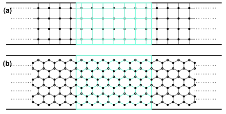
In the following, we consider two geometries: ribbon and cylinder. Fig.1(a) and (b), respectively, depict the ribbon geometry on square lattice and honeycomb lattice. In these systems the finite scattering region [green (or gray in print) region], in which random disorder is considered, is connected to the external reservoir through semi-infinite lead. In the following, we will derive the conductance and the current density in the scattering region.
For the general Hamiltonian , local current flowing from site with real spin or pseudospin can be expressed as:Jauho
| (6) | |||||
where is the electron charge, is the matrix element of the lesser Green’s function of the scattering region. Here is the current from site i to j. Under dc bias, the current is time-independent. After taking Fourier transform, current can be written as:
| (7) |
Due to the current conservation, at each site inside the scattering region. From now on, we will calculate the current density from . For the square lattice, it is easy to calculate the current density by summing over all projections of along x and y directions as done in Ref.JiangHua, ; lens, ; LiJian1, . However, it is much more complicated for graphene because in the tight-binding representation on graphene, the current can flow from site i to its nearest and next nearest neighbor sites j. Hence we will use another simple definitionCurrentDensity of current density where is the charge density and is the velocity given by . The current density is
| (8) |
where is a diagonal matrix in the discrete real space. It should be noted that Eq.(8) is valid when site i is not on the interface between the lead and the scattering region. For these boundary sites, the current density perpendicular to the interface obtained from Eq.(8) should be multiplied by two. This is due to the following reason. When we have a finite scattering, the current is conserved if the self-energy is taken into account. However, for these boundary sites the current from the lead is not accounted for by Eq.(8).
From the Keldysh equation, the lesser Green’s function is related to the retarded and advanced Green’s functions,
| (9) |
where the sum index denote the left and right semi-infinite lead, in Eq.(9) is the lesser self energy of the lead- with the Fermi distribution function. Here and is related to the surface Green’s function which can be calculated using a transfer matrix method.transfer is the external bias in the terminal-. In general, can be divided into equilibrium and non-equilibrium parts,lens
| (10) | |||||
where the equilibrium term can only generate persistent currentfoot and does not contribute to the transport,persistent so it can be dropped out from now on. It is the non-equilibrium term that gives the response to the electron injection from the source lead. Setting source bias and drain bias , we have
| (11) |
where is the linewidth function of source lead. Substituting Eq.(11) into Eq.(8), the differential local current density vector at site can be expressed in the following form:foot1
| (12) |
with
| (13) | |||
where and are density matrix with incident energy and velocity matrix in the central scattering region, respectively and we have assumed the temperature is zero.
XXX
When the electron is in the eigenmodes of the semi-infinite lead there is no scattering, the the linewidth function of source lead is related to the incident velocity in the form XiaKe where is diagonal matrix composed by the nonzero velocity in propagating mode and zero velocity in evanescent mode, is ranked by eigenmodes including propagating mode and evanescent mode, here can be considered as a unitary transformation matrix which transforms the general Hilbert space into the eigen channel space of lead. Then, can be regarded as incoming velocity matrix in source lead with relation [for detail please refer to Ref.XiaKe, ]. In the calculation, we can peak up only the propagating mode to construct the effective linewidth function as
| (14) |
where the sum is taken over propagating modes. is the -th column of matrix which is related to the -th propagating mode. Then from Eq.(12),(13), we can write the differential local current density vector in -th propagating eigenchannel:
| (15) |
where
| (16) |
Concerning for the scalar current flowing into the drain lead and the conductance , we can replace with in Eq.(12) where is the effective outgoing velocity matrix of drain lead similar as effective incident velocity matrix in source lead. Then, considering the representation transformation, from Eq.(12), (13), we can get the Landauer-Buttikker formulaLanduaer , which leads to conductance in zero temprature
| (17) |
where is the transmission coefficient from source lead to drain lead.
III numerical results and discussion
In the numerical calculations, the energy is measured in the unit of the nearest neighbor coupling constant . For the first model, with the square lattice constant . For the second and third model in the honeycomb lattice, with the carbon-carbon distance and the Fermi velocity as in a real graphene sample.ref3 The size of the scattering region [the green (or gray in print) region] is described by integers and corresponding to the width and length, respectively. For example, in Fig.1, the width with , the length with in the panel (a), and the width with , the length with in the panel (b).
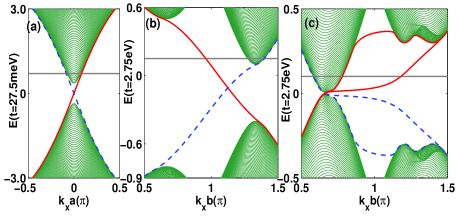
In all three models Eq.(2), (4) and (5), edge state exists in the absence of external magnetic field, which induce the quantum anomalous Hall effect. In Fig.2, we plot the band structure (for calculation see Ref.band, ) and indicate the Fermi energy (the gray lines) in three models. We can see the unidirectional edge states along the each edge, down edge [the state in the blue (or dark gray in print) dashed lines] or up edge [the state in the red (or light gray in print) lines] in these models. For the first model [panel(a)], since e-h symmetry is kept so that we can focus only on electrons, i.e., only the positive energy is considered. This is different from the HgTe/CdTe quantum well, in which e-h symmetry is broken and the edge state is more localized along the edge for the positive energy than the negative energy. In the calculation we set Fermi energy , , , , . For the second model [panel (b)], the following parameters are used: Fermi energy , the nearest neighbor coupling constant that is used as the energy unit in the graphene models, the next-nearest neighbor coupling strength , the staggered sublattice potential . In this model, e-h symmetry is broken by the next-nearest neighbor coupling , and the edge states are favored the hole system (negative energy). In the third model, different from the second one, the next-nearest neighbor coupling is absent, the Rashba SOC and exchange energy are considered, Fermi energy . Due to the Rashba SOC, the spin degeneracy is lifted and there are two unidirectional edge states [red or blue lines in panel (c)] corresponding to different spins. In the second and third models, we find that the staggered sublattice potential is important to study the nature of TAI phenomena. First, breaks the inversion symmetry, the left [red line in Fig.2(b), blue line in Fig.2(c)] and right flowing edge states as well as the bulk states are asymmetrically distributed as shown in Fig.2(b) and (c). As a result, the left and right injected current density are distributed differently, although they contribute to the same total current. Second, makes the bulk gap smaller, which leads to the coexistence of the robust edge state and bulk states in certain energy window . For instance in Fig.2(b) where only one edge state near the upper edge that coexist with the bulk states. In Fig.2(c), the bulk gap is closed completely, as will be discussed later that for this case it is harder to induce the TAI phenomena. However this model can give us some insight about TAI phenomena.
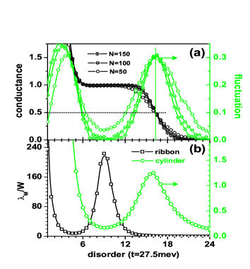
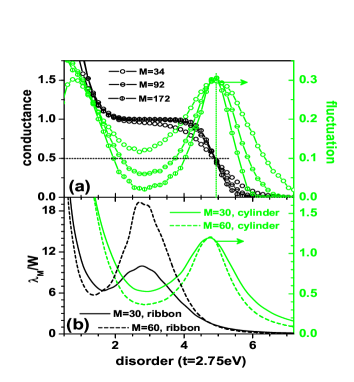
In Fig.3(a) and Fig.4(a), we plot conductance and its fluctuation vs disorder for the first model in a square lattice and the second model in a honeycomb lattice, respectively. In Fig.3(a), Fig.4(a) and Fig.5, all data are obtained by averaging over 5000 configurations. In Fig.3(b) and Fig.4(b), we also plot the renormalized localization length of a 2D strip with the width for the square lattice [Fig.3(b)] and for the honeycomb lattice [Fig.4(b)]. Furthermore, in order to highlight the topological nature, we also plot the renormalized localization length in a 2D cylinder sample (where the edge state is removed) with diameter . Here the Fermi energy is set in the bulk state [see Fig.2]. In the clean system with , the conductance is contributed by bulk states and one edge state. When disorder is introduced, the following observations are in order: (1) the small disorder rapidly suppresses the conductance and enhances its fluctuation. This means that the system is leading to the diffusive regime, in which the bulk extended state is scattered by impurities and gradually becomes localized by disorder. As a result, the localization length decreases accordingly for both strip and cylinder samples. (2) at moderate disorders, in the strip sample, the conductance stops decreasing and develops into a quantized plateau, a new phase occurs. At the same time, the fluctuation is deduced to almost zero, indicating the formation of either a bulk insulator or metallic phase. The abruptly increased localization length (black lines) in panel (b) clearly indicates the metallic phase induced by edge state. For the cylinder sample, however, because of the absence of the edge state, the system can only develop into the bulk insulator, so the localization length continues to decrease. Our results show that the wider the ribbon is, the larger in ribbon geometry and the smaller in cylinder geometry [see Fig.4(b)]. Therefore, concerning , the peak structure in strip geometry and the valley structure in cylinder geometry clearly indicate the topological nature of the TAI phenomena. (3) when the disorder is strong, the quantized conductance plateau in the strip sample starts to deteriorate and its fluctuation begins to increase. This shows that the edge state will be destroyed at the strong disorder and the system will enter the insulating regime.
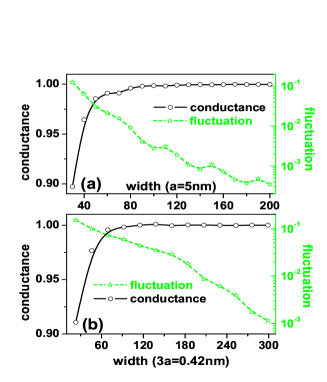
For the cylinder sample, there is only one system transforms from band insulator to Anderson insulator. The peak of indicates the transition points. (4) at the critical disorder strength MIT occurs. is marked in Fig.(3) and (4) by the vertical green gray in print) dotted lines, where conductance and . For cylinder sample, diverges at . It should be noted that despite of the different topological nature, the MIT occurs at nearly the same for strip and cylinder samples. (5) in the quantized conductance regime, increasing the sample size, the quantized plateau is much wider with smaller fluctuation. This is not surprising since for the larger sample, the bulk state is scattered more frequently while the overlap of opposite unidirectional edge states is smaller. This size effect is clearly seen in Fig.5, in which the quantized conductance and its fluctuation in the midpoint [ for panel (a) and for panel(b)] of conductance plateaus are plotted vs width of square sample for the fist model and second models. We can see with the increasing of the sample size, the conductance eventually saturates to the quantized value, its fluctuation, however, continues to drop. It is expected that when the size is large enough, the complete quantized plateau will be formed with no conductance fluctuation.
Up to now, we have confirmed that in addition to the HgTe/CdTe quantum well, the TAI, i.e., disorder induce quantized conductance can also occur in other systems such as the Dirac model and the graphene system. XXX Since the phenomenon of TAI is not the particular properties of HgTe/CdTe quantum well, there must be the common nature of TAI phenomena in different systems. For this reason, we study the scattering process in different systems through monitoring the local current density.
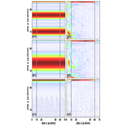
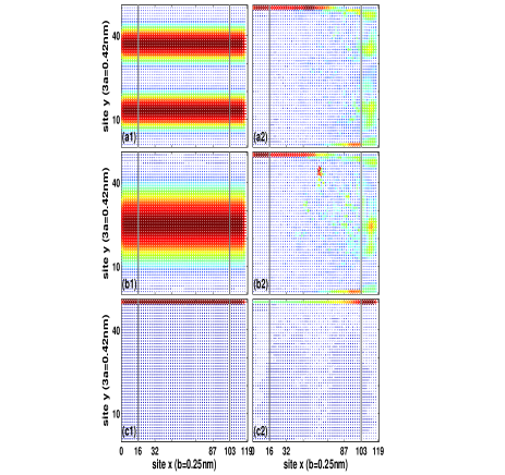
First we study the Dirac model. Due to the inversion symmetry in the Dirac model, the left and right injected current are equivalent, here we focus only on the left injected current. We have set Fermi energy to be for Fig.6. In Fig.6, Fig.8, Fig.8, and Fig.10, all data are obtained by averaging over 1000 configurations. For , there are several transmission channels and we have studied the first three transmission channels, one is edge state and the other two are bulk states. In Fig.6(a)-(c), we plot the left injected local differential current density distribution from the lowest three transmission-channel including the edge channel [panel (c)] and the first [panel (b)] and second [panel (a)] bulk channel in a square sample [between two vertical gray lines]. For the clean system with [the left column], the system is ballistic and there is no scattering. So, the current density from all transmission channels are distributed along the transport direction. For the left column of Fig.6, we can see the right going edge state on the upper edge and the extended bulk state with one or two transverse peaks in the current density. Note that the coming eigen-channels are classified according to the lead. When disorder is present, due to the mode mixing the electron in edge channel can be scattered into bulk channels and vice versa. As a result, the eigen-channels of the lead are no longer the eigen-channels of the system. Corresponding to the left column of Fig.6, in right column, we plot the current density distribution at the entrance of the TAI (quantized conductance) with . We can see that the right going edge current in all transmission-channels of the lead are well protected.
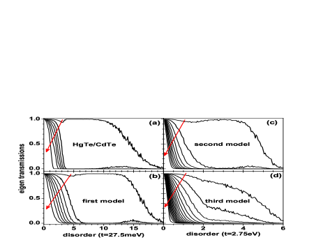
In order to study the nature of the edge state in the presence of disorders, we have calculated the eigen-spectrum of the transmission matrix .Qiao_new In Fig.7(b), we plot all the transmissions of eigen channels for the the first and second model. For comparing, in Fig.7(a), we also plot the eigen transmissions of HgTe/CdTe quantum well in which except for the terms in the first model, the term of are also included. Here, we set with and the other parameters are same as in the first model. In Fig.7, all data are obtained by averaging over 100 configurations. We found that there is always one eigen-value that is nearly equal to one which is identified as edge state by examining its current density profile. It illuminate that due to the topological nature, the edge state is always protected during the transport, although it may be scattering into the bulk channels of lead.
From Fig.7, we also found that the eigen transmissions of the first and second model in this paper exhibit the same properties as that in the HgTe/CdTe quantum well. It strongly implies they have the same
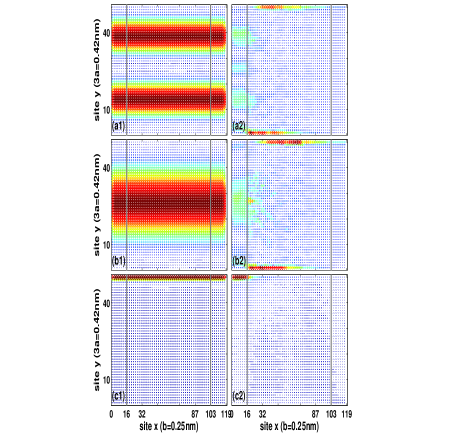
Next, we examine the graphene model. We set for Fig.8 and Fig.9. In the graphene model, the staggered sublattice potential is considered, which breaks the inversion symmetry, and the configuration of left and right injected current density are different. In a clean system, the left (right) injected current is contributed by the states that have a positive (negative) group velocity, i.e., . For the fixed Fermi energy, the crossing of Fermi energy and energy band determines the momentum of all propagating states. From the band structure of the graphene model [Fig.2(b) and (c)], we can see that the edge state is absent for the right propagating band in the second model while in the third model, it is absent for the left propagating state.
In Fig.8 and Fig.9, we plot the left and right injected current density in the second model, respectively. We can see that for the left injected current, although edge current is absent in clean limit, it emerges when disorder is turned on. This can be understood as follows.Beenakker When the disorder is present, the effective medium theory similar to the one in Ref.Beenakker, shows that the parameters in the second model such as and are all renormalized and depend on disorder strength. After renormalization due to the disorder, the new Fermi level (renormalized) is inside the bulk gap of the new band structure giving rise to a true edge state.
Besides, the random disorder also eliminates the difference between states with different momentum due to its random distribution. So, although the profiles of left and right injected current density are different in the clean system, when the moderate disorder is considered they tend to be the same since the bulk state are killed and only edge state survives [see Fig.7 and Fig.8]. Of course, the left going and right going edge states are along the opposite edge. Similar to the first model, in clean limit, the current density in all eigenchannels are kept and uniformly distributed along the transport direction, except they have different profiles for left and right injected current density.
XXX
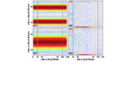
Form Fig.6, 8 and 9, it seems that the phenomena of disorder induce quantized conductance can appears in any system where quantum anomalous Hall effect is hold. However, it shoulder be noted that in the first and second model, the edge state is robust so that they can penetrate into the scattering region under the interface scattering. In this way, the quantized is formed. In the following we will study another quantum anomalous Hall system, it is the third model. Similar to the second model, due to the inversion asymmetry, the configuration of the left and right injected current density are different in the clean limit, here we focus only on the left injected case in which the edge current is present in clean system. In the third model, the bulk energy gap is closed by the staggered sublattice potential, there is no pure edge state for any incident energy, so the edge state is not so robust as in the first and second model. Furthermore, due to inversion asymmetry, one of the two unidirectional edge states turns into bulk state [see Fig.2(c)]. So the disorder induced conductance must be if any.
As a result, because the edge state is not so robust, the back following edge current is strong, although there is one unambiguous unidirectional edge state [see left column of Fig.10], it is drastically reflected by the interface scattering, then the edge current can’t deeply penetrate into the scattering region when moderate disorder strength is considered, which can be clearly seen in Fig.10(c2). On the other hand, the edge state that enter into the scattering region can always survive in a moderate disorder [see Fig.10(a2) and (b2)]. As a result, the conductance can’t be quantized but flattened by the moderate disorder, which is different from the first and second model, but they share the same nature, that can also be seen from Fig.7(c) and (d).
In Fig.7(c) and (d) we plot the system eigen transmissions of the second and third model. We can see for all model (the first, second, third model and the HgTe/CdTe quantum well), the transmissions of eigen bulk state are rapidly reduced to zero in a weak disorder, while the eigen edge state can be kept in the moderate disorder. When the eigen edge state is robust, it can be completely kept [transmission equal to one, see panel (a), (b) and (c)], but when the eigen edge state is not so robust, it can only be partly kept [transmission is smaller than one, see panel (d)]. So we can conclude that in the system where robust edge state and bulk state coexist, the edge state is maintained while the bulk states are killed in the moderate disorder, which leads to the flat conductance. If the edge state is robust enough to resist the disorder that is so strong that the bulk state are completely killed, quantized conductance can be formed and TAI phenomena appears.
IV conclusion
In summary, the disorder effect is studied in several quantum anomalous Hall system. When beyond the energy gap, the edge state and bulk state often coexist in clean system or weak disorder system. In a moderate disorder, the inter-band scattering happens. If the edge state is robust enough to resist the interface scattering, it can penetrate deep into scattering region where the edge state and bulk state coexist in all of the coming eigen channels due to the mod mixing. Due to the topological nature, the bulk states are drastically killed and edge state survives. In the eigen spectrum of the whole system, the eigen channel corresponding to the edge state is kept well and the other bulk channels are completely killed, which leads to a flattened conductance accompanied with the rapidly decreased fluctuation. In several spatial systems such as HgTe/CdTe quantum well, modified Dirac model and the graphene system with next-nearest coupling and staggered sublattice potential, the edge state is very robust so that it can survive in a disorder that is so strong that the bulk states are completely killed by them. Without the bulk states, the unidirectional edge state located in up or down edge can’t be transformed to the opposite edge, the the back following current is then prohibited. As a result, the quantized conductance can be formed and TAI phenomena that disorder induce quantized conductance appears.
We gratefully acknowledge the financial support by a RGC grant (HKU 705409P) from the Government of HKSAR.
References
- (1) Electronic address: jianwang@hkusua.hku.hk
- (2) E. Abrahams, P. W. Anderson, D. C. Licciardello, and T. V. Ramakrishnan, Phys. Rev. Lett. 42, 673 (1979).
- (3) S. Murakami, N. Nagaosa, and S. C. Zhang, Science 301, 1348 (2003); Phys. Rev. B 69, 235206 (2004); J. Sinova, D. Culcer, Q. Niu, N. A. Sinitsyn, T. Jungwirth, and A. H. MacDonald, Phys. Rev. Lett. 92, 126603 (2004); L. Sheng, D. N. Sheng and C. S. Ting, Phys. Rev. Lett. 94, 016602 (2005).
- (4) Z. Qiao, Y. Xing, and J. Wang, Phys. Rev. B 81, 085114 (20010).
- (5) D. N. Sheng and Z. Y. Weng, Phys. Rev. Lett. 80, 580 (1998).
- (6) F. D. M. Haldane, Phys. Rev. Lett. 61, 2015 (1988).
- (7) M. Onoda and N. Nagaosa, Phys. Rev. Lett. 90, 206601 (2003); M. Onoda, Y. Avishai, and N. Nagaosa, Phys. Rev. Lett. 98, 076802 (2007); H. Obuse, A. Furusaki, S. Ryu, and C. Mudry, Phys. Rev. B 76, 075301 (2007).
- (8) J. Li, R.L. Chu, J. K. Jain and S.Q. Shen, Phys. Rev. Lett. 102, 136806 (2009).
- (9) H. Jiang, L. Wang, Q.-F. Sun and X. C. Xie, Phys. Rev. B 80, 165316 (2009).
- (10) C. W. Groth, M. Wimmer,1 A. R. Akhmerov, J. Tworzydło and C. W. J. Beenakker, Phys. Rev. Lett. 103, 196805 (2009).
- (11) C.-X. Liu, X.-L. Qi, H. Zhang, X. Dai, Z. Fang, and S.-C. Zhang, Phys. Rev. B, 82, 045122 (2010); S. Raghu, X.-L. Qi, C. Honerkamp, and S.-C. Zhang, Phys. Rev. Lett., 100, 156401 (2008); B. A. Bernevig and S.-C. Zhang, Phys. Rev. Lett. 96, 106802 (2006); C. L. Kane and E. J. Mele, Phys. Rev. Lett. 95, 22801 (2006).
- (12) Z. Qiao, S. A. Yang, W. Feng, W.-K. Tse, J. Ding, Y. Yao, J. Wang, and Q. Niu, Phys. Rev. B, 82, 161414 (2010).
- (13) R. Nandkishore and L. Levitov, Phys. Rev. B 82, 115124 (2010); Y.-F. Hsu and G.-Y. Guo, Phys. Rev. B 82, 165404 (2010).
- (14) D. N. Sheng, Z. Y. Weng, L. Sheng and F. D. M. Haldane, Phys. Rev. Lett. 97, 036808 (2006); D. Xiao, M.C. Chang and Q. Niu, Rev. Mod. Phys. 80, 1355 (2008).
- (15) B. A. Bernevig, T. L. Hughes, and S.-C. Zhang, Science 314, 1757 (2006); C.-X. Liu, X.-L. Qi, X. Dai, Z. Fang, and S.-C. Zhang, Phys. Rev. Lett. 101, 146802 (2008).
- (16) Electronic Transport in Mesoscopic Systems, edited by S. Datta (Cambridge University Press, 1995).
- (17) L. Sheng, D. N. Sheng, C. S. Ting,1 and F. D. M. Haldane, Phys. Rev. Lett. 95, 136602 (2005).
- (18) Y. S. Dedkov et al., Phys. Rev. Lett. 100, 107602 (2008).
- (19) A.-P. Jauho, N. S. Wingreen, and Y. Meir, Phys. Rev. B 50, 5528 (1994).
- (20) Y. Xing, J. Wang and Q.-F. Sun, Phys. Rev. B 81, 165425 (2010).
- (21) J. Li and S.-Q. Shen, Phys. Rev. B 76, 153302 (2007).
- (22) B. K. Nikolić L. P. Zârbo and S. Souma, Phys. Rev. B 73, 075303 (2006).
- (23) D. H. Lee and J. D. Joannopoulos, Phys. Rev. B 23, 4997 (1981); ibid, 23, 4988 (1981).
- (24) Here the persistent current is due to the magnetic vector potential . If , equilibrium current is zero because the left and right lead contribute opposite current density considering the symmetry properties.CurrentDensity
- (25) A. Cresti, G. Grosso, and G. P. Parravicini, Phys. Rev. B 69, 233313 (2004).
- (26) The expression should be modified when the site is on the boundary of the scattering region.
- (27) P. A. Khomyakov, G. Brocks, V. Karpan, M. Zwierzycki, and P. J. Kelly, Phys. Rev. B 72, 035450 (2005).
- (28) T. P. Pareek, Phys. Rev. Lett. 92, 076601 (2004); Y. Xing, Q.-F Sun, and J. Wang, Phys. Rev. B, 73, 205339 (2006); ibid, 80, 235411 (2009).
- (29) K. Novoselov et al., Nature 438, 197 (2005); Y. Zhang, Y.-W. Tan, H. L. Stormer, P. Kim, Nature 438, 201 (2005); K. Novoselov et al., Nature Phys. 2, 177 (2006); J. R. Williams, L. Dicarlo and C. M. Marcus, Science 317, 638 (2008).
- (30) Y. Hatsugai, Phys. Rev. B 48, 11851 (1993).
- (31) Z. Qiao, J. Wang, Q.-f. Sun and H. Guo, Phys. Rev. B 79, 205308 (2009).