Current oscillations in Vanadium Dioxide:
evidence for electrically triggered percolation avalanches
Abstract
In this work, we experimentally and theoretically explore voltage controlled oscillations occurring in micro-beams of vanadium dioxide. These oscillations are a result of the reversible insulator to metal phase transition in vanadium dioxide. Examining the structure of the observed oscillations in detail, we propose a modified percolative-avalanche model which allows for voltage-triggering. This model captures the periodicity and waveshape of the oscillations as well as several other key features. Importantly, our modeling shows that while temperature plays a critical role in the vanadium dioxide phase transition, electrically induced heating cannot act as the primary instigator of the oscillations in this configuration. This realization leads us to identify electric field as the most likely candidate for driving the phase transition.
I Introduction
Vanadium Dioxide (VO2) has been a material of prolonged scientific interest, due to the plethora of unusual properties associated with the Insulator to Metal phase Transition (IMT) occurring just above room temperatureMorin (1959). The large conductivity change ratio, combined with an accessible transition temperature and rich correlated-electron physics Qazilbash et al. (2007, 2008a); Liu et al. (2009) has made this an attractive compound for many researchers. Much attention has historically revolved around controversy over the driving physics of the phase transition; particularly whether it is a Mott transition Zylbersztejn and Mott (1975); Kim et al. (2004); Rice et al. (1994) or Pierels transition Qazilbash et al. (2007); Wentzcovitch et al. (1994); Cavalleri et al. (2004). However, also of interest is the ability of the IMT to happen on ultrafast (100fs) timescalesCavalleri et al. (2001), and the wide range of stimuli which can trigger itRini et al. (2005); Lysenko et al. (2006). Along these lines, recent interest has also shifted from purely academic to industrial as well; following proposed applications ranging from optical devices Lopez et al. (2004) and hybrid-metamaterials Driscoll et al. (2008, 2009a); Dicken et al. (2009) to electronic components Kim et al. (2006); Driscoll et al. (2010) and data storage Driscoll et al. (2009b); Pershin (2011). With this rise of potential applications comes opportunities for new avenues of research and development, but also new challenges to satisfy the durability and flexibility that real-world devices demand Crunteanu et al. (2010). Understanding the role of temperature and structural transitions in various VO2 phenomenon is key to pushing towards potential of applications.
In this manuscript we take an interest in the recently reported Lee et al. (2008); Sakai (2008) phenomenon of self-sustaining oscillations in VO2 bridges. The widespread prevalence of voltage controlled oscillators in electronics makes this phenomenon an enticing candidate for devices. It is fairly well accepted that these oscillations represent a triggering of the Insulator-to-Metal Transition (IMT), followed by a reseting Metal-to-Insulator Transition (MIT). However, despite headway on controlling such oscillations in VO2 Kim et al. (2010a); Sakai (2008), there is still debate over whether the underlying driving mechanism is thermal or electrostatic. In literature, VO2 is most often thermally triggered, and yet these oscillations appear to respond to foremost to applied voltage across the device. The unavoidable presence of joule-heating currents through the 2-terminal device during operation, coupled with the observed sensitivity of the oscillations to device temperatureKim et al. (2010b); Crunteanu et al. (2010), make for a contentious situation.
In our investigation we first experimentally reproduce the oscillations discovered by the authors of Ref Lee et al. (2008). The use of a high-performance oscilloscope in our experiment gives us access to very fine time-resolution data which is useful in our modeling. The details and data of our experiment are reported in Section II. Following this, we develop a model which replicates and explains the observed waveshape in terms of electrically-triggered domains. Our model, reported in Section III, describes a network of electrically and/or thermally triggered grains. This model is inspired by several previously proposed modelsSharoni et al. (2008); Ram’irez et al. (2009). While these previous models also predict avalanche-like transitions under the right conditionsSharoni et al. (2008), our our model expands on this framework to track time-dependent effects and allow possibility of a voltage-triggered phase-transition. Alongside voltage triggering, we investigate the role of temperature in the oscillations, and importantly, we find while a voltage-driven picture replicates experimental data - thermal heating alone is quantitatively and qualitatively unable to explain the structure of the observed oscillations. Nevertheless, device temperature does affect oscillations, and thermal co-factors to the voltage triggering are needed to reproduce aspects of the data. In Section IV we discuss how the percolative transition of VO2 affects the shape of the MIT, and what this means regarding effective medium within the phase-coexistence region. In Section V we conclude the manuscript with an overview of our results, and an outlook on possible directions for VO2 research and application.
II Voltage controlled oscillations.
Our investigation begins with replicating VO2 oscillations using the procedure reported by Kim et.al Kim et al. (2010a); Lee et al. (2008). A device consisting of a 10m x 10m VO2 bridge between two large (~400m) metal (Ni:Au) electrodes (Figure 1-inset ) is hooked in series with a limiting resistor (Rext) and voltage source (Vapp). This setup is shown schematically in Figure 1. Although we do not intentionally add external capacitance, the presence of such Cext in instruments and cables is unavoidable - and should be included in the effective circuit. The applied voltage Vapp is a transient square pulse (between 1s to 1ms) from a Agilent function generator (model 33120A) riding on top of a constant bias voltage (V). This is shown as the black trace in Figure 2, giving a peak applied voltage of 22V. The voltage across the device (VD, as shown by the blue trace in Figure 2) is monitored with a LeCroy (model wavepro 7-zi) oscilloscope, which allows for high time-resolution (40GS/s) sampling resolution even over millisecond-long pulses.
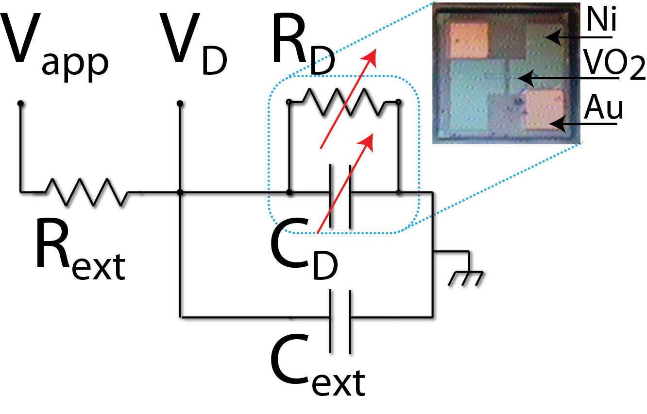
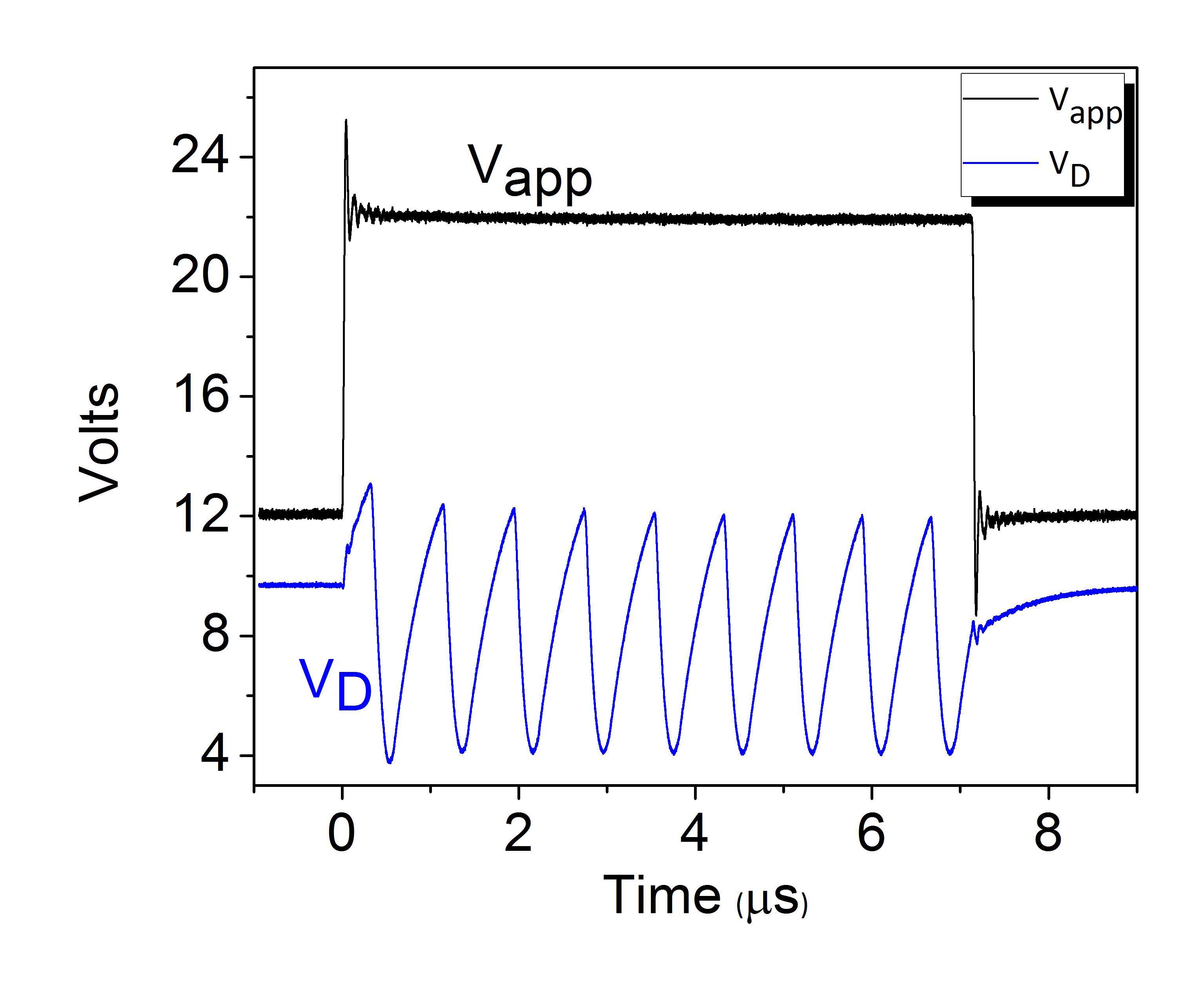
In this configuration, the VO2 device functions essentially as a capacitor with a variable internal shunt resistance RD. The capacitance CD is primarily fixed by device geometry, although variations of the dielectric constant of VO2 throughout the phase transition (such as have been shown in the context of memory-capacitanceDriscoll et al. (2009a); Di Ventra et al. (2009) and VO2 hybrid-metamaterialsDriscoll et al. (2008)) may have small effects - and we discuss this later in Section IV.2. The pre-pulse steady-state starting voltage is VD=VbiasRD/(RD + Rext). At the start of the pulse (t=0), VD increases, following a canonical Resistance-Capacitance (RC) charging curve. Once VD surpasses a threshold voltage (which we will call VD:IMT), it transitions sharply from increasing VD to decreasing. We assign this change to an IMT event occurring in the VO2, which effectively lowers the internal shunt resistance RD of the capacitor. With lower internal resistance, the capacitor undergoes rapid discharge and VD plummets. This discharge continues until VD reaches a lower threshold voltage (VD:MIT at which a second event - which we similarly assign to a a Metal-to-Insulator-Transition (MIT) - restores the high internal device resistance. The process reverses and this sequence of events repeats; alternating charging and discharging between IMT and MIT events with a fairly stable periodicity Kim et al. (2010a).
III Grain-scale model of oscillations.
Our hope is that by developing a model for these observed oscillations, we may gain insight into the driving mechanism behind them. We start with a 2D network of square VO2 grains of differing size, each with total resistivity dependent on its size and its state (metal or insulator)Rozen et al. (2006); Dai et al. (2008). The granularity of polycrystaline VO2 is well documentedPan et al. (2004); Mlyuka and Kivaisi (2006), although the size of grains may vary considerably from one VO2 preparation to another. There is also evidence to suggest the percolation length scales for the IMT may not always coincide with the crystal granularity Kim et al. (2010c); Qazilbash et al. (2011); Frenzel et al. (2009). A cartoon illustrating our model arrangement is shown in Figure 3. The network consists of NixNj grains, and in our model we restrict our investigation to a 50x50 network array to keep computation time manageable.
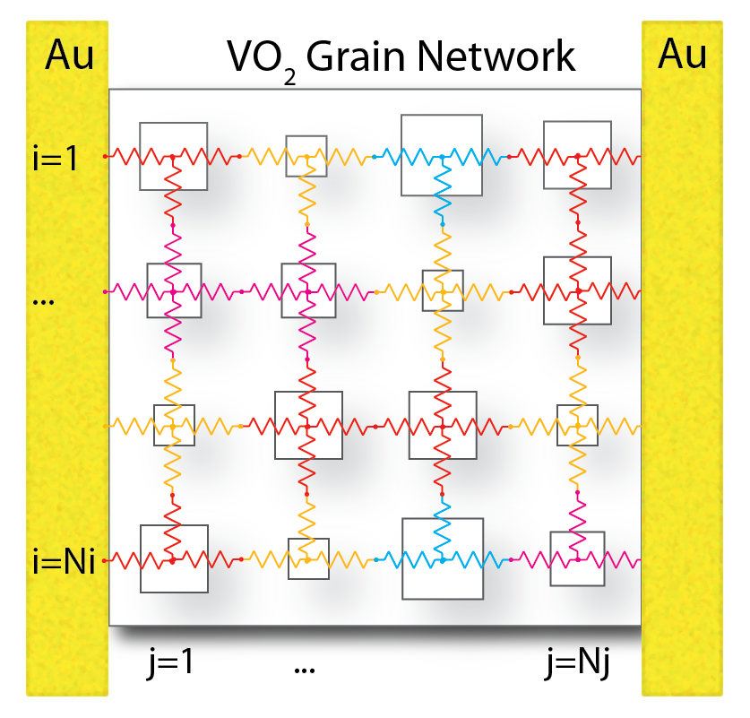
This grain network is placed in an external circuit containing resistance Rext and capacitance Cext, and driven by Vapp, as shown in Figure 1. The circuit differential equation (Equation 1), is solved via Runge-Kutta time-stepping.
| (1) |
At each time-step, we solve for the internal state of the grain network. This includes solving a Kirchoff network problemPoklonski et al. (2006) for the voltage across each grain and the Thevenin effective circuit resistance RD. The other VO2 effective circuit parameter CD is found by a differential capacitance equation (Equation 2) which can be evaluated via a self-consistent Bruggeman effective medium formulation (Equations 3,4)
| (2) | ||||
| (3) | ||||
| (4) |
Superscript i and j are row and column indices for the grains (running to Ni and Nj total). The binary matrix Xij = 1 if the grain i,j is metal and 0 if insulator. is a capacitive fractional-fields factor (the proportion of the device capacitance which involves the VO2 dielectric), which is found via finite element simulation using the COMSOL commercial code package. C0 is a geometrical capacitance which is determined empirically, fitting 1/RC to the capacitive charging curve. External circuit parameters such as Rext and Vapp are taken directly from experimental values. The extrema values for RD(metal) and RD(insulator) are taken from temperature data.
III.1 Thermal triggering
The temperature driven IMT-MIT has been investigated in great detail and we ground our model using experimental data giving resistance as a function of temperature R(T) through the phase transition. This data is shown in Figure 4a, and displays the characteristic sharp change in resistivity around 345K.
Then, in a procedure similar to previous worksSharoni et al. (2008); Kim et al. (2004), we assume each grain will undergo an IMT in response a ”high-threshold” temperature T, and a MIT at a low-threshold T.
| (5) | ||||
| (6) |
We assign a stochastic distribution to the values of and throughout the network, following the Gaussian form
| (7) | |||
| (8) |
The values of T0 and are fit to the experimental R(T) data shown in Figure 4a. From this, we find a variance of K and =.1*T0 reproduces the shape of the IMT fairly well. This fit gives us confidence that we understand the thermal response of VO2, even though our thermal model is simple compared to some previous treatments.
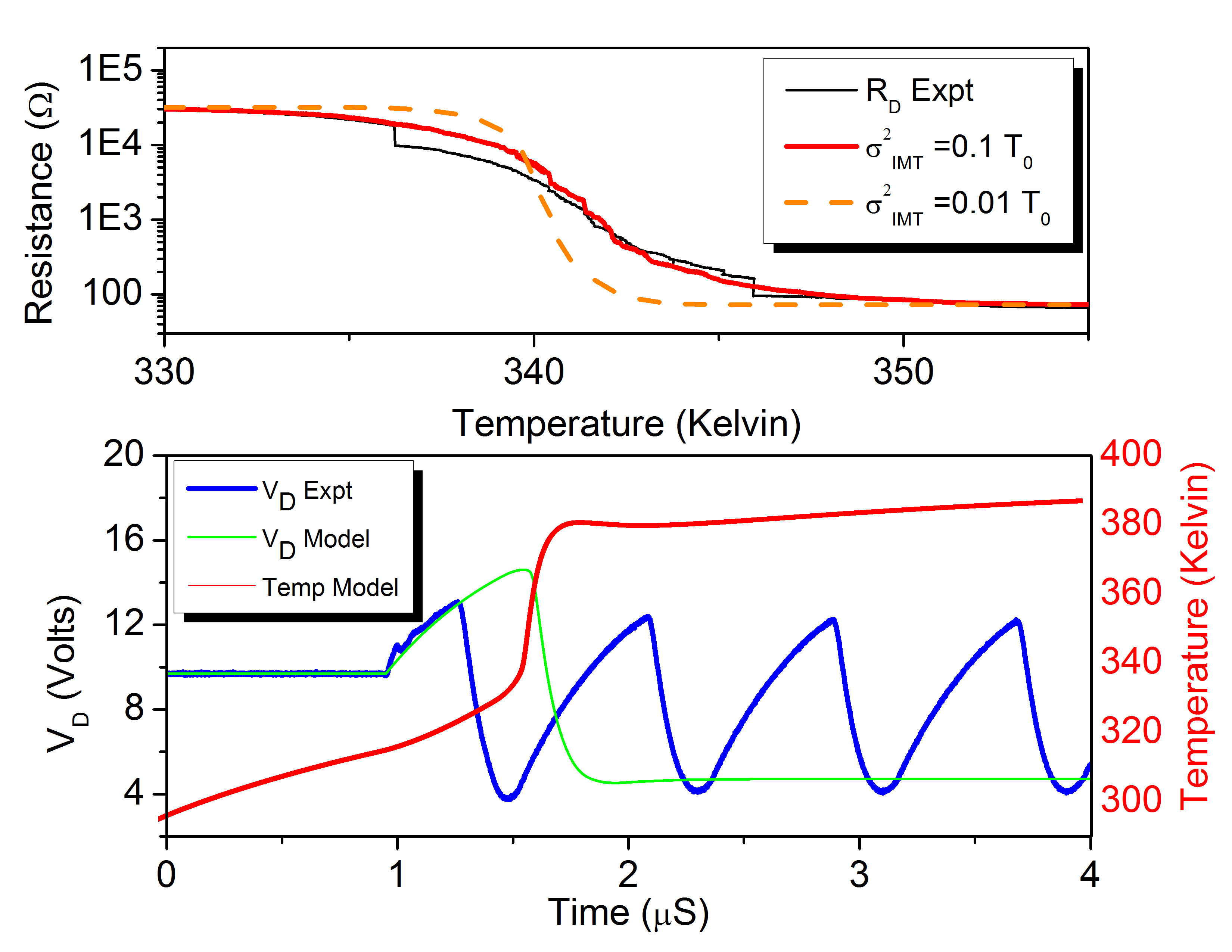
Using this temperature-only-triggered model, we attempt to reproduce the oscillations shown in Figure 2. Our model tracks the power dissipated in each grain and employs a finite-element method to solve for the grain and substrate temperatures as a function of time. Material thermal parameters are taken from literature, and the enthalpy of phase-transition for VO2 is included. Figure 4b re-plots our experimental oscillations in blue, and the model results in green. The result is striking: although we can track for a short while, we are unable to produce any oscillatory phenomena.
Generalizing the behavior that prohibits oscillations, thermal-initiated IMTs exhibit a runaway behavior rather than the self-stabilizing oscillatory nature seen in Figure 2. This is apparent in the average VO2 grain temperature plot (red) of 4b. Note that although individual different grains may attain different temperatures over the course of oscillations, such gradients equalize quickly within the network. Average temperature remains a fairly accurate and easily visualized metric of the VO2 oscillation thermodynamics. As the thermally-triggered IMT occurs, VO2 temperature skyrockets even while VD discharges. Once the temperature of the discharged device has surpassed , there is no way for it to cool thereafter. Power dissipation and temperature both settle towards steady-state with the device firmly in the metallic state. The causes of this process will become more apparent as we discuss thermal dynamics in Section III.4.
III.2 Electrical triggering
With the failure of a temperature-only-triggering model to produce oscillations, and following insights from previous work on voltage-induced effects in VO2,Sharoni et al. (2008); Ruzmetov et al. (2009); Stefanovich et al. (2000); Lee et al. (2008) we now introduce an electric-field driven transition. To do this, we also assign a voltage drop at which each grain undergoes phase transition V and V. We again use random values from a normal distribution as we did for T and T.
| (9) | |||
| (10) |
We lack direct data to which to fit these distributions (as we did in Figure 4a). Thus, we retain the same value for the variance found in above, =0.1*V0. From an energetics perspective, this makes a great deal of sense - both distributions are surely tied to the same underlying Mott-physics. V0 remains a fitting parameter in our model.
As we have not removed possible thermal triggering, the conditions for grain transition can now be stated as:
| (11) | ||||
| (12) |
This combined triggering criterion reproduces both the waveshape and periodicity of the experimentally observed oscillations quite well. In Figure 5, we re-plot the experimental data from Figure 2 in blue, and numerical results from our model are shown overlaid in green.
III.3 Voltage-temperature dependence
Although section III.2 demonstrated voltage is the primary trigger, device temperature still plays a role in oscillations. There is a known dependence of oscillation amplitude on device temperatureKim et al. (2010b). If we look carefully at the data in Figure 5, we notice a subtle decay envelope to the amplitude of the VIMT oscillation peaks. We believe this envelope is caused by a thermalization of the device on a multi-oscillation timescale. To accommodate this, we include a temperature-dependence to the IMT transition voltage as
| (13) |
where T0=295oK. is a liner temperature coefficient, the fitting of which we discuss below. Without including this voltage-temperature interplay, our model quickly loses sync with the experimental data over the course of several oscillation periods. This thermalization envelope is most clearly observed over a long pluse, and experimental data (solid blue) for a 100s pulse is shown in Figure 6. For clarity in this figure, the bottom half of the oscillations is omitted from view (interestingly, we observe no envelope of VMIT).
Using the data from Figure 6 combined with our thermal-finite element model, we can fit a value for . Overlaid on the experimental data (dashed line) is this fit, which gives x. This value of is used in our oscillation model.
Explanation of this a long time-scale thermalization is straightforward. Although locally the VO2 film may heat or cool quite quickly in response to current through its volume, the 500m thick sapphire substrate is comparatively massive. The large thermal inertia of the substrate smooths out oscillatory heating away from the film; and when heated only from the top the substrate can require tens of micro-seconds to reach a steady-state temperature gradient.
III.4 Temperature dynamics
In the above Section III.3 we have discussed the critical interplay between temperature and voltage-triggering, showing how a long multi-oscillation timescale thermalization envelopes the oscillation amplitude. In this section, we look closer at the temperature evolution on the timescale of the oscillation period.
To begin, in Figure 7 we plot the average grain temperature (red) during oscillations along with (green) - both from our model. Looking at Figure 7 quantitatively, we notice that the average temperature reached is not sufficient to trigger oscillations. Although the peak average temperature during the discharge cycle of the oscillation comes close to reaching TIMT, a thermal-driving event would have to occur at-or-before the peak in VD. The model results indicate that the device is well below TIMT when VD:IMT is reached. The temperature range in Figure 7 agrees fairly well with previous numerical work on the subject Gopalakrishnan et al. (2009), and our own investigations using commercial finite element package COMSOL. Compared to COMSOL, our home-grown finite-element code over-estimates temperatures reached - perhaps due to difficulty in modeling all of the spatially massive substrate (this is not an issue for commercial packages such as COMSOL). However, commercial codes cannot be run from within Runge-Kutta time-stepping of equation 1, and our code thus critically allows us to calculate temperature dynamics during oscillations.
Although a quantitative argument for non-thermal triggering seems compelling, we are acutely aware that precisely solving for temperature can be difficult in such nanoscale systems. Material properties can differ from published bulk values, and interface effects can dominate transport and heatingDi Ventra (2008). As we look closely though, the power dissipation in the device also appears qualitatively unfit to explain the oscillations. A thermally-driven transition would have to follow the logical sequence:
-
I
The insulating device heats with applied VD until it reaches TIMT, where it undergoes an IMT (becoming metallic).
-
II
The metallic device discharges its stored capacitive energy through the its own volume - cooling as it discharges - until it reaches TMIT where it undergoes MIT (becoming insulating).
-
III
The process repeats.
However, Figure 7 illustrates that region II which occurs after VD:IMT is a region of maximum power dissipation; a region of heating not cooling. A simple ohms-law argument explains: Just before and just after the IMT, VD is approximately VD:IMT. However, the resistance RD has changed by a factor of 10, and thus the power dissipated (P=V/RD) is substantially greater during region II than during region I. Thus, we come to the conclusion that a purely-thermal explanation for the oscillations is qualitatively as well as quantitatively mismatched to experimental data.
Summarizing Section III, we have identified voltage as a key player in triggering observed oscillations on the grounds of several thermal arguments. One interesting question then is whether electrostatic voltage may also trigger the also IMT in a current-free (ie. FET) configuration. The joule-heating present in our two-terminal device complicates matters, in light of the voltage/temperature interplay identified in Section III.3. Previous work has suggested such electrostatic switching can exist,Chudnovskiy et al. (2002); Qazilbash et al. (2008b); Kim et al. (2004) although these early results await further confirmation. Exploring the phase-space defined by the interplay of temperature, electrostatic field, and current in these VO2 oscillations may reveal information about the correlated electron dynamics and energy scales associated with the Mott-transition.
IV Percolation
In this section, we go into further detail on the mechanisms of the IMT and MIT transitions. Polycrystalline VO2 is known to exhibit percolative behavior during phase transitionQazilbash et al. (2007, 2011); Sharoni et al. (2008); Wu et al. (2011), and this has interesting effects on a voltage-triggered transition. Using the model from Section III which accurately predicts the observed electrical oscillations, we attempt to gain insight on several of the internal processes during oscillatory events.
IV.1 Percolative avalanche driven oscillations
In several previous worksSharoni et al. (2008); Ram’irez et al. (2009), avalanche-like MIT and IMT transitions have been observed under the right conditions. The immediacy of the observed change from charging to discharging in our oscillations leads us to suspect similar avalanche behavior in our electrically-driven device. Examining the details of our model, we see that the voltage drop across any grain in the network (see Figure 3) is proportional to the resistance of the grain. During the charging cycle of the waveform voltage across the entire device (VD) increases, and Vij across each grain does as well. This charging continues until one ”unlucky” grain hits its V first. Because the grains receive a stochastic distribution for V (see Equation 9), this can be a random grain anywhere in the network. In experiments, it is seen that the phase-transition is often seeded at particular places such as defects or boundaries.
The unlucky grain that first hits its IMT trigger condition undergoes an IMT. Once this grain becomes metallic, it supports a lower voltage drop (Rins/R 20) - which shifts much of its voltage burden to neighboring grains. The neighboring grains in turn become increasingly likely to undergo their own IMT events. The IMT spreads across the entire sample in an avalanche-like manner. This process is depicted in Figure 8a for a network of 50x50 grains. The upper sequence of black and white frames shows whether each grain is insulating (white) or metallic (black). The lower color frames depict the voltage drop across each grain. The neighbor-neighbor grain interaction, mediated by voltage drop is quite evident.
As is common in percolative systems, the Thevenin resistance RD of the network is quite sensitive to the spatial distribution of triggered grains. The device resistivity RD is shown above each frame in the sequence of Figure 8, and we see the largest drop occurs in frames #6 and 7, where the percolation path is completed from left to right. Once a conducting path forms plummets, and VD begins to drop as the device discharges.
During discharge, there comes a point where VD drops far enough that a similar process happens in reverse. This MIT is depicted in Figure 8b. However, the MIT process is not exactly the reverse of the IMT. The equations governing resistors in parallel tend to ”favor” low-resistances in the following manner: Decreasing the value of one resistor (in a parallel network) lowers the Thevenin resistance significantly, but raising the value of a single resistor has only a little effect on the Thevenin resistance. For this reason, the avalanche-like behavior observed in Figure 8a is not seen in Figure 8b. Instead, the process much more closely resembles random percolation, with only moderate neighbor-neighbor interaction. This difference in the mechanisms between IMT and MIT may explain the difference in sharpness of the transitions at V and V observed in experiments.Kim et al. (2010a)
IV.2 Effective medium effects
The percolative nature of the VO2 phase transition allows for an inhomogeneous intermediate state where both metallic and insulating VO2 coexist. The dielectric constants of metal and insulating phase VO2 are distinct; and when both phases can be present in a composite it leads to interesting properties. The average response of the inhomogeneous sample is described by an effective medium, and can have radically different values than either. This leads to quite interesting and novel effects. For example, the inhomogeneity Qazilbash et al. (2007); Frenzel et al. (2009) of polycrystalline VO2 mid-transition is responsible for observed memristance Driscoll et al. (2009b) and memory-capacitance Driscoll et al. (2009a); Di Ventra et al. (2009).
The same memory-capacitance as reported in Driscoll et al. (2009a) has previously been attributed as playing a key role in voltage-controlled oscillations in VO2Kim et al. (2010a). This is a question we are situated to investigate in more depth using our model. To look closely at the effects of capacitance on the oscillations, we focus attention on a single IMT transition event. In Figure 9, we plot CD(t) (as calculated from equations 2-4), along with the familiar VD and RD.
Looking at Figure 9, as VO2 transitions from insulating to metallic at the IMT, RD drops monotonically to its metallic-state value. The capacitance CD, however, briefly increases before also decreasing to its metallic-state value. This increase is due to the coexistence of metallic and insulating grains, and is predicted by effective medium (Equation 4). However, as Figure 9 shows, the increase in CD is a small effect, and is contained to a short timespan near the start of the IMT. This leads us to believe the effective medium behavior of CD has only a minor influence on the shape of the oscillations, and is not a primary driver. We observe the same increase in CD at the MIT transition edge, but it also is too small and short-lived an effect to bear responsibility for the oscillations.
V Summary
In this work, we have discussed the thermal and electrical driving mechanisms behind observed oscillations occurring in VO2 films. In addition to experimentally confirming the oscillations reported by Y.W. Lee et.al.Lee et al. (2008), we have compiled a numerical model which is able to replicate and explain these oscillations in terms of an voltage-triggered Insulator-to-Metal phase-transition. Temperature is known to trigger the IMT in VO2, and temperature plays some role in the shape of the oscillations. However, we find that temperature-only triggering cannot explain oscillations. This result is likely of great importance for applications of these oscillations, as repeated thermal-cycling typically appreciably shortens device lifetime.
One question that remains unaddressed is the role, if any, of the structural phase transition in an electric-field triggered transition. The temperature driven IMT in VO2 exhibits a structural transition that happens concurrent with the electronic reconfiguration. However, there is evidence Qazilbash et al. (2011, 2007); Kim et al. (2004); Arcangeletti et al. (2007); Wei et al. (2009); Yao et al. (2010); Kim et al. (2007, 2008, 2005) to suggest the electronic and structural transitions are not necessarily linked, but merely overlaid. This structural electronic decoupling suggests the electronic correlations in VO2 play an important role in the IMT phase transition.
Studies which probe the crystal structure simultaneous with these oscillations have not yet been reported - likely because the time and length scales associated with the VO2 oscillator devices greatly complicate experiments such as x-ray diffraction. However, as mentioned in the introduction (Section I) the question of whether or not the structural transition occurs has great implications about the longevity of these devices. In many applications, devices could easily be expected to perform 1012 to 1014 oscillation events over their lifetime, a likely impossibility if crystallographic changes are occurring. An evident goal for the new future is to experimentally investigate the existence of structural transition in oscillations in the near future.
VI Acknowledgments
T.D. acknowledges support from an IC postdoctoral fellowship. M.D. acknowledges partial support from NSF. This research is supported by AFOSR and ETRI
VII References
References
- Morin [1959] F J Morin. Oxides which show a metal-to-insulator transition at the neel temperature. Physical Review Letters, 3(1):34–36, 1959.
- Qazilbash et al. [2007] Mumtaz M. Qazilbash, Markus Brehm, Byung-Gyu Chae, P.-C. Ho, Gregory O. Andreev, Bong-Jun Kim, Sun Jin Yun, A.V. Balatsky, M.B. Maple, Fritz Keilmann, Hyun-Tak Kim, and Dimitri N. Basov. Mott Transition in VO2 revealed by Infrared Spectroscopy and Nano-Imaging. Science, 318(December):1750–1753, 2007.
- Qazilbash et al. [2008a] Mumtaz M. Qazilbash, AA Schafgans, KS Burch, SJ Yun, BG Chae, BJ Kim, Hyun-Tak Kim, and DN Basov. Electrodynamics of the vanadium oxides VO2 and V2O3. Physical Review B, 77(115121), 2008a. doi: 10.1103/PhysRevB.77.115121. URL http://arxiv.org/abs/0803.2739.
- Liu et al. [2009] M. Liu, B. Pardo, MM Qazilbash, S.J. Yun, BG Chae, BJ Kim, DN Basov, and RD Averitt. Conductivity dynamics in the correlated metallic state of V2O3. In Lasers and Electro-Optics, 2009 and 2009 Conference on Quantum electronics and Laser Science Conference. CLEO/QELS 2009. Conference on, volume 4, pages 1–2. IEEE, 2009. URL http://ieeexplore.ieee.org/xpls/abs_all.jsp?arnumber=5225800.
- Zylbersztejn and Mott [1975] A. Zylbersztejn and N.F. Mott. Metal-insulator transition in vanadium dioxide. Physical Review B, 11(11):4383, 1975.
- Kim et al. [2004] Hyun-Tak Kim, B G Chae, D H Youn, S L Maeng, G Kim, K Y Kang, and Y S Lim. Mechanism and observation of Mott transition in VO 2 based two- and three-terminal devices. New Journal of Physics, 6:52–70, 2004.
- Rice et al. [1994] T.M. Rice, H. Launois, and J.P. Pouget. Comment on ”VO2: Peierls or Mott-Hubbard? A View from Band Theory”. Physical Review Letters, 73(22):9007–9007, 1994.
- Wentzcovitch et al. [1994] Renata M Wentzcovitch, Werner W Schulz, and Philip B Allen. VO2: Peierls or Mott-Hubbard? A View from Band Theory. Physical Review Letters, 72(21):3389–3392, 1994.
- Cavalleri et al. [2004] Andrea Cavalleri, Th. Dekorsy, H. Chong, J. Kieffer, and R. Schoenlein. Evidence for a structurally-driven insulator-to-metal transition in VO2: A view from the ultrafast timescale. Physical Review B, 70(16):3–6, October 2004. ISSN 1098-0121. doi: 10.1103/PhysRevB.70.161102. URL http://link.aps.org/doi/10.1103/PhysRevB.70.161102.
- Cavalleri et al. [2001] Andrea Cavalleri, Cs. Tóth, C W Siders, J A Squier, F Ráksi, P Forget, and J C Kieffer. Femtosecond structural dynamics in VO 2 during an ultrafast solid-solid phase transition. PRL, 87237401:1–4, 2001.
- Rini et al. [2005] Matteo Rini, Andrea Cavalleri, Robert W Schoenlein, René López, Leonard C Feldman, Richard F Haglund, Lynn A Boatner, and Tony E Haynes. Photoinduced phase transition in VO 2 nanocrystals : control of surface-plasmon resonance ultrafast. Optics Letters, 30(5):1–3, 2005.
- Lysenko et al. [2006] S Lysenko, AJ Rua, V Vikhnin, J Jimenez, F Fernandez, and H Liu. Light-induced ultrafast phase transitions in VO2 thin film. Applied surface science, 252(15):5512–5515, 2006. doi: 10.1016/j.apsusc.2005.12.137. URL http://linkinghub.elsevier.com/retrieve/pii/S0169433205018027.
- Lopez et al. [2004] René Lopez, L. a. Boatner, T. E. Haynes, R. F. Haglund, and L. C. Feldman. Switchable reflectivity on silicon from a composite VO[sub 2]-SiO[sub 2] protecting layer. Applied Physics Letters, 85(8):1410, 2004. ISSN 00036951. doi: 10.1063/1.1784546. URL http://link.aip.org/link/APPLAB/v85/i8/p1410/s1&Agg=doi.
- Driscoll et al. [2008] Tom Driscoll, S Palit, Mumtaz M. Qazilbash, Markus Brehm, Fritz Keilmann, Byung-Gyu Chae, Sun-Jin Yun, Hyun-Tak Kim, Nan Marie Jokerst, David R. Smith, and Dimitri N. Basov. Dynamic tuning of an infrared hybrid-metamaterial resonance using vanadium dioxide. Applied Physics Letters, 93(024101), 2008. doi: 10.1063/1.2956675. URL http://ieeexplore.ieee.org/xpls/abs_all.jsp?arnumber=4838777.
- Driscoll et al. [2009a] Tom Driscoll, Hyun-Tak Kim, Byung-Gyu Chae, Bong-Jun Kim, Yong-Wook Lee, Nan Marie Jokerst, S Palit, David R. Smith, Massimiliano Di Ventra, and Dimitri N. Basov. Memory metamaterials. Science (New York, N.Y.), 325(5947):1518–21, September 2009a. ISSN 1095-9203. doi: 10.1126/science.1176580. URL http://www.ncbi.nlm.nih.gov/pubmed/19696311.
- Dicken et al. [2009] Matthew J Dicken, Koray Aydin, Imogen M Pryce, Luke A Sweatlock, M Boyd, Sameer Walavalkar, James Ma, and Harry A Atwater. Frequency tunable near-infrared metamaterials based on VO 2 phase transition. Optics Express, 17(20):295–298, 2009.
- Kim et al. [2006] B.J. Kim, Y.W. Lee, B.G. Chae, S.J. Yun, S.Y. Oh, Y.S. Lim, and Hyun-Tak Kim. Temperature dependence of Mott transition in VO_2 and programmable critical temperature sensor. Arxiv preprint cond-mat/0609033, 009033v1, 2006. URL http://arxiv.org/abs/cond-mat/0609033.
- Driscoll et al. [2010] Tom Driscoll, J. Quinn, S. Klein, Hyun-Tak Kim, B. J. Kim, Yuriy V. Pershin, Massimiliano Di Ventra, and D. N. Basov. Memristive adaptive filters. Applied Physics Letters, 97(9):093502, 2010. ISSN 00036951. doi: 10.1063/1.3485060. URL http://link.aip.org/link/APPLAB/v97/i9/p093502/s1&Agg=doi.
- Driscoll et al. [2009b] Tom Driscoll, Hyun-Tak Kim, B.G. Chae, Massimiliano Di Ventra, and DN Basov. Phase-transition driven memristive system. Applied Physics Letters, 95(4):043503, 2009b. URL http://link.aip.org/link/?APPLAB/95/043503/1.
- Pershin [2011] YV Pershin. Memory effects in complex materials and nanoscale systems. Advances in Physics, 00(00):1–71, 2011. doi: 10.1080/0001873YYxxxxxxxx. URL http://www.tandfonline.com/doi/abs/10.1080/00018732.2010.544961.
- Crunteanu et al. [2010] Aurelian Crunteanu, Julien Givernaud, Jonathan Leroy, David Mardivirin, Corinne Champeaux, Jean-Christophe Orlianges, Alain Catherinot, and Pierre Blondy. Voltage- and current-activated metal–insulator transition in VO 2 -based electrical switches: a lifetime operation analysis. Science and Technology of Advanced Materials, 11(6):065002, December 2010. ISSN 1468-6996. doi: 10.1088/1468-6996/11/6/065002. URL http://stacks.iop.org/1468-6996/11/i=6/a=065002?key=crossref.3559a62a92655ee932bf6fc313bbb47a.
- Lee et al. [2008] Y.W. Lee, B.J. Kim, J.W. Lim, S.J. Yun, Sungyoul Choi, B.G. Chae, G. Kim, and Hyun-Tak Kim. Metal-insulator transition-induced electrical oscillation in vanadium dioxide thin film. Applied Physics Letters, 92(16):162903, 2008. doi: 10.1063/1.2911745. URL http://link.aip.org/link/?APPLAB/92/162903/1.
- Sakai [2008] Joe Sakai. High-efficiency voltage oscillation in VO[sub 2] planer-type junctions with infinite negative differential resistance. Journal of Applied Physics, 103(10):103708, 2008. ISSN 00218979. doi: 10.1063/1.2930959. URL http://link.aip.org/link/JAPIAU/v103/i10/p103708/s1&Agg=doi.
- Kim et al. [2010a] Hyun-Tak Kim, Bong-Jun Kim, Sungyoul Choi, Byung-Gyu Chae, Yong Wook Lee, Tom Driscoll, Mumtaz M. Qazilbash, and D. N. Basov. Electrical oscillations induced by the metal-insulator transition in VO[sub 2]. Journal of Applied Physics, 107(2):023702, 2010a. ISSN 00218979. doi: 10.1063/1.3275575. URL http://link.aip.org/link/JAPIAU/v107/i2/p023702/s1&Agg=doi.
- Kim et al. [2010b] B.J. Kim, Giwan Seo, Y.W. Lee, Sungyoul Choi, and Hyun-Tak Kim. Linear Characteristics of a Metal–Insulator Transition Voltage and Oscillation Frequency in VO2 Devices. Electron Device Letters, IEEE, 31(11):1314–1316, 2010b. URL http://ieeexplore.ieee.org/xpls/abs_all.jsp?arnumber=5595090.
- Sharoni et al. [2008] Amos Sharoni, J.G. Ram’irez, and I.K. Schuller. Multiple avalanches across the metal-insulator transition of vanadium oxide nanoscaled junctions. Physical review letters, 101(2):26404, 2008. doi: 10.1103/PhysRevLett.101.026404. URL http://link.aps.org/doi/10.1103/PhysRevLett.101.026404.
- Ram’irez et al. [2009] J.G. Ram’irez, Amos Sharoni, Y Dubi, ME Gomez, and I.K. Schuller. First-order reversal curve measurements of the metal-insulator transition in VO2: Signatures of persistent metallic domains. Physical Review B, 79(23):235110, 2009. doi: 10.1103/PhysRevB.79.235110. URL http://prb.aps.org/abstract/PRB/v79/i23/e235110.
- Di Ventra et al. [2009] Massimiliano Di Ventra, Yuriy V. Pershin, and Leon O. Chua. Circuit elements with memory: memristors, memcapacitors and meminductors. Proceedings of the IEEE, 97(8):1371–1372, January 2009. doi: 10.1109/JPROC.2009.2021077. URL http://arxiv.org/abs/0901.3682.
- Rozen et al. [2006] John Rozen, René Lopez, Richard F. Haglund, and Leonard C. Feldman. Two-dimensional current percolation in nanocrystalline vanadium dioxide films. Applied Physics Letters, 88(8):081902, 2006. ISSN 00036951. doi: 10.1063/1.2175490. URL http://link.aip.org/link/APPLAB/v88/i8/p081902/s1&Agg=doi.
- Dai et al. [2008] Jun Dai, Xingzhi Wang, Ying Huang, and Xinjian Yi. Modeling of temperature-dependent resistance in micro- and nanopolycrystalline VO[sub 2] thin films with random resistor networks. Optical Engineering, 47(3):033801, 2008. ISSN 00913286. doi: 10.1117/1.2894146. URL http://link.aip.org/link/OPEGAR/v47/i3/p033801/s1&Agg=doi.
- Pan et al. [2004] Mei Pan, Hongmei Zhong, Shaowei Wang, Jie Liu, Zhifeng Li, Xiaoshuang Chen, and Wei Lu. Properties of VO 2 thin film prepared with precursor VO ( acac ) 2. Journal of Crystal Growth, 265:121–126, 2004. doi: 10.1016/j.jcrysgro.2003.12.065.
- Mlyuka and Kivaisi [2006] N. R. Mlyuka and R. T. Kivaisi. Correlation between optical, electrical and structural properties of vanadium dioxide thin films. Journal of Materials Science, 41(17):5619–5624, June 2006. ISSN 0022-2461. doi: 10.1007/s10853-006-0261-y. URL http://www.springerlink.com/index/10.1007/s10853-006-0261-y.
- Kim et al. [2010c] Jeehoon Kim, Changhyun Ko, Alex Frenzel, Shriram Ramanathan, and Jennifer E. Hoffman. Nanoscale imaging and control of resistance switching in VO[sub 2] at room temperature. Applied Physics Letters, 96(21):213106, 2010c. ISSN 00036951. doi: 10.1063/1.3435466. URL http://link.aip.org/link/APPLAB/v96/i21/p213106/s1&Agg=doi.
- Qazilbash et al. [2011] Mumtaz M. Qazilbash, a. Tripathi, a. Schafgans, Bong-Jun Kim, Hyun-Tak Kim, Zhonghou Cai, M. Holt, J. Maser, F. Keilmann, O. Shpyrko, and D. Basov. Nanoscale imaging of the electronic and structural transitions in vanadium dioxide. Physical Review B, 83(16):1–7, April 2011. ISSN 1098-0121. doi: 10.1103/PhysRevB.83.165108. URL http://link.aps.org/doi/10.1103/PhysRevB.83.165108.
- Frenzel et al. [2009] Alex. Frenzel, Mumtaz M. Qazilbash, M. Brehm, Byung-Gyu Chae, Bong-Jun Kim, Hyun-Tak Kim, A. Balatsky, F. Keilmann, and D. Basov. Inhomogeneous electronic state near the insulator-to-metal transition in the correlated oxide VO2. Physical Review B, 80(11):1–7, September 2009. ISSN 1098-0121. doi: 10.1103/PhysRevB.80.115115. URL http://link.aps.org/doi/10.1103/PhysRevB.80.115115.
- Poklonski et al. [2006] N. a. Poklonski, a. a. Kocherzhenko, a. I. Benediktovitch, V. V. Mitsianok, and a. M. Zaitsev. Simulation of dc conductance of two-dimensional heterogeneous system: application to carbon wires made by ion irradiation on polycrystalline diamond. Physica Status Solidi (B), 243(6):1212–1218, May 2006. ISSN 0370-1972. doi: 10.1002/pssb.200541079. URL http://doi.wiley.com/10.1002/pssb.200541079.
- Ruzmetov et al. [2009] Dmitry Ruzmetov, Gokul Gopalakrishnan, Jiangdong Deng, V. Narayanamurti, and Shriram Ramanathan. Electrical triggering of metal-insulator transition in nanoscale vanadium oxide junctions. Journal of Applied Physics, 106(8):083702–083702, 2009. doi: 10.1063/1.3245338. URL http://ieeexplore.ieee.org/xpls/abs_all.jsp?arnumber=5292009.
- Stefanovich et al. [2000] G. Stefanovich, A Pergament, and D Stefanovich. Electrical switching and Mott transition in VO2. Journal of Physics: Condensed Matter, 12:8837, 2000. URL http://iopscience.iop.org/0953-8984/12/41/310.
- Gopalakrishnan et al. [2009] Gokul Gopalakrishnan, D. Ruzmetov, and Shriram Ramanathan. On the triggering mechanism for the metal–insulator transition in thin film VO 2 devices: electric field versus thermal effects. Journal of materials science, 44(19):5345–5353, 2009. doi: 10.1007/s10853-009-3442-7. URL http://www.springerlink.com/index/7U24554G53291604.pdf.
- Di Ventra [2008] Massimiliano Di Ventra. Electrical transport in nanoscale systems. Cambridge University Press, Cambridge, 2008.
- Chudnovskiy et al. [2002] Feliks Chudnovskiy, Serge Luryi, and Boris Spivak. Switching device based on first-order metal- insulator transition induced by external electric field. Future Trends in Microelectronics: the Nano Millennium, pages 148–155, 2002.
- Qazilbash et al. [2008b] Mumtaz M. Qazilbash, Z. Q. Li, V. Podzorov, M. Brehm, F. Keilmann, B. G. Chae, Hyun-Tak Kim, and D. N. Basov. Electrostatic modification of infrared response in gated structures based on VO[sub 2]. Applied Physics Letters, 92(24):241906, 2008b. ISSN 00036951. doi: 10.1063/1.2939434. URL http://link.aip.org/link/APPLAB/v92/i24/p241906/s1&Agg=doi.
- Wu et al. [2011] Tai-Lung Wu, Luisa Whittaker, Sarbajit Banerjee, and G. Sambandamurthy. Temperature and voltage driven tunable metal-insulator transition in individual WxV1-xO2 nanowires. Physical Review B, 83(7):2–5, February 2011. ISSN 1098-0121. doi: 10.1103/PhysRevB.83.073101. URL http://link.aps.org/doi/10.1103/PhysRevB.83.073101.
- Arcangeletti et al. [2007] E. Arcangeletti, L. Baldassarre, D. Di Castro, S. Lupi, L. Malavasi, C. Marini, a. Perucchi, and P. Postorino. Evidence of a Pressure-Induced Metallization Process in Monoclinic VO2. Physical Review Letters, 98(19):1–4, May 2007. ISSN 0031-9007. doi: 10.1103/PhysRevLett.98.196406. URL http://link.aps.org/doi/10.1103/PhysRevLett.98.196406.
- Wei et al. [2009] Jiang Wei, Zenghui Wang, Wei Chen, and D.H. Cobden. New aspects of the metal–insulator transition in single-domain vanadium dioxide nanobeams. Nature Nanotechnology, 4(7):420–424, 2009. doi: 10.1038/NNANO.2009.141. URL http://www.nature.com/nnano/journal/v4/n7/abs/nnano.2009.141.html.
- Yao et al. [2010] Tao Yao, Xiaodong Zhang, Zhihu Sun, Shoujie Liu, Yuanyuan Huang, Yi Xie, Changzheng Wu, Xun Yuan, Wenqing Zhang, Ziyu Wu, Guoqiang Pan, Fengchun Hu, Lihui Wu, Qinghua Liu, and Shiqiang Wei. Understanding the Nature of the Kinetic Process in a VO2 Metal-Insulator Transition. Physical Review Letters, 105(22):2–5, November 2010. ISSN 0031-9007. doi: 10.1103/PhysRevLett.105.226405. URL http://link.aps.org/doi/10.1103/PhysRevLett.105.226405.
- Kim et al. [2007] Bong-Jun Kim, Yong Wook Lee, Byung-Gyu Chae, Sun Jin Yun, Soo-Young Oh, Hyun-Tak Kim, and Yong-Sik Lim. Temperature dependence of the first-order metal-insulator transition in VO[sub 2] and programmable critical temperature sensor. Applied Physics Letters, 90(2):023515, 2007. ISSN 00036951. doi: 10.1063/1.2431456. URL http://link.aip.org/link/APPLAB/v90/i2/p023515/s1&Agg=doi.
- Kim et al. [2008] Bong-Jun Kim, Yong Lee, Sungyeoul Choi, Jung-Wook Lim, Sun Yun, Hyun-Tak Kim, Tae-Ju Shin, and Hwa-Sick Yun. Micrometer x-ray diffraction study of VO2 films: Separation between metal-insulator transition and structural phase transition. Physical Review B, 77(23):1–5, June 2008. ISSN 1098-0121. doi: 10.1103/PhysRevB.77.235401. URL http://link.aps.org/doi/10.1103/PhysRevB.77.235401.
- Kim et al. [2005] Hyun-Tak Kim, Byung-Gyu Chae, Doo-Hyeb Youn, Gyungock Kim, Kwang-Yong Kang, Seung-Joon Lee, Kwan Kim, and Yong-Sik Lim. Raman study of electric-field-induced first-order metal-insulator transition in VO[sub 2]-based devices. Applied Physics Letters, 86(24):242101, 2005. ISSN 00036951. doi: 10.1063/1.1941478. URL http://link.aip.org/link/APPLAB/v86/i24/p242101/s1&Agg=doi.