Mesoscopic Thermovoltage Measurement Design
Abstract
Quantitative thermoelectric measurements in the mesoscopic regime require accurate knowledge of temperature, thermovoltage, and device energy scales. We consider the effect of a finite load resistance on thermovoltage measurements of InAs/InP heterostructure nanowires. Load resistance and ac attenuation distort the measured thermovoltage therefore complicating the evaluation of device performance. Understanding these effects improves experimental design and data interpretation.
Keywords:
thermovoltage, quantum dot, nanowire:
73.63.Kv, 05.70.Ln, 07.20.PeTouted for their ability to optimize electronic properties while simultaneously reducing phononic losses, nanostructure materials have advanced the thermoelectric performance benchmark beyond what is possible with bulk materials. As a result, many of the underlying mesoscopic processes responsible for the observed improvements in thermoelectric performance–such as phonon scattering Hochbaum, et al. (2008), phonon drag Boukai, et al. (2008); Chickering, et al. (2009), and electron energy filtering Humphrey, et al. (2002); Kim, et al. (2009)–are now popular topics in fundamental physics research. The goal of this research is to provide quantitative understanding of mesoscopic effects and ultimately improve thermoelectric device design. From an electronic perspective, a quantum dot (QD) is an appealing test platform due to its strong energy modulation and tunability. Here we discuss the influence of a finite load resistance in series with a thermally biased QD defined in an InAs nanowire.
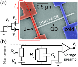
The experimental device is an InAs/InP heterostructure nanowire grown using chemical beam epitaxy and is roughly 50 nm in diameter and 1 m long (see Fig. 1a). The InAs quantum dot is created by introducing two InP barriers during the growth process. The nanowire rests on a wafer with a 100 nm insulating SiO capping layer above n-doped Si, which operates as a global back-gate. Ohmic Ni/Au electrical contacts are defined at both ends of the nanowire using electron beam lithography. The temperature difference across the quantum dot, , is provided by Joule heating generated by an ac heating current at frequency (see Fig. 1a). Further details regarding the application and detection of can be found elsewhere Hoffmann, et al. (2009); Hoffmann and Linke (2009). Thermovoltage is detected using a voltage preamplifier by measuring either the frequency-doubled signal with a lock-in amplifier or by measuring a time-averaged dc signal, see Fig. 1b. The lock-in technique provides a better signal-to-noise ratio than the dc technique, but suffers from attenuation owing to the large resistances in the system and the finite load capacitance, , that exists in the cryostat wiring and filtering. For example, with an off-resonance nanowire resistance of M and nF, which is typical for our setup, the cutoff frequency is Hz. Therefore, we measure dc thermovoltage to avoid attenuation effects.
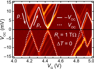
When measuring thermovoltage, the hot electrochemical potential is grounded (by the heating circuit) so that while the cold electrochemical potential, , is allowed to float arbitrarily so that the nanowire can find its equilibrium thermovoltage, . Ideally, is measured using a voltage preamplifier (FEMTO DLPVA-100-F series) with a large input impedance of 1 T, which separates from the preamplifier. However, the global back-gate, at voltage , complicates the measurement. and are capacitively coupled, and therefore influences . For example, when measuring the isothermal open-circuit voltage, , suppose is in resonance with a QD level at energy . When increases, decreases (as do the QD energy levels) until , at which point begins to increase as electrons flow through the QD from to via the th energy level. This phenomenon is shown in Fig. 2 where, on top of a Coulomb-blockade stability diagram, ( is the reflection of across the zero bias line) are shown versus . In fact, follow the Coulomb-blockade diamonds of the QD. Using the constant interaction model van Houten, et al. (1992), a theoretical study of versus supports our experimental result by predicting that the slopes are identical to the diamond slopes obtained in standard Coulomb-blockade conductance spectroscopy.
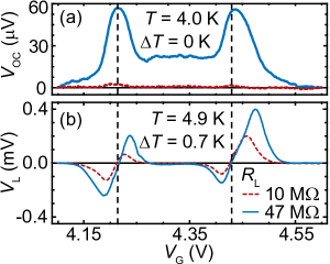
In order to measure, , the parasitic is reduced by adding an external load resistance, , to the system (see Fig. 1b). Current flows to ground through and dissipates , but unfortunately also dissipates . Specifically, when is finite, current flows through the system, and the preamp measures the induced voltage across the load resistor. because is (by definition) the thermally induced voltage at zero current. Simple circuit analysis reveals that (dc) , where is a function of as given by the nanowire conductance, . Therefore, when choosing , a tradeoff must be made between decreasing while maintaining . We have best results when is between the on- and off-resonance values of , that is, when . As shown in Fig. 3, at K when M, and in comparison, this is roughly twice as large as its M version at finite .
This research was supported by The Nanometer Structure Consortium at Lund University, ONR, Energimyndigheten, the Foundation for Strategic Research (SSF), the Knut and Alice Wallenberg Foundation, and an NSF-IGERT Fellowship.
References
- Hochbaum, et al. (2008) A. I. Hochbaum, et al., Nature 451, 163 (2008).
- Boukai, et al. (2008) A. I. Boukai, et al., Nature 451, 168 (2008).
- Chickering, et al. (2009) W. E. Chickering, et al., Phys. Rev. Lett. 103, 046807 (2009).
- Humphrey, et al. (2002) T. E. Humphrey, et al., Phys. Rev. Lett. 89, 116801 (2002).
- Kim, et al. (2009) R. Kim, et al., J. Appl. Phys. 105, 034506 (2009).
- Hoffmann, et al. (2009) E. A. Hoffmann, et al., Nano Lett. 9, 779 (2009).
- Hoffmann and Linke (2009) E. A. Hoffmann, and H. Linke, Journal of Low Temperature Physics 154, 161 (2009).
- van Houten, et al. (1992) H. van Houten, et al., “Coulomb-blockade Oscillations in Semiconductor Nanostructures,” in Single Charge Tunneling, edited by H. Grabert, and M. Devoret, Plenum, New York, 1992, vol. B294 of NATO ASI, (see also e-print http://arxiv.org/abs/cond-mat/0508454).