Single-electron turnstile pumping with high frequencies
Abstract
In this Letter, we present a theoretical analysis to single-electron pumping operation in a large range of driving frequencies through the time-dependent tunneling barriers controlled by external gate voltages. We show that the single-electron turnstile works at the frequency lower than the characteristic frequency which is determined by the mean average electron tunneling rate. When the driving frequency is greater than the characteristic frequency of electron tunnelings, fractional electron pumping occurs as an effect of quantum coherence tunneling.
pacs:
85.35.Gv, 73.63.-b, 03.65.YzSingle-electron pumps and turnstiles are nanoscale tunneling devices utilizing controllable transfer of electrons one-by-one synchronized with alternating external gate voltages. These devices are supposed to have important applications as current standards and also as high-frequency amplifiers/detectors in solid-state quantum computing. Electrons pumping operations have been experimentally demonstrated with various nanoscale tunneling structures, in particular, through switching-on and off the tunneling barriers setp1 ; set4 ; set5 ; set6 ; pumps . These experimental realizations for single-electron turnstiles are basically operated at relatively low frequencies ( hundreds MHz to a few GHz) with a small pumped current ( tens to hundreds pA). To understand the single-electron pumping mechanism at higher frequencies with a larger pumping current, we shall closely monitor the electron transfer in these nanoelectronic devices with a large range of the signal frequencies. We shall utilize the exact nonequilibrium quantum transport theory for nanodevices we developed recently Jin10083013 and focus on the single-electron device with time-dependent tunneling barriers controlled by external gate voltages, to examine the real-time dynamics of the electron transfer far away from equilibrium.
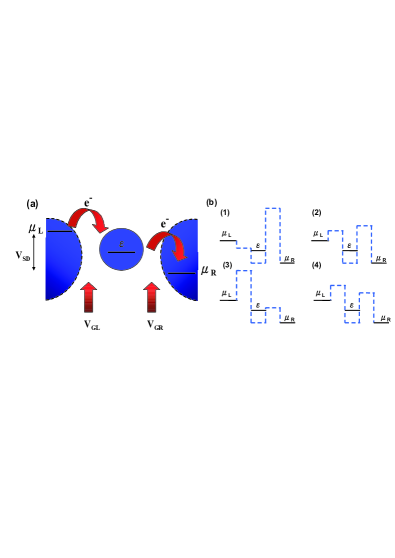
We model the single-electron device by a quantum dot junction of a single level quantum dot coupling to a source and a drain, as schematically shown in Fig. 1(a). The pump or turnstile operations are realized by imposing the repetitive pulses to tune the tunneling barriers. As the gate voltages and are applied to gate, the tunneling barriers vary in time. By modulating the tunnel barriers, it has been observed setp1 ; set4 ; set5 ; set6 ; pumps that electrons can be transferred one-by-one between the source and the drain. Here we follow the experimental setup given in Ref. setp1 where the barriers are modulated in anti-phase and the dot level is kept fixed. Fig. 1(b) plots schematically the barrier changing process from (a) to (d) and then repeat continually in time. Also, a dc bias voltage is applied between the source and drain to examine the single-electron pumping dynamics in a large range of driving frequency.
Based on the recently developed non-equilibrium quantum transport theory Jin10083013 which is derived from the exact master equation for nanoelectronics Tu08235311 , the transient electron occupation number in the dot and the transient electron current flowing from the leads into the dot are given by
| (1a) | |||
| (1b) | |||
respectively, where denote the left and right leads (source and drain). The functions and in Eq. (1) are related to the retarded and correlation Green functions that satisfy the dissipation-fluctuation integrodifferential equations of motion Tu08235311 ; Jin10083013 :
| (2a) | |||
| (2b) | |||
with the initial condition . in Eq. (1) is the initial electron occupation in the dot. Here, the non-local time-correlation functions and with
| (3a) | ||||
| (3b) | ||||
in which are the initial electron distribution functions in the leads at the initial temperature , and the corresponding chemical potentials. are the spectral densities with being the densities of states of the leads, and the lead-dot coupling coefficients. The integration in Eq. (2) with the kernels and encompass all the back-reaction non-Markovian memory effects between the leads and dot associating with quantum dissipation and fluctuation. These effects must be fully taken into account for the accuracy of transient electron transfer.
In reality, the spectral densities have more or less a Lorentzian-type shape Mac06085324 ; Tu08235311 ; Jin10083013 ,
| (4) |
where are the time-dependent electron tunneling rate from the leads to the dot that can be controlled by the gate voltages , and are the bandwidths of the spectral densities. The explicit relation between the tunneling rate and the gate voltage can be obtained by solving the Schrödinger equation of a one-dimensional scattering problem,
| (5) |
with = and =, where is the width of barrier, and the effective mass of the electron in the sample. To study electron pumping processes, we apply a square wave modulation and a sinusoidal wave modulation to vary the tunneling barriers between the leads and the dot. For the square wave, and vary from to in frequency with a phase shift. For the sinusoidal wave, , and . Fig. 2(a)-(b) plot the corresponding tunneling rate .

To monitor the single electron pumping dynamics, a dc bias voltage is also applied to the leads. The initial temperature of the leads is taken at . We also fix the bandwidth of the spectral density by which is close to the wide band limit. If we take =0.1 meV, the corresponding temperature is about mK. We may also take the on-site-energy of the dot and the applied bias voltage at the same scale, e.g. =1 meV and =2 meV. All these parameters are controllable in experiments. To investigate the turnstile operation at different driving frequency regime, we vary the driving field from the low to high frequencies. The low and high frequency regimes are divided with respect to the electron response time which is determined by the so-called dwell timeButtiker96 ; Guo07 . The dwell time, defined by =4/, is a time scale characterizing the time of the electron relaxing out the dot. For the above setup of the system, taking an mean value average tunneling rate in each cycle, we obtain =26.3 ps for square wave modulation and 63.12 ps for sinusoidal wave modulation, which correspond to the characteristic frequencies GHz and 15.8 GHz, respectively.
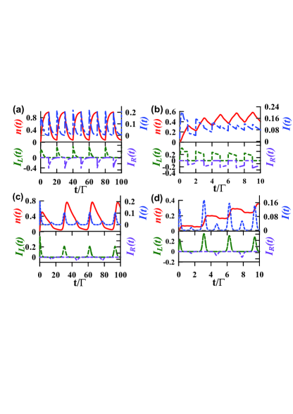
Now, we discuss how the electron turnstile operates under time-dependent tunneling barriers. In Fig. 3(a)-(b), we plot the time-dependent electron population in the dot, the left and right current flowing into the dot, given by Eq. (1), as well as the pumping current under the control of a square wave gate voltage. When the left barrier is opened to the source gate and the right barrier is closed, the electron tunnels from the source to the dot in each cycle with an increasing electron population and a positive current, as shown in Fig. 3(a). When the left barrier is closed and the right barrier is opened, the electron tunnels from the dot to the drain with a decreasing population and a negative current. However, the device operated under different driving frequency behaves significantly different. When the device is operated with a low driving frequency: , the electron tunnels from the source to the drain one-by-one in each cycle. Fig. 3(a) shows that the electron population changes roughly between zero to one in each cycle. The corresponding time-dependent left and right currents flowing into the dot also clearly show that the electron transfer is dominated by sequential tunnelings. However, with the higher driving frequency, , the electron population varies from 0.4 to 0.6 in each cycle, as shown in Fig. 3(b). In other words, the driving field oscillates faster than the response of the electron tunneling such that the electron only partially tunnels into the dot in each cycle.
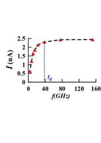
To have a clear picture how the single-electron turnstile operates at high frequencies, we plot in Fig. 4 the pumping current as a function of driving frequency for the square wave modulation. It shows that when , the pumping current (for ). This substantiates the electron transfer one-by-one synchronized with alternating external gate voltages, as observed in Ref. setp1 as well as in other experimental setup set4 ; set5 ; set6 ; pumps . However, for the operating frequency , the electron transfer deviates gradually from the above linear relation. When , the pumping current is saturated and becomes a constant. As a result, the electron turnstile operation, namely, the electron transfer one-by-one synchronized with alternating external gate voltages obeying the relation works well when .
Same plot is given for the sinusoidal wave modulation, see Fig. 3(c)-(d). Different to the square wave modulation, sinusoidal wave only has a very short period of time that can totally open the tunneling channels for the source and the drain, as shown by the time-dependence of in Fig. 2(b). This makes the electron never have a sufficient time to fully tunnel into the dot even when the device operates at a low frequency, , see the plot in Fig. 3(c) where the maximum occupation is about 0.8. Moreover, the average tunneling rate of the sinusoidal wave modulation is smaller than that in the square wave modulation for each cycle. Correspondingly the electron dwell time becomes longer for the sinusoidal wave modulation. As a result, with a high driving frequency, , only a fraction of the electron charge can be tunneled into the dot in every cycle until the system reaches its steady state, as shown in Fig. 3(d). This is indeed a quantum coherence tunneling, namely the tunneling electron is in a superposition state between the lead and the dot.
To make this phenomenon clearer, we may only turn on the left tunneling (between the source and the dot) but close the right tunneling (between the dot and the drain). The corresponding results are plotted in Fig. 5(a) where the driving frequency, =50 GHz, is greater than . As we can see, in each cycle the electron transfer shows a plateau of fractional charge. In other words, in the high driving frequency regime, only fractional electron rather than the single electron is pumped in each cycle. The same phenomenon is also seen under a different setup, namely closing the left tunneling but turning on the right tunneling channel with the initial occupation , the result is shown in Fig. 5(b).

In conclusion, our analysis on the transient electron transport show that the external driving field under different driving frequency regimes manipulates quite different electron pumping dynamics. When the external driving frequency is lower than the characteristic frequency (proportional to the mean average electron tunneling rate through the dwell time ), the single-electron turnstile pumping, namely the controllable transfer of electrons one-by-one synchronized with alternating external gate voltages, works well, as observed in experiments. Operating the turnstile device at high frequency with a large pumping current requires an increase of the effective tunneling rate (shortening the electron response time) between the central system with its contacts, which is controllable by the gate voltage profile of the external driving field. As we have shown, the square wave modulation has a larger than the sinusoidal wave modulation so that it can operate the single-electron turnstile with a higher signal frequency for the same driving field strength. However, the sinusoidal wave modulation in the high frequency regime leads to the fractional electron pumping, as a new quantized electron transfer phenomenon. Such fractional electron pumping phenomenon should be observed in experiments with the current advances in the nanofabrication technology, and may also have the potential application in precision measurement as well as in solid-state quantum computing.
This work is supported by the National Science Council of ROC under Contract No. NSC-99-2112-M-006-008-MY3 and National Center for Theoretical Science.
References
- (1) L. P. Kouwenhoven, A. T.Johnson, N. C. van der Vaart, C. J. P. M. Harmans, and C. T. Foxon, Phys. Rev. Lett. 67, 1626 (1991).
- (2) A. Fujiwara, N. M. Zimmerman, Y. Ono, and Y. Takahashi, Appl. Phys. Lett. 84, 1323 (2004); A. Fujiwara, K. Nishiguchi and Y. Ono, Appl. Phys. Lett. 92 042102 (2008).
- (3) M. D. Blumenthal, B. Kaestner, L. Li, S. Giblin, T. J. B. M. Janssen, M. Pepper, D. Anderson, G. Jones and D. A. Ritchie, Nat. Phys. 3, 343 (2007).
- (4) J. P. Pekola, J. J. Vartiainen, M. Möttönen, O.-P. Saira, M. Meschke, and D. V. Averin, Nat. Phys. 4, 120 (2008).
- (5) S. P. Giblin, S. J. Wright, J. D. Fletcher, M. Kataoka, M. Pepper, T. J. B. M. Janssen, D. A. Ritchie, C. A. Nicoll, D. Anderson, and G. A. C. Jones, New J. Phys. 12, 073013 (2010).
- (6) J. S. Jin, M. W. Y. Tu, W. M. Zhang, Y. J. Yan, New J. Phys. 12, 083013 (2010).
- (7) M. W. Y. Tu and W. M. Zhang, Phys. Rev. B 78, 235311 (2008).
- (8) J. Maciejko, J. Wang, and H. Guo, Phys. Rev. B 74, 085324 (2006).
- (9) V. Gasparian, T. Christen, and M. Büttiker, Phys. Rev. A 54, 4022 (1996).
- (10) J. Wang, B. Wang, and H. Guo, Phys. Rev. B 75, 155336 (2007).