Plasmon and coupled plasmon-phonon modes in graphene
Abstract
Plasmon and coupled plasmon-phonon modes in graphene are investigated theoretically within the diagrammatic self-consistent field theory. It shows that two plasmon modes and four coupled plasmon-phonon modes can be excited via intra- and inter-band transition channels. It is found that with increasing and carrier density, the plasmon modes couple strongly with the optic-phonon modes in graphene. The coupled plasmon-phonon modes exhibit some interesting features which can be utilized to realize the plasmonic devices. Our results suggest that the carrier-phonon interaction should be considered to understand and explain the properties of elementary electronic excitations in graphene.
pacs:
73.20.Mf, 72.10.Di, 81.05.ueI Introduction
Since graphene was discovered in 2004 ksn , it has brought us many surprises and opened up a new field of research in condensed matter physics and nano-electronics. From a physics point of view, carriers in graphene are massless, gapless and relativistic Dirac particles with nearly linear energy dispersion. Thus graphene brings us a great opportunity to look into the many-body interactions in a Dirac quasi-particle system. Recently the elementary electronic excitation via plasmon modes resulting from Coulomb interaction has been intensively investigated for graphene based electronic systems. Das Sarma and Hwang das and Wang and Chakraborty wxf have found theoretically that the plasmon frequency of the Dirac fermions in graphene shows very different behaviors from the usual 2DEG systems. More interestingly, it has been shown that the plasmon frequencies in graphene can be within the terahertz ( Hz or THz) bandwidth vra and 1 - 10 THz sources based on plasmon amplification in graphene can be generated for moderate carrier densities by applying the gate voltages fr . Moreover, Jablan et.al. has demonstrated that the plasmon excitation in graphene can have low losses for infrared frequencies jabl and proposed that such a feature can be utilized for nano-photonic device applications. The results obtained from further theoretical investigations have indicated that the guided plasmon waves in graphene p-n junctions can be achieved and graphene can then be applied as a material for nano-plasmonics egm . However, here we notice that most of the published theoretical studies mentioned above were carried out without considering the carrier-phonon coupling in graphene and only the intra-band transition channel was taken into consideration. Very recently, Bostwick et.al. observed the plasmarons in free-standing doped graphene, which results from bound states of charge carriers with plasmons plaron .
On the other hand, recent experimental work has suggested that the adiabatic Born-Oppenheimer approximation fails in graphene because of the presence of the interactions between the peculiar Dirac fermions and optic phonons pisa . It has been experimentally demonstrated that the plasmon modes in epitaxial graphene on SiC wafer can be strongly coupled with the surface optical phonon modes in silicon carbide liuy . Bostwick et.al. have found experimentally that the electron-electron interaction and the electron-phonon coupling should be considered on an equal footing to understand the properties of Dirac quasi-particles in graphene bos . Siegel et.al. have experimentally demonstrated electron-electron interaction results in unique renormalizations, electron-phonon interaction diminish with decreasing doping in graphene pnas . The measurement of the Raman spectrum has now been widely used to investigate the properties of photo-excited electronic excitations in graphene systems cst ; dmb . The results obtained from recent Raman measurements have shown that the position of optic-phononinduced G-peak depends very weakly on carrier density in the sample. However, the Raman intensity around the G-peak increases with increasing doping concentration in graphene. Such an effect is an identification that both the electron-electron interaction and the electron-phonon coupling affect strongly the elementary electronic excitations in graphene. These experimental findings have clearly indicated that the carrier-phonon coupling is very important in understanding and explaining the electronic and optoelectronic properties of graphene, especially the elementary electronic excitations.
We know that in conventional electronic gas systems the plasmon modes can be strongly modified by phonon scattering so that the new modes, namely the coupled plasmon-phonon modes, are formed. Raman scattering moo , infrared and photoemission measurements tak , and ultrafast pump-and-probe experiments alt , etc. have been widely applied to detect and study the coupled plasmon-phonon modes in semiconductor based bulk and low-dimensional electronic systems. The investigation of the plasmon and coupled plasmon-phonon excitations from electron gas systems is also a fundamental basis for the realization of these systems as plasmonic devices for various applications. Because graphene is an ideal 2DEG system with high carrier density and high carrier mobility, it is natural for us to expect that graphene can exhibit more excellent and unique plasmonic properties for device applications. Thus, in order to gain an in-depth understanding of the many-body interactions in graphene systems and, on this basis, to explore the potential applications of graphene as practical nano-plasmonic devices, it is necessary and significant to examine the roles which the carrier-carrier interaction and the carrier-phonon coupling can play in such a Dirac fermion system. And this becomes the prime motivation of the present theoretical investigation.
II Theoretical approach
Here we consider a graphene sheet in the -plane. A carrier (electron or hole) in a monolayer graphene can be described by the Dirac equation for a massless neutrino. The energy spectrum and wavefunction for a Dirac quasi-particle in graphene in the absence of the scattering mechanisms can be obtained analytically. They are, respectively, and in the form of a row matrix. Here, is the wavevector for a carrier and , , is the band parameter with cm/s being the Fermi-velocity of a Dirac quasi-particle, for an electron and for a hole, and is the angle between and the direction.
With the single-particle wavefunction for a carrier, we can calculate the electrostatic energy induced by bare carrier-carrier (c-c) interaction in graphene through
where is the Coulomb potential with being the high-frequency dielectric constant for graphene layer wxf , and or is a sign function related to the charge sign of a carrier in different bands. After considering a momentum conservation law, namely the momentum that flows into the c-c scattering conserves with what flows out for different scattering processes, the bare c-c interaction becomes
| (2) |
where we have defined for intra- (i.e., ) and inter-band (i.e., ) transition, is the change of the carrier wavevector during a c-c scattering event, is the two-dimensional Fourier transform of the Coulomb potentail, and
with , and being the angle between and .
In the present study, we assume that the graphene system can be separated into the carriers of interest and the rest of graphene crystal. For the case of carrier interactions with 2D-like phonons, the interaction Hamiltonian takes a form
| (3) |
where is the phonon wavevector along the xy-plane, are the canonical conjugate coordinates of the phonon system, is the carrier-phonon (c-p) interaction coefficient, and is the phonon frequency. The Fourier transform of the matrix element for bare c-p interaction can be written as
| (4) |
where is the electronic excitation frequency, is the bare phonon propagator, and . The published experimental results have indicated that the optic-phonon coupling is a major factor in determining the intensity and peak-position of phonon-related Raman spectrum in graphene cst ; dmb . Thus, in conjunction with these experimental findings, in this study we consider carrier interaction with only optic-phonons. On the basis of a valence-force-field model, the coupling coefficient for carrier interactions with long-wavelength optic-phonons in graphene is tse
| (5) |
where with g/cm2 being the areal density of the graphene sheet, meV the optic-phonon frequency at the -point, is a dimensionless parameter, and is the equilibrium bond length. Furthermore,
| (6) |
for coupling with, respectively, the longitudinal () and transverse () phonon modes, where is the angle between and the x-axis. Thus, the squares of the carrier-phonon scattering matrix elements are
and
The total contribution of the optic-phonon scattering is
| (7) |
which is independent on and . This feature is very distinct from that in the conventional semiconductor-based 2DEG systems.
In a diagrammatic self-consistent field theory wxu , the effective c-c interaction in the presence of the c-p coupling is given by
where is the dynamical dielectric function matrix element and
is the pair bubble or density-density correlation function in the absence of the c-c screening, with being the Fermi-Dirac function for a carrier in the band and and counting respectively the spin and valley degeneracy. After summing over and setting and , the dielectric function matrix is obtained as
| (8) |
where
is induced by the c-c interaction, and
is caused by the c-p coupling. In this study we use a matrix to present the dielectric function. In contrast to previous theoretical study in which only the intra-band transition is considered for calculating the dynamical dielectric function, the present work includes the contributions from inter-band transition channels as well. Thus, the dielectric function matrix is a matrix. In the absence of the phonon scattering, i.e., when , the dynamical dielectric function matrix becomes that obtained under the standard random phase approximation (RPA). The determinant of the dielectric function matrix Eq. (II) is given by
| (9) |
which results from intra- (i.e., or ) and inter-band (i.e., or ) electronic transitions. The modes of the elementary electronic excitation are determined by .
Now we consider a n-type (or positively gated) graphene with an electron density and a distribution function where is the Fermi energy (or chemical potential) for electrons in the conduction band. In such a case, the valence band is fully occupied so that the distribution , the hole density , and . The approach can also be applied to the p-type (or negatively gated) graphene samples because the electrons and holes are symmetrical in graphene system. At a long-wavelength () and low-temperature () limit, the frequency of the collective excitation of the uncoupled plasmon mode () is obtained as
| (10) |
which is induced by intra-band transition within the conduction band. Here, kF with kF being the Fermi wavevector in graphene and q is defined as the plasmon wavevector or momentum. By solving the equation
| (11) |
we can obtain the uncoupled plasmon mode induced by inter-band transition for electrons from valence band to conduction band in graphene. Similar to a conventional 2DEG system, the single-particle (electron-hole pair) excitations (SPE) for intra- and inter-band transition channels are also allowed in graphene. The intra- (upper) and inter- (lower) band transition boundaries are still given respectively by . Thus, we are able to identify the intra-band SPE regime for kF, and for kF. The inter-band SPE regime is allowed for in graphene. Furthermore, a critical parameter kF can be introduced to indicate the minimum momentum transfer with , where the plasmon mode enters to the electron-hole continuum.
Including the electron-phonon coupling , we obtain two coupled plasmon-phonon modes,
| (12) |
induced by intra-band transition for electrons within the conduction band in graphene, where . Moreover, by solving the equation
| (13) |
we acquire two coupled plasmon-phonon modes and induced via inter-band transition for electrons from valence band to conduction band in graphene system. The analytical results presented in this Section show that after including the inter-band transition channels and the electron-phonon coupling, the new modes of elementary electronic excitations can be achieved in graphene.
III Numerical results and discussions
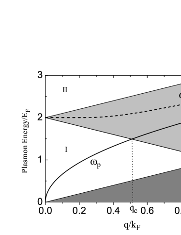


In Fig. 1, the dispersion relation for uncoupled plasmon modes, and induced respectively by intra- and inter-band transitions, are shown at a fixed electron density in graphene. As being pointed out by other authors das ; wxf , the plasmon frequency induced by intra-band excitation in graphene, , is acoustic-like and depends strongly on q. The density dependence in graphene differs from that in a conventional 2DEG system. It shows that the plasmon frequency of graphene can be effectively controlled through tuning carrier densities by gated voltages. In the presence of the inter-band transition channels, we obtain a new uncoupled plasmon mode induced by excitation of electrons from occupied valance band to the empty states in the conduction band. Due to Pauli exclusion principle, is optic-like and depends relatively weakly on q. With increasing q, and converge in regime III. We find that depends more strongly on carrier density and q than does. For a undoped graphene sample so that , the plasmon frequency and the excitation is restricted, whereas there exits the plasmon mode with a frequency due to inter-band electronic transition. Thus, this new plasmon mode can be used to investigate the collective electronic excitation from an nearly intrinsic graphene. In Fig. 1, we also show the regimes III and IV for kF within which the SPE can take place. Similar to a conventional 2DEG, within the SPE regime the Landau damping occurs so that the imaginary part of the dielectric function Im, and that if the plasmon excitation exists in these regimes for kF (see e.g. III and IV in Fig. 1), the plasmon modes are strongly damped and decay into the electron-hole pairs. Thus, one can see that the plasmon mode is undamped for in regime I where Im, whereas the plasmon mode is damped in the full regime of III in which Im. Consequently, in graphene, the undamped plasmon excitation can be achieved via intra-band transition, while the plasmon excitation via inter-band transition is damped due to the Landau damping effect.
In Fig. 2, the dispersion relation for coupled plasmon-phonon modes and induced by intra-band transition is shown for different electron densities. For small values of , the lower frequency branch is acoustic-like (or plasmon-like) which depends strongly on q, whereas the higher frequency branch is optic-like (or phonon-like) which depends rather weakly on q. Interestingly, for relatively large values of , the lower frequency branch becomes optic-like and , whereas the higher frequency branch is acoustic-like and . When , the plasmon modes couples strongly to the optic-phonon modes and the frequencies of the coupled plasmon-phonon modes in graphene differ significantly from the corresponding plasmon and optic-phonon frequencies. The value, at where the two branches of the excitations change the nature of the q dependence, decreases with increasing the electron density. It is interesting to compare the results for the coupled plasmon-phonon modes in graphene with those in a conventional 2DEG (C2DEG) system. In a semiconductor based C2DEG, there exit three modes for coupled plasmon-phonon excitations induced by intra-subband transition channels via electron interaction with optic-phonons through Fröhlich coupling pee . They are: i) longitudinal-optic (LO) phonon-like mode with being the LO-phonon frequency; ii) transverse-optic (TO) phonon-like mode with being the TO-phonon frequency; and iii) plasmon-like mode , respectively. In a C2DEG, the plasmon-like mode does not coupled markedly with the phonon-like modes and the phonon-like modes depend quite weakly on q pee . The reason why only two coupled plasmon-phonon modes are observed in graphene is that at the -point, for graphene tse in contrast to a C2DEG where normally at the -point. The different q-dependence of the coupled plasmon-phonon modes in graphene and in a C2DEG is mainly induced by different energy spectra in two electronic systems. As we know, the elementary electronic excitation is achieved via varying the energy and momentum of the electrons. Thus, the energy spectrum of the electronic system determines mainly the dispersion relation of the electronic excitation. In contrast to a parabolic energy spectrum for a C2DEG, graphene has a linear energy spectrum. As a result, the dispersion relation of the coupled plasmon-phonon modes in graphene differs significantly from those in a C2DEG. From Fig. 2, we can also find that with increasing electron density , the value decreases, and the plasmon and phonon modes are strongly coupled. This is because the plasmon frequency in graphene can be comparable to the optic-phonon frequency at a relatively large .
In Fig. 3, we show the dispersion relation for coupled plasmon-phonon modes with frequencies and induced by inter-band transition in graphene for different electron densities . We see that a strong optic-phononlike mode with a frequency can be generated in graphene and the frequency of this mode depends very weakly on both q and the electron density. In contrast, the plasmon-like mode depends sensitively on electron density and on plasmon wavevector q. increases with due to its plasmon-like nature of the excitation. We note that both modes with and are optic-like and uncoupled with each other. For a n-type graphene, an excitation energy is required to excite electrons in the valence band into the conduction band and to induce the elementary electronic excitations due to the phase-space restriction. As a result, there are always and for coupled plasmon-phonon frequencies induced by inter-band transition in graphene and these modes are undamped by the Landau-damping effect.
It is known that the elementary electronic excitation can be achieved in an electron gas system through electronic transition from occupied lower-energy states to the empty higher-energy states. This includes both intra- and inter-band excitations. In a semiconductor based C2DEG, because the band-gap between the conduction band and the valence band is quite large, the inter-band electronic transition requires a quite large excitation energy and thus is less possible. However, graphene is a gapless 2DEG and the inter-band electronic transition in graphene can therefore be achieved via a small energy transfer. Hence, the elementary electronic excitation via plasmon and coupled plasmon-phonon modes induced by inter-band transition can be more possibly achieved in graphene than in a C2DEG. Because the carrier density in graphene can be effectively modulated up to cm-2 by applying the gate voltages jabl ; liuy ; bos , the plasmon and coupled plasmon-phonon excitations can be experimentally detected and studied by different methods liuy ; alt . It is found experimentally that the position of the G-peak induced by optic-phonon scattering in the Raman spectrum in graphene varies very little with varying the carrier density in the sample. However, the Raman intensity around the G-peak depends quite strongly on the carrier density in graphene. The results from the present study show that for small values of , optic-phononlike modes can be generated through coupled plasmon-phonon excitations via intra-band (see in Fig. 2 for ) and inter-band (see in Fig. 3) electronic transition channels. Such modes depend rather weakly on and for small values of . This suggests that the position the optic-phononinduced G-peak in the Raman spectrum does not change significantly with varying the carrier density in the sample, in line with the experimental finding. From Fig. 2, we see that for relatively large values of which decreases with increasing , the frequency of optic-phononlike mode induced by intra-band excitation depends strongly on electron density. This implies that the Raman intensity around the G-peak can be altered with varying the carrier density in graphene. Because the optic-phononlike mode induced by inter-band excitation depends very little on (see Fig. 3), the change of the Raman intensity around the G-peak is mainly induced by intra-band excitation mechanism. Thus, our results can be applied to understand and explain the experimental findings. These experimental and theoretical results indicate that the electron-phonon interaction can affect strongly the features of elementary electronic excitations in graphene. Furthermore, the results shown in Figs. 2 and 3 demonstrate that the coupled plasmon-phonon excitations in graphene can provide frequency-tunable plasmonic modes. Hence, graphene can be used as plasmonic device for various applications.
IV Conclusions
In this work, we have developed a tractable theory approach to study the plasmon and coupled plasmon-phonon modes in graphene in which the carrier-carrier interaction and the carrier-phonon coupling are taken into consideration. We have also included the effect of the presence of the inter-band electronic transition channels within our calculations. The main conclusions obtained from this study are summarized as follows.
An acoustic-like plasmon mode with a frequency can be generated via intra-band electronic transition in graphene and the carrier density dependence of this mode differs from that in a conventional 2DEG. This is in line with previous theoretical finding. We have found that an optical-like plasmon mode with a frequency can be excited via inter-band electronic transition in graphene. However, this mode is within the Landau-damping regime.
We have found that four coupled plasmon-phonon modes can be generated in graphene. The features of two coupled-phonon modes induced by intra-band transition channels differ significantly from those observed in a conventional 2DEG system. Two optic-like modes for coupled plasmon-phonon excitation can be observed via inter-band electronic transition channels. Three coupled plasmon-phonon modes depends strongly on electron density and plasmon wavevector.
The results obtained from this study demonstrate that if the inter-band transition channels are taken into consideration, new modes for plasmon and coupled plasmon-phonon excitations can be obtained in graphene. The properties of the plasmon and coupled plasmon-phonon excitations in graphene are very distinct from those in the conventional 2DEG systems. Our results confirm that the carrier-carrier interaction and the carrier-phonon coupling should be equally considered to understand the properties of elementary electronic excitation in graphene. Finally, our results presented and discussed in this paper can be used to understand and explain the experimental findings obtained from, e.g., the Raman measurements.
Acknowledgements.
Academy of Sciences, National Natural Science Foundation of China and Department of Science and Technology of Yunnan Province, China. One of us (H.M. Dong) was supported by Max Planck Society/Chinese Academy of Sciences Doctoral Promotion Program.References
- (1) K.S. Novoselov, A.K. Geim, S.V. Morozov, D. Jiang, Y. Zhang, S.V. Dubonos, I.V. Grigoreva, and A.A. Firsov, Science 306 (2004) 666.
- (2) S. Das Sarma and E.H. Hwang, Phys. Rev. Lett. 102 (2009) 206412.
- (3) X.F. Wang and T. Chakraborty, Phys. Rev. B 75 (2007) 033408.
- (4) V. Ryzhii, A. Satou, and T. Otsuji, J. Appl. Phys. 101 (2007) 024509.
- (5) F. Rana, IEEE Transactions on Nanotechnology 7 (2008) 91.
- (6) M. Jablan, H. Buljan, and Soljai, Phys. Rev. B 80 (2009) 245435.
- (7) E.G. Mishchenko, A.V. Shytov, and P.G. Silvestrov, Phys. Rev. Lett. 104 (2010) 156806.
- (8) A. Bostwick, F. Speck, T. Seyller, K. Horn, M. Polini, R. Asgari, A.H. MacDonald and E. Rotenberg, Science 328 (2010) 999.
- (9) S. Pisans, M. Lazzeri, C. Casiraghi, K.S. Novoselov, A.K. Geim, A.C. Ferrari and F. Mauri, Nature Materials 6 (2007) 198.
- (10) Y. Liu and R.F. Willis, Phys. Rev. B 81 (2010) 081406(R).
- (11) A. Bostwick, T. Ohta, T. Seyller, K. Horn, E. Rotenberg, Nat. Phys. 3 (2007) 36.
- (12) D.A. Siegel, Cheol-Hwan Park, C.Y. Hwang, Jack Deslippe, A.V. Fedorov, S.G. Louie and A. Lanzara, PNAS 108 (2011) 11365.
- (13) C. Stampfer, F. Molitor, D. Graf, K. Ensslin, A. Jungen, C. Hierold and L. Wirtz, Appl. Phys. Lett. 91 (2007) 241907.
- (14) D. M. Basko, S. Piscanec, and A. C. Ferrari, Phys. Rev. B 80 (2009) 165413.
- (15) A. Mooradian and G.B. Wright, Phys. Rev. Lett. 16 (1966) 999.
- (16) T. Iwanaga, T. Suzuki, S. Yagi and T. Motooka, Appl. Phys. Lett. 86 (2005) 263102.
- (17) G.C. Cho, T. Dekorsy, H.J. Bakker, R. Hvl, and H. Kurz, Phys. Rev. Lett. 77 (1996) 4062; H. Altan, X. Xin, D. Matten, and R.R. Alfano, Appl. Phys. Lett. 89 (2006) 052110.
- (18) W.K. Tse and S. Das Sarma, Phys. Rev. Lett. 99 (2007) 236802; T. Ando, J. Phys. Soc. Jpn. 76 (2007) 024712.
- (19) W. Xu, M.P. Das and L.B. Lin, J. Phys.: Condens. Matter 15 (2003) 3249.
- (20) X.G. Wu, F.M. Peeters, J.T. Devreese, Phys. Rev. B 32 (1985) 6982(R).