Conductance fluctuations in graphene devices with superconducting contacts in different charge density regimes
Abstract
Conductions fluctuations (CF) are studied in single layer graphene devices with superconducting source and drain contacts made from aluminium. The CF are found to be enhanced by superconductivity by a factor of 1.4 to 2. This (near) doubling of the CF indicates that the phase coherence length is . As compared to previous work, we find a relatively weak dependence of the CF on the gate voltage, and hence on the carrier density. We also demonstrate that whether the CF are larger or smaller at the charge neutrality point can be strongly dependent on the series resistance , which needs to be subtracted.
I Introduction
Graphene has proven to be interesting for the study of conductance fluctuations (CF) in disordered systems Morozov et al. (2006); Heersche et al. (2007); Ojeda-Aristizabal et al. (2009); Skákalová et al. (2009); Trbovic et al. (2010). Some of its remarkable properties are the linear low energy band structure Geim and Novoselov (2007) and the K-K’ degeneracy, which leads to unusual scattering McCann et al. (2006). In common supported graphene devices disorder is inevitably introduced by the substrate and CF have been shown to be major corrections to the transport at low temperature.
In numerical calculations Rycerz et al. (2007); Borunda et al. (2011) stronger CF were found away from the charge neutrality point (CNP). Additionally, the CF were reported to be non-ergodic and they were suspected to result from variations in trajectories, rather than in phase shifts Rycerz et al. (2007). The results and interpretation of Rycerz et al. (2007) were debated in Kharitonov and Efetov (2008), where CF were studied analytically and a similar magnitude of the CF was found but with fulfilled ergodicity.
Superconducting electrodes can provide additional information on the transport mechanisms in disordered systems Beenakker (1995). Phase sensitive Andreev reflection can occur at the interface between the superconductor (S) and the normal conducting graphene (G). At energies below the superconducting gap electrons from G can only enter S in the form of a Cooper pair. This charge transfer needs time reversal symmetry, which can be broken by the application of an external magnetic field.
In the following, we look at CF in a two-terminal graphene device with superconducting contacts. We compare the CF in the superconducting and normal state of the electrodes. The latter is achieved by either increasing the temperature or by applying a magnetic field. The CF near and far away from the CNP are presented.
II Sample preparation and experimental set-up
Mechanical Microcleavage Novoselov et al. (2005) was used to deposit the graphene flakes onto a highly p-doped silicon wafer, covered by 300 nm silicon dioxide. The silicon wafer serves as a back-gate where a voltage is applied.
The graphene flakes on the substrate were located with optical microscopy and categorised by optical contrast. To ensure that the selected flakes are indeed single layer graphene, Raman spectroscopy Ferrari et al. (2006) with 532 nm laser light was performed.
Subsequently, a PMMA mask was used to pattern the electrical lines by electron beam lithography. A thin metal film (5 nm Ti / 50 nm Al) was evaporated on the sample in a UHV e-gun evaporation system. After lifting the PMMA mask off, the sample was cleaned in chemical solvents (acetone, ethanol and 2-propanol) and annealed in vacuum at 200 ∘C for several hours.
The inset of figure 1 shows a micrograph of the device investigated. The single layer graphene flake is approximately of length 1.3 m and width 3.8 m.
Electrical measurements were performed in an Oxford Instruments 3He cryostat at temperatures in the range of 230 mK - 1.5 K. A Stanford Research Systems SR830 lock-in amplifier was used to apply a 20 V AC voltage which was superimposed onto a DC voltage . The current through the sample was detected by an IV converter. No series resistors (like the electrical lines of the cryostat or the impedance of the IV converter) were subtracted from the data, unless mentioned.
III Results and discussion
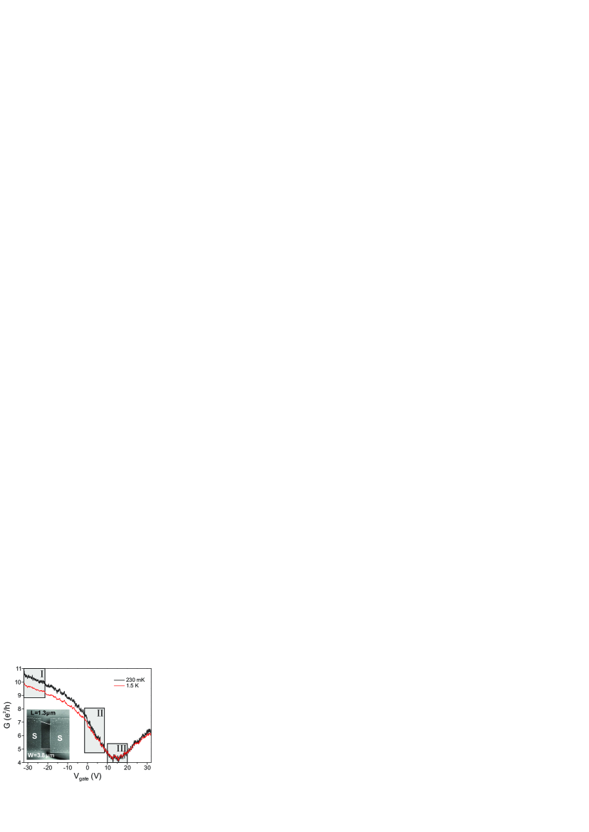
Figure 1 shows the measured two-terminal conductance through the device as a function of the back-gate voltage , for two different temperatures, 230 mK and 1.5 K. At low temperature, the Al contacts are in the superconducting state, while for the higher temperature they are normal. The charge neutrality point (CNP), indicated by the minimum in , lies at 15 V which suggests p-doping. Charged impurities introduce scattering and thus disorder Chen et al. (2008) which is responsible for the broad shape of the dip in .
At large doping, i.e. for small negative gate voltages, the conductance is reduced in the normal state by 1 e2/h, while remains the same near the CNP. This can be explained by the series resistance of the Al leads adding to the device in the normal state. Figure 1 also shows that the CF are enhanced in the supercondcuting state. However, since the measurement in this figure was performed with an applied source-drain bias voltage 140 V which is similar to , the CF are not fully enhanced by Andreev reflection.
We want to focus on three distinct regimes that can be identified in figure 1: (I) high doping with slow change in , (II) intermediate doping with steeply changing and (III) near the CNP. We expect diffusive transport as in disordered metals in regime (I), whereas in regime (III) near the CNP the graphene properties should dominate.
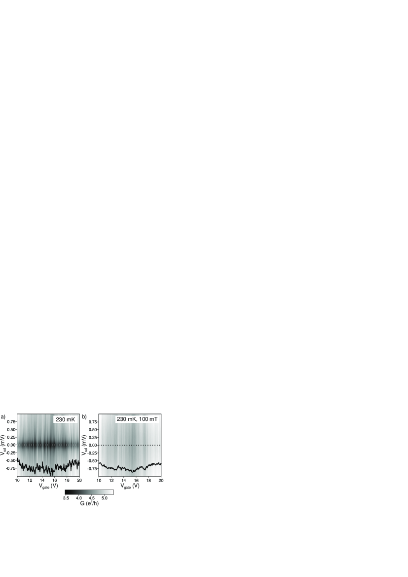
Figure 2 displays grey scale plots of in region (III) near the CNP as a function of and at 230 mK. In figure 2(a), the electrodes are in a superconducting state. Due to the superconducting gap transport is expected to be dominated by Andreev reflection at low bias voltage , where the factor 2 accounts for the two superconductors defining source and drain contacts. In this bias window the device displays a suppression , indicative for weakly coupled contacts. The fluctuations in as a function of are largest at zero bias and are reduced by an increased . When applying a small magnetic field, as shown in figure 2(b), the superconductivity is suppressed. Consequently, the fluctuations of at zero bias are visibly reduced.
In order to quantify the change in the conductance fluctuations originating from enhancement due to Andreev reflections, we investigate the standard deviation of the conduction, as a function of the bias voltage , as shown in Trbovic et al. (2010).
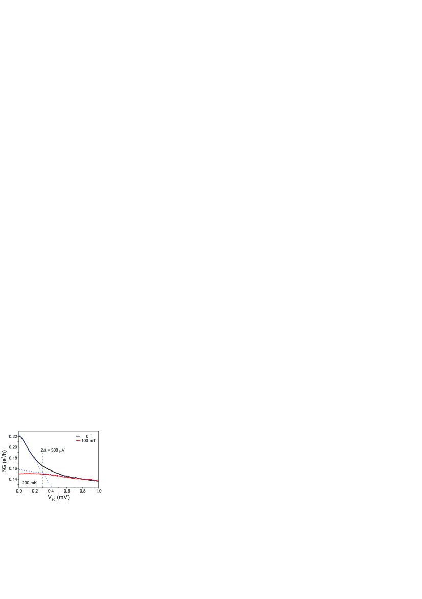
Figure 3 shows a plot of against near the CNP in (III). When the electrodes are in a superconducting state, the CF are largest at zero with 0.22 e2/h. With increasing the CF decrease and reach at 1 mV a value of 0.14 e2/h. By comparing the slopes of the steeply changing CF at small and the more slowly varying CF at larger , we can extract a crossover and thus a superconducting gap of 300 V. In the normal conducting state at 100 mT, the CF are about 0.14 e2/h at 1 mV, which coincides with the value of the superconducting electrodes. However, for 0.3 mV the CF in the normal state saturate at 0.15 e2/h. Thus the CF in the superconducting state are enhanced by a factor of up to 1.5 compared to the normal state.
When comparing the normal state fluctuations 0.15 e2/h to the theoretical Altshuler-Lee-Stone (ALS) value of e2/h 1.2 e2/h Rycerz et al. (2007), we find that the prediction is almost one order of magnitude larger than the measured value. One way to resolve this discrepancy is to assume that the phase coherence length is much shorter than the length of the device. Assuming that each segment of length is fluctuating independently, yields an overall reduced CF Trbovic et al. (2010). Applying this approach to the current values yields a phase coherence length of 300 nm. However, the fact that the measured CF is nearly doubled in the superconducting states suggests that almost all electrons are within the coherence length of one of the superconducting interface, hence . This in strong contradicting to the value of estimated from the normal state fluctuations.
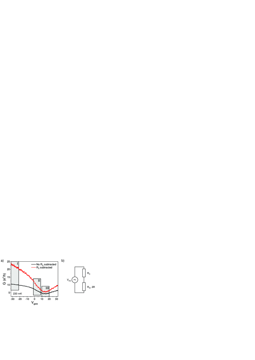
Another parameter which can reduce the apparent CF is a built-in series resistance . This is schematically shown in 4(b). The graphene part has the resistance which fluctuates with , whereas is assumed to be constant. In practice consists of the electrical lines in the measurement set-up, the input impedance of the IV converter and the resistance of the Al contact lines. In addition, it may also contain to some extent the contact resistance of the device Williams et al. (2009). All this is intrinsic to two-terminal measurements. We assume that is independent of the carrier concentration in the graphene flake. The subtraction of corrects the measured fluctuations, , by . By adding the known resistance of the measurement setup (measurement lines and IV converter) we arrive at a lower boundary of 1.35 k. An upper boundary of k. can be extracted from the quantum Hall effect, which due to the magnetic field measures the device in the normal state. has been deduced from the shifts of the Hall plateaus.
Figure 4(a) compares against at 230 mK with and without 1.35 k subtracted. As expected the correction results in the largest change at large doping when is large. The same is true for the CF, as we will show in the following.
In order to assess the sensitivity of the CF on the value of , we have investigated the dependence of the CF measured at 0 and 230 mK for different values, ranging from 0 to 2 k in regime (I) (high doping), (II) (intermediate doping), and (III) (CNP). Figure 5 shows the result. In order to calculate a B-spline was subtracted to account for the non-constant background of the graphene conductance . The absolute values of the CF are lower than the values found in figure 3, because there only a linear background was removed.
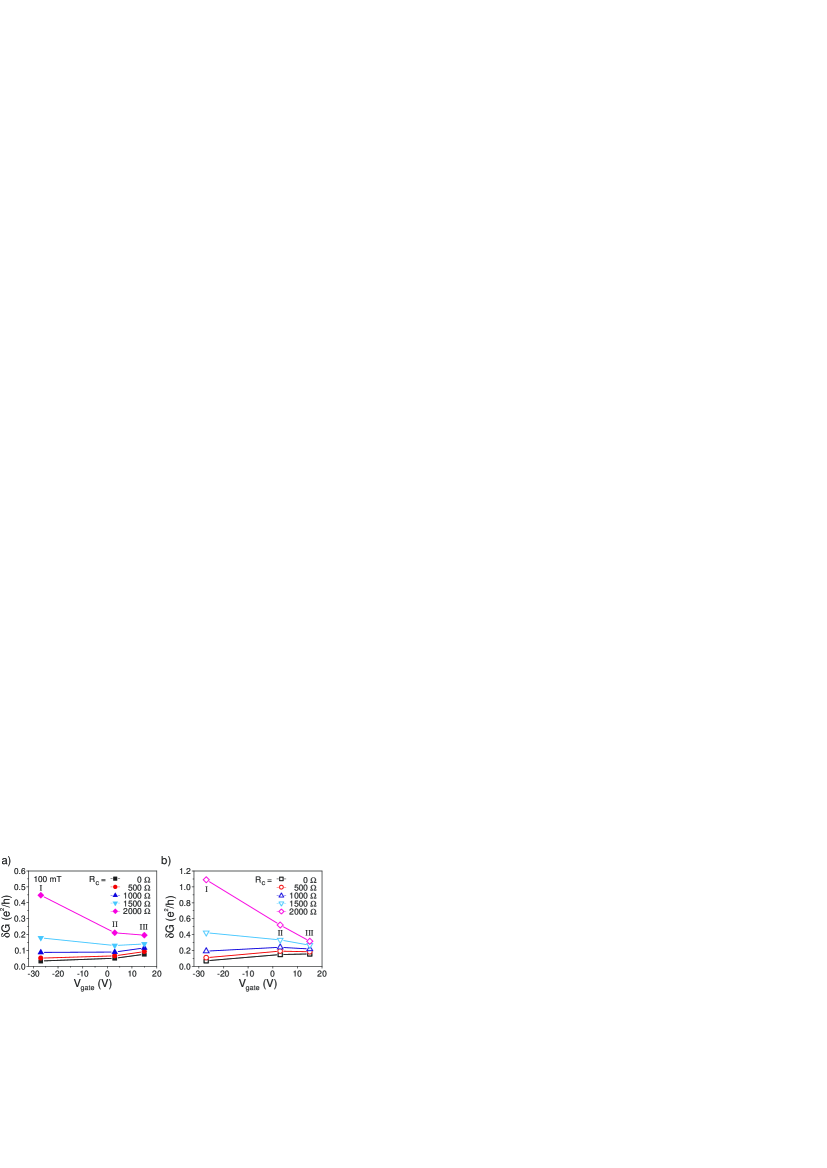
In figure 5(a) the electrical contacts are in a normal conducting state due to the application of a 100 mT magnetic field. The as measured data (no subtracted) shows the smallest CF which increase from 0.03 e2/h in (I) to 0.08 e2/h in (III). Around the series resistance that we estimated for our set-up (1.35 k - 1.5 k), the fluctuations are nearly independent of , with values of 0.14 e2/h in regimes (I) and (III). If 2 k is subtracted the CF in (I) reach 0.45 e2/h and are reduced to 0.2 e2/h in (III).
Without the subtraction of , the CF are minimal at large doping and increase near the CNP. When is subtracted the CF increase. However, they increase the most in region (I), less strong in region (II) and the weakest increase is in region (III). This can lead to a reversal of the dependence of the CFs on the .
The conductance fluctuations with superconducting contacts are plotted in figure 5(b). The measured data without any subtracted shows an increase from 0.07 e2/h in (I) to 0.16 e2/h near the CNP in (III). Again, for values of that lie within the estimates for our set-up, the CF vary only weakly with from 0.32 e2/h in (I) to 0.25 e2/h in (III). At higher values of the CF decrease significantly from (I) to (III).
Evidently, the superconductivity enhances the CF in all three regimes. In (I) and (III) the enhancement lies close to a factor of 2. Yet in regime (II) it appears to be consistently higher and reaches a factor of 3. In part this large enhancement factor originates from the resistance of the aluminium electrodes, which is approximately 100 in the normal state in our device. If we consider this difference, we find an enhancement factor of around 1.9 for (I) and (III), but still above 2 for regime (II).
In recent experiments contradicting observations were made. In Ojeda-Aristizabal et al. (2010) an increase of the CF near the CNP was seen, where the increase of the CF from high charge carrier concentration to near the CNP was attributed to the formation of electron-hole puddles. In contrast, a decrease of CF near the CNP was found in Staley et al. (2008); Chen et al. (2010). The changes in the CF were reported to be of a factor of 3 or larger. Gate independent CF were observed in Horsell et al. (2009). As in our device, Ojeda-Aristizabal et al. (2010) rely on two-terminal measurements, which include , whereas Staley et al. (2008); Chen et al. (2010) use a four-terminal set-up, where is irrelevant. As shown above, we can see all three gate dependences if we subtract . Nevertheless, for the range of that we estimate for our set-up, we find nearly no change in CF at high charge carrier density and near the CNP in our graphene device.
IV Conclusions
Using graphene devices with superconducting contacts, we have shown that CFs are enhanced in the superconducting relative to the normal state of the contacts. This enhancement amounts to a factor between 1.4 and 2 and thus suggests that all electrons in the device of length 1.3 m are within the coherence length of one of the two contacts where Andreev reflection occurs which is the origin of the doubling Beenakker (1995). The phase coherence length at 230 mK is therefore large and amounts to . We established a constant series resistor to account for our two-terminal measurement set-up and device and investigated its impact on the CF. For values of that we estimated for our set-up and device the CF remain smaller than e2/h. Furthermore, we investigated the dependence of the CF on the back-gate voltage . A strong dependence on is found. Without subtraction of the CF increase around the CNP compared to the CF at high doping. In the range of appropriate the CF are nearly independent of .
Acknowledgements.
This work is financially supported by the NCCR on Nanoscale Science, the NCCR on Quantum Science, the Swiss NSF and EU-FP7-IST project SE2ND. We are grateful to Markus Weiss and Romain Maurand for discussions.References
- Morozov et al. (2006) S. Morozov, K. Novoselov, M. Katsnelson, F. Schedin, L. Ponomarenko, D. Jiang, and A. Geim, Physical Review Letters 97, 16801 (2006).
- Heersche et al. (2007) H. B. Heersche, P. Jarillo-Herrero, J. B. Oostinga, L. M. Vandersypen, and A. F. Morpurgo, The European Physical Journal - Special Topics 148, 27 (2007), 10.1140/epjst/e2007-00223-7.
- Ojeda-Aristizabal et al. (2009) C. Ojeda-Aristizabal, M. Ferrier, S. Gueron, and H. Bouchiat, Phys. Rev. B 79, 165436 (2009).
- Skákalová et al. (2009) V. Skákalová, A. B. Kaiser, J. S. Yoo, D. Obergfell, and S. Roth, Phys. Rev. B 80, 153404 (2009).
- Trbovic et al. (2010) J. Trbovic, N. Minder, F. Freitag, and C. Schönenberger, Nanotechnology 21, 274005 (8 pp.) (2010).
- Geim and Novoselov (2007) A. K. Geim and K. S. Novoselov, Nat Mater 6, 183 (2007).
- McCann et al. (2006) E. McCann, K. Kechedzhi, V. I. Fal’ko, H. Suzuura, T. Ando, and B. L. Altshuler, Phys. Rev. Lett. 97, 146805 (2006).
- Rycerz et al. (2007) A. Rycerz, J. Tworzydlo, and C. W. J. Beenakker, EPL 79, 57003 (2007).
- Borunda et al. (2011) M. F. Borunda, J. Berezovsky, R. M. Westervelt, and E. J. Heller, ACS Nano 5, 3622 (2011), http://pubs.acs.org/doi/pdf/10.1021/nn103450d .
- Kharitonov and Efetov (2008) M. Y. Kharitonov and K. B. Efetov, Phys. Rev. B 78, 033404 (2008).
- Beenakker (1995) C. W. J. Beenakker, Mesoscopic Quantum Physics, edited by E. Akkermans, G. Montambaux, J.-L. Pichard, and J. Zin-Justin (1995).
- Novoselov et al. (2005) K. Novoselov, D. Jiang, F. Schedin, T. Booth, V. Khotkevich, S. Morozov, and A. Geim, Proc. Natl. Acad. Sci. U.S.A. 102, 10451 (2005).
- Ferrari et al. (2006) A. C. Ferrari, J. C. Meyer, V. Scardaci, C. Casiraghi, M. Lazzeri, F. Mauri, S. Piscanec, D. Jiang, K. S. Novoselov, S. Roth, and A. K. Geim, Phys. Rev. Lett. 97, 187401 (2006).
- Chen et al. (2008) J.-H. Chen, C. Jang, S. Adam, M. S. Fuhrer, E. D. Williams, and M. Ishigami, Nat Phys 4, 377 (2008).
- Williams et al. (2009) J. R. Williams, D. A. Abanin, L. DiCarlo, L. S. Levitov, and C. M. Marcus, Phys. Rev. B 80, 045408 (2009).
- Ojeda-Aristizabal et al. (2010) C. Ojeda-Aristizabal, M. Monteverde, R. Weil, M. Ferrier, S. Gueron, and H. Bouchiat, Phys. Rev. Lett. 104, 186802 (2010).
- Staley et al. (2008) N. Staley, C. Puls, and Y. Liu, Phys. Rev. B 77, 155429 (2008).
- Chen et al. (2010) Y.-F. Chen, M.-H. Bae, C. Chialvo, T. Dirks, A. Bezryadin, and N. Mason, Journal of Physics: Condensed Matter 22, 205301 (2010).
- Horsell et al. (2009) D. Horsell, A. Savchenko, F. Tikhonenko, K. Kechedzhi, I. Lerner, and V. Fal’ko, Solid State Communications 149, 1041 (2009), recent Progress in Graphene Studies.