Effect of phosphous-doped upon the electronic structures of single wall carbon nanotubes
Abstract
We studied Phosphorus-doped single wall carbon nanotubes (SWCNT) by using the First-Principle method based on Density Function Theory (DFT). The formation energy, total energy, band structure, geometry structure and density of states were calculated. We have found that the formation energy of the P-doped single carbon nanotube increases with its diameter. The total energy of carbon nanotubes in the same diameter decreases with the increasing doping concentration. The effects of impurity position on the impurity level were discussed in this paper. It is illustrated that the position of impurity level may depend on the C-P-C bond angle. According to the results, it is feasible to substitute a phosphorus atom for a carbon atom in SWCNT. It is also found that P-doped carbon nanotubes are n type semiconductors.
School of Physics & Telecommunication Engineering, South China Normal University, GuangZhou 510006, China Keywords:Single wall carbon nanotube, P-doped, First-Principle Calculation, formation energy, density of state
1 Introduction
Since the carbon nanotubes were discovered [1], they have attracted the attention of numerous research groups because of their outstanding mechanical and electronic properties. A single-wall carbon nanotube (SWCNT) can be described as a graphite sheet rolled into a cylindrical shape so that the structure is of one dimension [2] with a diameter of about 0.7-10.0 nm. Carbon nanotubes are regarded as the ultimate fiber with regard to its strength in the direction of the nanotubes axis [3]. Carbon nanotubes are regarded as the ultimate fiber with regard to its strength in the direction of the nanotubes axis , and its electronic structure can be either metallic or semiconducting depending on its diameter and chirality [4]. Carbon nanotubes have been studied in a wide range of areas, including field emitter for flat panel displays, microelectronics devices, chemic sensors [5] press sensors[6], etc. Doped carbon nanotubes have played a vital role in the electronic devices and nano-sensors fabricated with carbon nanotubes. There are many investigations on doped carbon nanotubes in theory such as boron-doped carbon nanotubes and N-doped carbon nanotubes. It is known that B impurities are injected in carbon nanotubes with small diameter easier than those with big diameter. The ionization potential (IP) of B-doped zigzag (10,0) carbon nanotubes is about 0.2 eV. The work function of N-doped carbon nanotubes is lower than that of pristine carbon nanotubes. Otherwise, work function and ionization potential of N-doped carbon nanotubes vary with the position of N impurities in carbon nanotubes. Both decrease on energy gap of semiconducting carbon nanotubes and increase in local density of states on Fermi energy level owing to the presence of impurities.
It is because carbon nanotubes behave as a metal or as a semiconductor depending on the chirality and diameter that it is hard to attain homogeneous carbon nanotubes in experiment. The doped carbon nanotubes will be P type or N type semiconductor, just as diamond film which is doped with phosphorus is N type semiconductor. P-doped diamond film has been synthesized with microwave inductive plasma chemic vapor deposition by Chen et al.[7]. They found that the filed emission current of P-doped diamond film has been increased sharply more than that of B-doped diamond film. Cruzsilva et al. [8] used a solution of ferrocene, triphenylphosphine, and benzylamine in conjunction with spray pyrolysis to synthesize phosphorus-nitrogen doped multiwall carbon nanotubes forming hetero-doped carbon nanotubes and did some theoretic calculation. However, they did not study the electronic structure further, such as how both the concentration of P impurity and the position of P atom in SWCNT affect the electronic structure, while we discuss this point in detail, right now.
As a new material of nanotechnology, it is necessary that carbon nanotubes should be doped with impurities. It is of a vital importance to study the effects of concentration on the total energy of carbon nanotubes and to predict the feasibility of attaining carbon nanotubes with different impurity concentrations. Different positions of P impurity in carbon nanotubes have different effects on the electronic structure of carbon nanotubes. So it is inevitable to study the doped form of P impurity and the effects of P impurity position on carbon nanotubes. It maybe provide some important theory for investigating the device applied to nano-integrate circuit in the future.
As far as I know, there is little theoretic calculation on P-doped SWCNT. But it is only to study the energy band structure and total energy without studying the effects of position of P impurity on the electronic structure. Considering the above important facts, P-doped SWCNT will be introduced in this letter, and the first principle calculation based density of function theory is carried out to explore the basic electronic structure characteris- tic of P-doped SWCNT by attaining the formation energy change of SWCNT after P presence and analyzing the effects of the position of P in SWCNT. There are three aspects to be calculated: the geometry structure and total energy of P-doped SWCNT with different diameters, the total energy of P-doped SWCNT with vari- ous impurity concentrations, and analysis of the interre- lated factor of position of impurities level induced by the position of P impurity. The formation energy varies with the diameter of P-doped SWCNT.
2 The model and method of calculation
All theoretical calculations in this letter are completed by Castep package [9] which is a state-of-the-art quantum mechanics-based program designed specifically for solid-state materials science and employs the density functional theory plane-wave pseudopotential method. It allows us to perform first-principles quantum mechanics calculations to explore the properties of crystals and surfaces in materials such as semiconductors, ceramics, metals, minerals, and zeolites, and it is available from Accelry Inc. It is the more precise calculation method to explore the electronic structure currently [10]. Many calculations in published papers [11], [12] have been completed by it. In this letter, we focus on zigzag tubes and arm- chair tube including (5,0), (6,0), (7,0), (8,0), (9,0) and (10,0) type tube, in whose cell there are 20, 24, 28, 32, 36, and 40 atoms, respectively. We substitute a C atom in carbon framework with a P atom. In order to study the effects of the impurity concentration upon SWCNT, we construct PC, PC, and PC tubes, respectively. The position of impurities is different. All of the models have been calculated by the First Principle Theory based on DFT. We have used the general-gradient potential approximation (GGA) [13] of PBE for exchange and correlation functional. GGA provides a better overall description of the electronic subsystem than the LDA func- tional’s in the framework of DFT because the LDA description tends to overbind atoms, so that the bond lengths and the cell volume are usually underestimated by a few percent and the bulk modulus is correspond- ingly overestimated. The calculations are expended us- ing plane waves basis with a cutoff energy of 470 eV, and we also use Normal-conserving pseudopotential [14], [15] to perform the interaction between ions and electrons. Geometry optimization is performed with convergence toleration of 210 eV/atom. The pressure on every atom is less than 0.05 eV/Å and stress is less than 0.1 GPa. We take 116 k points in the first Brillouin zone.
3 Results
3.1 The optimized geometry structure and total energy
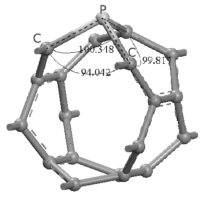
The geometry structure of P-doped SWCNTs with different diameters has been optimized. Figure 1 illustrates the structure of (5,0) P-doped SWCNT clearly. We can see that a C atom in hexagon of a carbon nanotube frame is substituted with a P atom. Because the P atom radius is bigger than C atom radius, the regular hexagon frame is distorted. The length of C-P bond is 1.79 Å. The angles of C-P-C is varied from 94.042°-100.348° just as described in Figure 1, which agrees with the results reported by Cruz-Silva [8]. P atom has been pushed out from the graphene layer in order to form a stable framework.
The formation energy[9] of the substitutional P impurity by comparing the total energy to that of a pristine SWCNT has been calculated to discuss the stability of a P-doped SWCNT. The formation energy can be defined by the following formula:
Here, and represent the total energies of a P-doped and pristine SWCNT, respectively, and represents the energy per atom in phosphorus. Because is constant, the above formula can be rewritten as
Table 1 indicates the relationship between the diameter of P-doped SWCNT and . It is noteworthy that increases with diameter in both zigzag and armchair tubes indicating that narrower tubes are more favorable for phosphorus doping, which is similar to the results of B-doped SWCNT reported by Koretsune et al. [16]. According to their theory, we think that in order to stretch the P-C bonds, the carbon atoms should be pushed or the P atom should be moved higher the graphite layer accompanied by symmetry breaking, when graphite layer is doped substitutionally with P atom. For the tubes with big curvature, P atom can be injected when the tubes are distorted slightly. However, for the tubes with small curvature they need to be distorted intensely. But we think that the important reason is the form of C-P bond. When graphite layer is doped with P atoms, P atoms interact with the nearby C atoms exhibiting sp2 and sp3 hybridization. But there is more sp3 hybridization in tubes with narrower diameter accompanied with lower energy. So, the P-doped SWCNT with narrow diameters is easily synthesized. We have calculated the total energy to discuss the sta- bility of P-doped SWCNT with different impurity concentrations. The relationship between impurity concentration and total energy is shown in Table 2. The total energy of doped SWCNT decreases when the impurity concentration increases, which indicates that it is easier to synthesize doped carbon nanotubes if the impurity concentration becomes higher.
| Diameter (Å) | (eV) |
|---|---|
| 3.91(5,0) | −179.79413 |
| 4.70(6,0) | −179.61113 |
| 5.48(7,0) | −179.08833 |
| 6.62(8,0) | −178.99062 |
| 7.05(9,0) | −178.69707 |
| 7.83(10,0) | −178.4553 |
According to Table 2, the total energy of P-doped SWCNT is lower than that of pristine SWCNT, which suggests that P-doped SWCNT is more stable than pristine SWCNT. So it is likely possible to synthesize P-doped SWCNT with substitutional doping in experiment.
| Type | |
|---|---|
| C20 | −3101.13 |
| PC19 | −3125.86 |
| C24 | −3724.84 |
| PC23 | −3749.25 |
| C28 | −4348.32 |
| PC27 | −4372.11 |
| C40 | −6217.37 |
| PC39 | −6240.39 |
| P2C38 | −6264.36 |
| P3C37 | −6287.33 |
3.2 The band structure and density of state
In order to study electrical characteristics of P-doped carbon nanotubes well, both band structure and density of states of (5,0), (7,0), (8.0) and (10,0) tubes, respectively are calculated. Figure2 shows the band structure of (5,0), (7,0), (8,0) and (10,0) P-doped SWCNT, respectively.
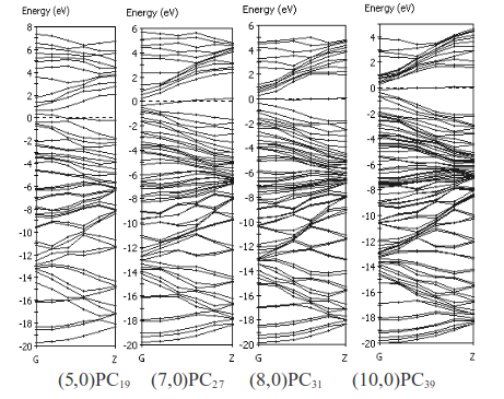
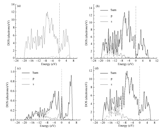
According to Figure 2, the presence of P introduces an impurity energy level near the Fermi energy level, while impurity energy levels of (5,0)PC, (7,0)PC, and (10,0)PC, respectively are closer to valence band top than to conduction band bottom across the Fermi energy level. But the impurity level of (8,0)PC crosses the Fermi energy in the middle of the gap between valence band top and conduction band bottom. Just as described in Figures 3(c) and 3(d), the electrons from p orbit belong to P atom without becoming bond. So they mainly contribute to the DOS near Fermi energy level. Each carbon atom has six electrons which occupy 1s, 2s and 2p atomic orbitals. The 2s orbital and two 2p orbitals are hybridized forming three sp2 hybridized orbitals. These hybrid orbitals form bonds. Each carbon atom has an excess electron which has been hybridized but forms a orbital perpendicular to the graphite sheet plane. According to Figure 3(d), although there are numerous electrons from p orbital to contribute to valence band and conduction band, there are also a few electrons from s orbital to contribute to valence band and conduction band. Besides, there are few electrons from s orbital near Fermi energy level contributing to valence band and conduction band [see Figure 3(b)]. According to the PDOS of P-doped SWCNT, however, just as described in Figure 3(d), there are a few electrons from s orbital near Fermi energy level. Therefore the electrons from s orbital are mainly from P atom. By comparing Figures 3(a) with 3(b), it is obvious that the peak in Fermi energy level mainly results from the impurity levels of P atoms. Figure 3(c) reveals that some peaks locating between -4 and 1 eV are mainly due to electrons from p orbitals of P impurities. But there are also a few electrons from s orbitals for those peaks. There is a mixing of p and s atomic orbitals at the same level, which leads to that p orbital and s orbital are hybridized. The peak above Fermi energy level is also mainly due to the result that p orbital and s orbital are hybridized.
The band structure of pristine (10,0) SWCNT and P-doped SWCNT is shown in Figures 4(a)-(d). Pristine zigzag (10,0) carbon nanotubes have the D10h symmetry [17], [18], [19]. Figure 4(a) shows the band structure of pristine (10,0) carbon nanotubes, from which we can see that zigzag (10,0) carbon nanotube is direct-gap semiconductor and that the energy bands show a large doubly degeneracy at the zone boundary. The band gap is 0.57 eV approximately, which is similar to that reported in some paper[14]. Valence band top and conduction band bottom correspond to energy bonding band and energy anti-bonding band respectively. Figures 4(b)-(d) are the energy band structures of PC39, P2C38 and P3C37, respectively and there are impurity energy levels near Fermi energy level. Figure 4(b) shows clearly that impurity energy levels cross the Fermi energy level and the impurity energy level is closer to valence band top than to conduction band bottom. It also shows that Fermi energy is closer to valence band top. In Figure 4(c) we can see that there are two impurity energy levels. One crosses Fermi energy but the other is under Fermi energy level. There are three impurity energy levels shown in Figure 4(d). One is between Fermi energy level and conduction band bottom, the other is across Fermi energy and the last one is between Fermi level and valence band top.
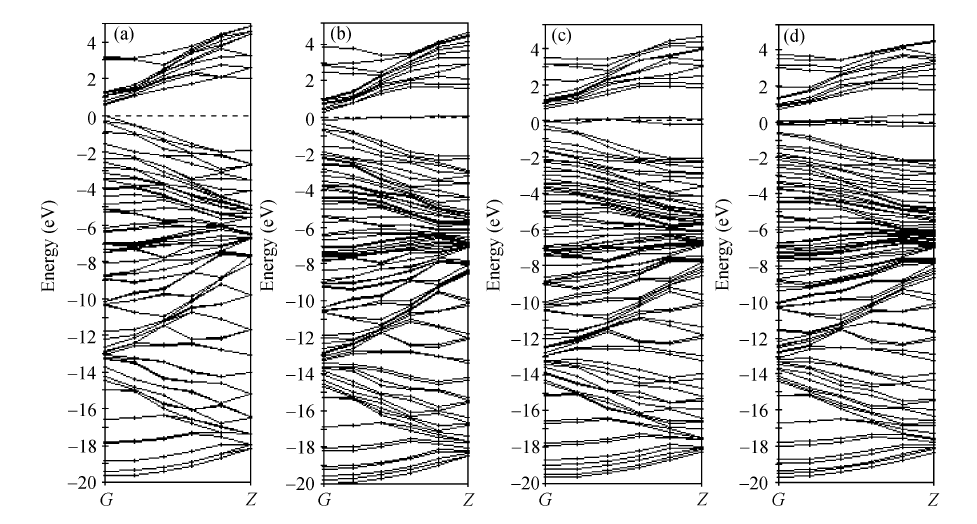
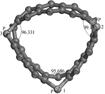
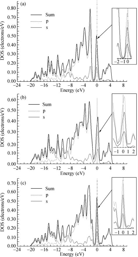
Figure 5 shows the structure of P3C37 SWCNT and the different positions of P atom. The DOS of No. 1, No. 2 and No. 3 atoms are shown in Figures 6(a)-(c), respectively. The peak located at the Fermi energy level left is an impurity peak just as Figure 6(a) shows. It illustrates that there is an impurity energy level under the Fermi energy level. The reason for that is the C-P-C bond angle with 95.686° which is close to the typical angle of sp3 hybridization. It suggests that there may be sp3 hybridization between C atoms and P atoms to lead to bond. So an impurity energy level is introduced between Fermi energy level and valence band top. There is a sharp peak at the Fermi energy level right shown in Figure 6(b) which corresponds to the DOS of No. 2 P atom. The C-P-C angle composed with No. 2 P atom and C atoms is 99.1° (see Figure 5), so there may be no sp3 hybridization between No. 2 P atom and nearby C atoms. The P atom has one valence electron more than C atom. Therefore an impurity energy level is generated between Fermi energy and conduction band bottom. The C-P-C angle composed with No. 3 P atom and C atoms is among the angle composed with No. 1 P atom and C atoms and the angle composed with No. 2 P atom and C atoms. Therefore, the No. 3 P impurity energy level is located between No. 1 P and No. 2 P impurity energy level, which is described well in Figure 4(d). Other P-doped SWCNTs have the same characteristics as (10,0) P-doped SWCNT. According to Figure 6, it is noticeable that the peaks of P impurity near Fermi energy mainly result from that the s and p atomic orbitals of P atom are hybridized.
4 Conclusion
We have studied the basic electronic structure of P-doped SWCNT by the First Principle Theory based DFT. The formation energy of P-doped SWCNT is related to the diameters. The narrower diameters are, the lower formation energy is. Therefore, the system gets more stable. It can be concluded that the total energy of P-doped SWCNT is lower than that of pristine SWCNT, and the total energy will get lower with the impurity concentration increase by analyzing the total energy of P-doped carbon nanotubes. It is feasible to substitute a carbon atom with a phosphorus atom in SWCNT in terms of theory. By analyzing of DOS and PDOS, we can see that the DOS near Fermi energy level attribute to the electronics from the p orbital and the impurity energy level may be affected by the C-P-C angle and the sp hybridization leads to the impurity peak, so the presence of P atom affects the physic property of SWCNT in a certain sense. Doping is important for chemic and physic performance of SWCNT as the promising nano-material in the future. The P-doped carbon nanotubes enrich the material for fabricating nano-device. The other significance of this paper is that it may provide some theory for studying the device applied to nano-integrated circuits in the future.
References
- [1] S. Iijima et al. Helical microtubules of graphitic carbon. nature, 354(6348):56–58, 1991.
- [2] M. Jose-Yacaman, M. Miki-Yoshida, L. Rendon, and J. G. Santiesteban. Catalytic growth of carbon microtubules with fullerene structure. Applied physics letters, 62(2):202–204, 1993.
- [3] G. Overney, W. Zhong, and D. Tomanek. Structural rigidity and low frequency vibrational modes of long carbon tubules. Zeitschrift fÃŒr Physik D Atoms, Molecules and Clusters, 27(1):93–96, 1993.
- [4] M. S. Dresselhaus, G. Dresselhaus, and R. Saito. Physics of carbon nanotubes. Carbon, 33(7):883–891, 1995.
- [5] J. Cao, Q. Wang, and H. Dai. Electromechanical properties of metallic, quasimetallic, and semiconducting carbon nanotubes under stretching. Physical review letters, 90(15):157601, 2003.
- [6] R. J Grow, Q. Wang, J. Cao, D. Wang, and H. Dai. Piezoresistance of carbon nanotubes on deformable thin-film membranes. Applied Physics Letters, 86:093104, 2005.
- [7] C. F Chen, C. L Tsai, and C. L Lin. Electronic properties of phosphorus-doped triode-type diamond field emission arrays. Materials chemistry and physics, 72(2):210–213, 2001.
- [8] E. Cruz-Silva, D. A Cullen, L. Gu, J. M. Romo-Herrera, et al. Heterodoped nanotubes:theory, synthesis, and characterization of phosphorus-nitrogen doped multiwalled carbon nanotubes. ACS nano, 2(3):441–448, 2008.
- [9] M. D. Segall, P. J.D Lindan, M. J. Probert, C. J. Pickard, P. J. Hasnip, S. J. Clark, and M. C. Payne. First-principles simulation: ideas, illustrations and the CASTEP code. Journal of Physics: Condensed Matter, 14:2717, 2002.
- [10] K. Watanabe, M. Sakairi, H. Takahashi, K. Takahiro, S. Nagata, and S. Hirai. Formation of composite oxide films on aluminum by sol-gel coating and anodizing-for the development of high performance aluminum electrolytic capacitors. ELECTROCHEMISTRY-TOKYO-, 69(6):407–413, 2001.
- [11] X. H. Yan, Y. Xiao, J. W. Ding, Z. H. Guo, Y. R. Yang, and D. L. Wang. Density functional calculations of carbon nanotubes: Behavior of double-walled nanotubes compared to classical cylindrical capacitors. Physical Review B, 75(19):195442, 2007.
- [12] J. Zhao, H. Park, J. Han, and J. P Lu. Electronic properties of carbon nanotubes with covalent sidewall functionalization. The Journal of Physical Chemistry B, 108(14):4227–4230, 2004.
- [13] J. P Perdew, K. Burke, and M. Ernzerhof. Generalized gradient approximation made simple [phys. rev. lett. 77, 3865 (1996)]. Physical Review Letters, 78(7):1396–1396, 1997.
- [14] N. Troullier and J. L Martins. Efficient pseudopotentials for plane-wave calculations. Physical Review B, 43(3):1993, 1991.
- [15] L. Kleinman and D. M. Bylander. Efficacious form for model pseudopotentials. Physical Review Letters, 48(20):1425–1428, 1982.
- [16] T. Koretsune and S. Saito. Electronic structure of boron-doped carbon nanotubes. Physical Review B, 77(16):165417, 2008.
- [17] R. Li, W. Ji, and J. Lin. Effects of nitrogenation on single-walled carbon nanotubes within density functional theory. Physical Review B, 76(19):195406, 2007.
- [18] H. Pan, Y. P. Feng, and J. Y. Lin. Ab initio study of OH-functionalized single-wall carbon nanotubes. Physical Review B, 70(24):245425, 2004.
- [19] R. Saito, G. Dresselhaus, M. S Dresselhaus, et al. Physical properties of carbon nanotubes, volume 3. Imperial College Press London, 1998.