Influence of strain on anisotropic thermoelectric transport of and
Abstract
On the basis of detailed first-principles calculations and semi-classical Boltzmann transport, the anisotropic thermoelectric transport properties of and under strain were investigated. It was found that due to compensation effects of the strain dependent thermopower and electrical conductivity, the related powerfactor will decrease under applied in-plane strain for , while being stable for . A clear preference for thermoelectric transport under hole-doping, as well as for the in-plane transport direction was found for both tellurides. In contrast to the electrical conductivity anisotropy, the anisotropy of the thermopower was almost robust under applied strain. The assumption of an anisotropic relaxation time for suggests, that already in the single crystalline system strong anisotropic scattering effects should play a role.
pacs:
31.15.A-,71.15.Mb,72.20.Pa,72.20.-iI Introduction
Thermoelectric (TE) materials are used as solid state energy devices which convert waste heat into electricity or electrical power directly into cooling or heating Sales (2002); Majumdar (2004); Böttner et al. (2006). Telluride based thermoelectrics, e.g. the bulk materials bismuth () and antimony telluride () and their related alloys, dominate efficient TE energy conversion at room temperature for the last 60 years Goldsmid et al. (1958); Venkatasubramanian et al. (2001). The materials TE efficiency is quantified by the figure of merit
| (1) |
where is the electrical conductivity, the thermopower, and are the electronic and phononic contribution to the thermal conductivity, respectively. From Eq. 1 it is obvious, that a higher ZT is obtained by decreasing the denominator or by increasing the numerator, the latter being called powerfactor . While bulk and show T values smaller 1 and applications have been limited to niche areas, a break-trough experiment of Venkatasubramanian et al. showed a remarkable for p-type/n-type superlattices (SL) composed of the two bulk tellurides Venkatasubramanian et al. (1999); Venkatasubramanian (2000); Venkatasubramanian et al. (2001). With the availability of high-ZT materials, many new applications will emerge Majumdar (2004). The idea of thermoelectric SL follows the idea of phonon-blocking and electron-transmitting at the same time. It suggests that cross-plane transport along the direction perpendicular to the artificial interfaces of the SL reduces phonon heat conduction while maintaining or even enhancing the electron transport Böttner et al. (2006). While some effort in experimental research was done Beyer et al. (2002); Böttner et al. (2004); König et al. (2011); Liao et al. (2010); Peranio et al. (2006); Touzelbaev et al. (2001), only a few theoretical works discuss the possible transport across such SL structuresPark et al. (2010); Li et al. (2004). While Park et al.Park et al. (2010) discussed the effect of volume change on the in-plane thermoelectric transport properties of , and their related compound, Li et al.Li et al. (2004) focussed on the calculation of the electronic structure for a -SL, stating changes of the mobility anisotropy estimated from effective masses.
Superlattices are anisotropic by definition and even the telluride bulk materials show intrinsic anisotropic structural and electronic properties. However, investigations of Venkatasubramanian et al. found a strong decrease for the mobility anisotropy and the thermoelectric properties for the -SL at certain periods. The reason for this behaviour is still on debate and could be related to strain effects which are induced by the epitaxial growth of the -SL. To extend previous works Scheidemantel et al. (2003); Thonhauser et al. (2003); Huang and Kaviany (2008) and to clarify the open question on the reduced anisotropy, we are going to discuss in this paper the anisotropic electronic transport in bulk and and the possible influence of strain in epitaxially grown SL on the TE properties.
For this purpose the paper will be organized as follows. In section II we introduce our first principle electronic structure calculations based on density functional theory and the semi-classical transport calculations based on the solution of the linearized Boltzmann equation. With this, we discuss the thermoelectric transport properties, that is electrical conductivity, thermopower and the related powerfactor, of unstrained and with a focus on their directional anisotropies. While in epitaxially grown -SL the atoms near the interfaces may be shifted from their bulk positions due to the lattice mismatch and the changed local environment, we modelled with the experimental lattice parameters and interatomic distances of , and vice versa. We assume that from these two limiting cases one could estimate the effect of the interface relaxation on the electronic and transport properties in -SL. With that structural data we first analyse in section III the anisotropic thermoelectric properties of the unstrained bulk systems, while in section IV a detailed view on the influence of strain, which may occur in -SL, on the electronic transport of these tellurides is given. Throughout the paper we quote () as strained, if it is considered in the lattice structure of (). As in the SL p-type, as well as n-type, transport was reported, we discuss the concentration dependence for both types of carriers on the transport properties.
II Methodology
For both bismuth and antimony telluride we used the experimental lattice parameters and relaxed atomic positions Lan (1998) as provided for the rhombohedral crystal structure with five atoms, i.e. one formula unit, per unit cell belonging to the space group (). The related layered hexagonal structure is composed out of three formula units and has the lattice parameters Å, Å, and Å, Å, for and , respectively. In fact, the main difference between the lattices of and is a decrease of the in-plane lattice constant with an accompanied decrease in cell volume. So, a change between the two lattice constants can be related to either compressive or tensile in-plane strain. This is very similiar to the approach by Park et al.Park et al. (2010), while omitting computational relaxation of internal atomic positions.
Our electronic structure calculations are performed in two steps. In a first step the detailed band structure of the strained and unstrained ans was obtained by first principles density functional theory calculations (DFT), as implemented in the fully relativistic screened Korringa-Kohn-Rostoker Greens-function method (KKR) Gradhand et al. (2009). Within this approach the Dirac-equation is solved self-consistently and with that spin-orbit-coupling is included. Exchange and correlation effects were accounted for by the local density approximation (LDA) parametrized by Vosco, Wilk, and Nusair Vosko and Wilk (1980). A detailed discussion on the influence of strain on the band structure topology of and is recently published B. Yu. Yavorsky, N. F. Hinsche, I. Mertig and P. Zahn (2011).
With the well converged results from the first step we obtain the thermoelectric transport properties by solving the linearized Boltzmann equation in relaxation time approximation (RTA) within an in-house developed Boltzmann transport code Mertig (1999); Zahn et al. (1995); Hinsche et al. (2011). Boltzmann transport calculations for thermoelectrics have been carried out for quite a long time and show reliable results for metals Vojta et al. (1992); Yang et al. (2008); Barth et al. (2010) as well as for wide- and narrow gap semiconductors Singh (2010); Parker and Singh (2010); May et al. (2009); Lee et al. (2011); Hinsche et al. (2011). TE transport calculations for bulk Huang and Kaviany (2008); Lee and von Allmen (2006); Park et al. (2010); Situmorang and Goldsmid (1986) and Thonhauser (2004); Thonhauser et al. (2003); Park et al. (2010) were presented before. Here the relaxation time is assumed to be constant with respect to wave vector k and energy on the scale of . This assumption is widely accepted for metals and highly doped semiconductors. Most of the presented results are in this high-doping regime. Within the RTA the transport distribution function (TDF) Mahan and Sofo (1996) and with this the generalized conductance moments are defined as
| (2) |
, denote the group velocities in the directions in the hexagonal basal plane and perpendicular to it, respectively. Within here the group velocities were obtained as derivatives along the lines of the Blöchl mesh in the whole Brillouin zoneB. Yu. Yavorsky, N. F. Hinsche, I. Mertig and P. Zahn (2011). A detailed discussion on implications and difficulties on the numerical determination of the group velocities in highly anisotropic materials is currently published elsewhereP. Zahn, B. Yu. Yavorsky, N. F. Hinsche and I. Mertig (2011). As can be seen straight forwardly, the electrical conductivity in- and cross-plane is then given by
| (3) |
and the temperature- and doping-dependent thermopower states as
| (4) |
for given chemical potential at temperature and extrinsic carrier concentration determined by an integration over the density of states
| (5) |
where is the conduction band minimum and is the valence band maximum. The energy range has to be taken sufficiently large to cover the tails of the Fermi-Dirac distribution function and to ensure convergence of the integrals in eq. 2 and 5 Hinsche et al. (2011). The k-space integration of eq. 2 for a system with an intrinsic anisotropic texture is quite demanding. In previous publications P. Zahn, B. Yu. Yavorsky, N. F. Hinsche and I. Mertig (2011); B. Yu. Yavorsky, N. F. Hinsche, I. Mertig and P. Zahn (2011) we stated on the relevance of adaptive integration methods needed to reach convergence of the energy dependent TDF. Especially in regions close to the band edges the anisotropy of the TDF requires a high density of the k-mesh. Here, convergence tests for the transport properties showed that at least 150 000 k-points in the entire BZ had to be included for sufficient high doping rates (), while for energies near the band edges even more than 56 million k-points were required to reach the analytical values for the conductivity anisotropies at the band edges111The analytical value of the ratio at the band edges was obtained by scanning the energy landscape near the conduction band minimum and valence band maximum fitting the dispersion relation in terms of an effective mass tensor. A detailed description is given in a recent publication by Ref. B. Yu. Yavorsky, N. F. Hinsche, I. Mertig and P. Zahn, 2011. Within the RTA, from comparison of the calculated electrical conductivities (eq. 3) with experiment it is possible to conclude on the directional anisotropy of . For the thermopower S (eq. 4) the dependence of the TDF on the energy is essential. That is, not only the sloop of the TDF, moreover the overall functional behaviour of the TDF on the considered energy scale has to change to observe an impact on the thermopower. The calculations in this paper aim to cover band structure effects and not scattering specific impacts by an energy- and state-dependent relaxation time.
III Anisotropic thermoelectric properties of unstrained and
In order to understand the experimental findings on the in-plane and cross-plane transport of the -SL, in the following section the anisotropies of the electrical conductivity, the thermopower and the related powerfactor of bulk and are discussed. Even though the behaviour of is strongly p-type with a extrinsic carrier concentration of ,Rowe (1995) we also discuss the related n-doped case, as in -SL n- as well as p-doping was reported. Bulk is known to be inherent electron conducting, while hole doping is experimentally achievable for bulk systems Delves et al. (1961); Goldsmid et al. (1958); Jeon et al. (1991); Kaibe (1989).

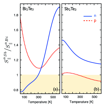
Figure 2 shows the variation of the anisotropic thermopower for unstrained and in a wide temperature range. The extrinsic charge carrier concentration of and was fixed to and , respectively. As a reference experimental values for both single crystalline materials at the same doping conditions are given and an excellent agreement can be stated. It is worth noting, that within eq. 4 the calculation of the thermopower is completely free of parameters. For the in-plane thermopower reaches a maximum of at , while the maximum for the hole-doped case is shifted to slightly higher temperatures of with a maximum values of . We note, that the temperature of the maximum is slightly overestimated. This might be caused by the missing temperature dependence of the energy gap, which was determined as for unstrained . The anisotropy of the thermopower is more pronounced for the p-doped case. Here the cross-plane thermopower is for the given doping always larger than the in-plane part . The anisotropy is about at 100K, evolving to and at 300K and 500K, respectively. The sole available experimental data show no noticeable anisotropy for the thermopower in the hole-doped case Stordeur and Kühnberger (1975). For the electron-doped case the situation is more sophisticated. While upto 340K the overall anisotropy is rather small, with values , a considerable decrease of at higher temperatures leads to high values of for temperatures above 400K. This tendency could also be revealed by experiments Zhitinskaya et al. (1976); Müller (1998). The crossing point of and near room temperature could explain the fact of varying measured anisotropies for the thermopower at 300K. Here anisotropy ratios of were reported Kaibe (1989); Müller (1998). The maximum peak of the thermopower near room temperature can be explained by the position of the chemical potential as a function of temperature at a fixed carrier concentration. For T much smaller than 300K the chemical potential is located in either the conduction- or valence band with the tails of the Fermi-Dirac-distribution in eq. 2 only playing a subsidiary role. For rising temperatures the chemical potential shifts towards the band edges and maximizes. At these conditions the conduction is mainly unipolar. For higher temperatures the chemical potential shifts into the bandgap and conduction becomes bipolar leading to a reduced thermopower. For the case of , shown in fig. 2(b), the situation is different. Due to the ten times higher inherent doping and the smaller energy gap of , the chemical potential is located deeply in the bands for the whole relevant temperature range. Therefore the functional behaviour can be understood in terms of the well known Mott relation, where equation 4 qualitatively coincides with for the thermopower in RTA Cutler and Mott (1969). With increasing temperature the thermopower increases almost linearly, showing values of and at 300K for p- and n-doping, respectively. The anisotropy of the thermopower for the hole-doped case is around , almost temperature-independent and slightly underestimates the available experimental values Simon and Eichler (1981); Langhammer et al. (1982). While for the electron-doped case the absolute values of the in-plane thermopower are comparable to those of the hole-doped case, the anisotropies are rather large. The anisotropy varies only weakly on temperature showing over the hole temperature range. While bulk states a strong p-character due to inherent defects, we note here again, that n-doping is available in heterostructures combining and Venkatasubramanian et al. (2001).
A strongly enhanced cross-plane thermopower could lead to a strongly enhanced powerfactor , if the cross-plane electrical conductivity is maintained at the bulk value.
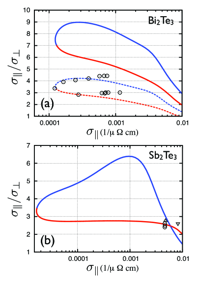
For this purpose the anisotropy of the electrical conductivity in dependence on the in-plane conductivity for unstrained and is shown in Figure 3. The temperature is fixed at 300K, blue and red lines refer to electron- and hole-doping, respectively. From comparison with experimental data 222The calculated dependencies of the electrical conductivity on the thermopower and the electrical conductivity on the applied doping were matched to fit experiments from Ref. Delves et al., 1961; Goldsmid et al., 1958; Langhammer et al., 1982., the in-plane relaxation time is determined to be and for and , respectively. With that we find strong anisotropies for the electrical conductivity , clearly preferring the in-plane transport in both bulk tellurides. For the strongly suppressed cross-plane conduction p-type conduction is more favoured than n-type conduction. For the pure band structure effects (solid lines in Figure 3(a)) overestimate the measured anisotropy ratio Delves et al. (1961) of the electrical conductivity. With an assumed anisotropy of the relaxation time of the experimental values are reproduced very well. That means, scattering effects strongly affect the transport and electrons travelling along the basal plane direction are scattered stronger than electrons travelling perpendicular to the basal plane. The origin of this assumed anisotropy has to be examined by defect calculations and resulting microscopic transition probabilities and state dependent mean free path vectors. It is well known, that in mainly anti-site defects lead to the inherent conduction behaviour Müller (1998); Rowe (1995); Cho et al. (1999). We have shown elsewhere P. Zahn, B. Yu. Yavorsky, N. F. Hinsche and I. Mertig (2011), that the integration of the transport integrals eq. 2 in anisotropic k-space requires large numeric effort. Tiny regions in k-space close to the band gap have to be scanned very carefully and the texture in k-space has a drastic influence on the obtained anisotropy values, if integrals are not converged with respect to the k-point density. As shown, some integration methods tend for the given k-space symmetry to underestimate the ratio in a systematic manner and therefore would shift anisotropy closer to the experimental observed values, without representing the real band structure effects. For unstrained the electrical conductivity anisotropy is highest for low values of , i.e. small amounts of doping and bipolar conduction. For larger charge carrier concentrations, i.e. the chemical potential shifts deeper into either conduction or valence band, the in-plane conductivity increases and the ratio decreases. Values for will lower from 7 to 2 for p-type conduction and 9 to 3 for n-type conduction. However, cross-plane electrical transport is always more suppressed for n-type carrier conduction, which also holds for unstrained . As shown in Figure 3(b) is almost doping independent for hole-doping, showing an anisotropy of around 2.7 in very good agreement with experiment (circle and triangles in fig. 3 from Ref. Simon and Eichler, 1981; Langhammer et al., 1982; Jacquot et al., 2010). In this case no anisotropic relaxation times had to be assumed. For electron doping the ratio is clearly higher, evolving values of 3.5 to 6 for rising in-plane conductivity. The dependence of the anisotropy ratio on the applied doping, i.e. changing , can be directly linked to the functional behaviour of the TDF near band edges, which is crucially influenced by the topology of the band structure B. Yu. Yavorsky, N. F. Hinsche, I. Mertig and P. Zahn (2011).
IV Anisotropic thermoelectric properties of strained and
Before the influence of in-plane strain on the resulting powerfactor will be discussed, we will first note on the strain induced changes of the components electrical conductivity and thermopower. In Figure 4 the anisotropy of the electrical conductivity is shown for both in the lattice constant of , i.e. under biaxial compressive in-plane strain (Figure 4(a)), and in the lattice constant of , i.e. under biaxial tensile in-plane strain (Figure 4(b)).
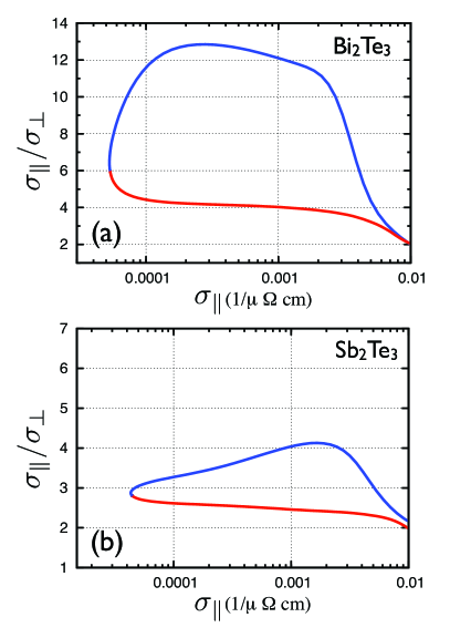
For the compressive in-plane strain causes an increase of the the band gap by around 23% yielding . While the anisotropy for hole doping (red lines in fig. 4(a)) decreases to around 4 and is almost constant under varying doping level, the ratio considerably raises under electron doping to values up to 13 for , corresponding to electron charge carrier concentrations of . This concludes, that the cross-plane electrical conductivity of under compressive in-plane strain will be noticeably enhanced for p-doping, but drastically suppressed for n-doping. Such a compressive in-plane strain could be introduced by either a substrate with smaller in-plane lattice constant, e.g. GaAs-[111] with Å, or a considerable amount of in the -SL. For tensile in-plane strained the impact on the electrical conductivity ratio is less prominent. As shown in figure 4(b) at hole doping is only marginally altered compared to the unstrained case (comp. fig. 3(b)). Meanwhile decreases noticeably for n-type doping yielding about 3 at low and low electron charge carrier concentrations, and slightly higher values of for higher doping. Overall, the tensile strain reduces the electrical conductivity anisotropy by a factor of about 1.5, directly leading to an enhanced electrical conductivity along the z-axis of single crystal . We note, that tensile in-plane strain opens the gap remarkably by around 56% compared to the unstrained case to a value of . Furthermore, such tensile strain could be incorporated by using either a substrate with larger in-plane lattice constant, e.g. PbTe-[111] with Å, or a higher fractional amount of in -SL.
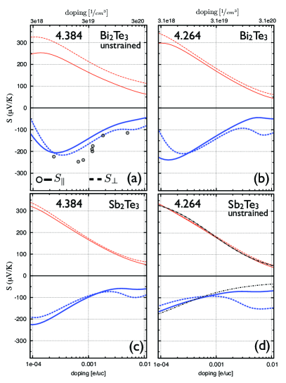
In Figure 5(a), (d) ((b), (c)) the doping dependent anisotropic thermopower of unstrained (strained) and at room temperature is shown, respectively. Blue thick (red thin) solid lines represent the in-plane thermopower under electron doping (hole doping). The corresponding cross-plane thermopower is shown as a dashed line. The black dashed-dotted lines in fig. 5(d) emphasize the expected doping dependent behaviour of the thermopower for parabolic bands, following the Pisarenko-relationIoffe (1960). For both tellurides we found, that the anisotropy of the thermopower shows a weak dependence on the strain state. However, for strained (see fig. 5(b)) the thermopower anisotropy under hole doping almost vanishes, leading to . It is worth noting, that the anisotropy of the thermopower is less pronounced for hole doping, than for electron doping for and in both strain states. As shown by the black dashed-dotted lines in fig. 5(d), the dependency of the thermopower on the charge carrier concentration differs from the Pisarenko-relationIoffe (1960) under sufficient high electron doping. This indicates, that the nonparabolicity of the energy bands has a noticeable impact in the investigated doping regime and should not be omitted by applying parabolic band models.
Actually, changes for the absolute values of the thermopower can be found for both telluride systems under applied strain.
In fig. 6 the relative change for the in-plane component for both tellurides under in-plane strain is given. To compare the changes with the lattice constant, we relate the in-plane thermopower at the smaller lattice constant to the value at the larger lattice constant for both compounds. The doping was fixed to for and for as done for fig. 2. Figure 6(a) shows, that in the relevant temperature range between 350K and 450K the thermopower increases for under compressive strain for both p and n doping by about 15-20%. For a decrease is expected under tensile strain at electron doping and nearly no change under hole doping (see Figure 6(b)). With nearly all values above 1 for , as well as for , it is obvious, that higher values of the thermopower require a smaller unit cell volume. One can expect, that the volume decrease causes a larger density of states and thus a shift of the chemical potential towards the corresponding band edge, connected with an increase of the thermopower S. However Park et al.Park et al. (2010) reported an unexpected increase of 16% for the in-plane thermopower of under p-doping (T=300K, ) if the material is strained into the structure. In the same doping and temperature regime we find a slight decrease of 4% for .
Comprising the statements on the electrical conductivity and the thermopower, the related powerfactor for both tellurides in their bulk lattice and in the strained state are compared in fig. 7. It is well known, that optimizing the powerfactor of a thermoelectric always involves a compromise on the electrical conductivity and the thermopower Snyder and Toberer (2008). Due to the interdependence of and it is not advisable to optimize the powerfactor by optimizing its parts.
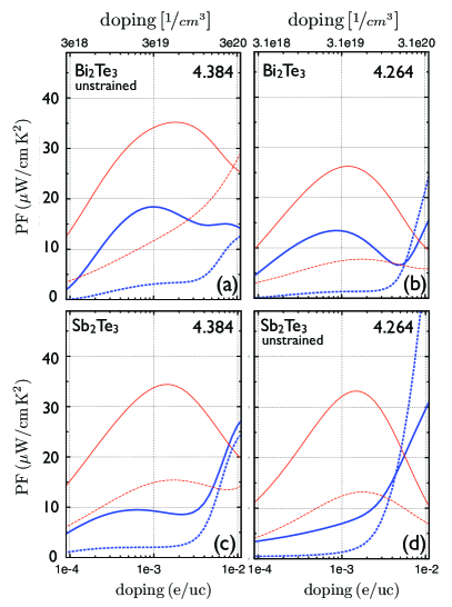
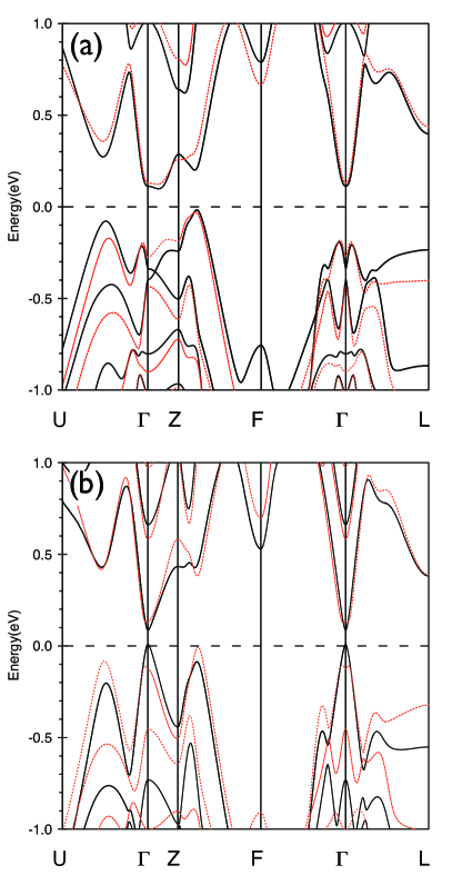
In Figure 7(a) and (d) the doping dependent anisotropic powerfactor of unstrained and at room temperature is shown, respectively. Blue thick (red thin) solid lines represent the in-plane powerfactor under electron doping (hole doping). The corresponding cross-plane powerfactor is shown as a dashed line. Under p-doping both unstrained materials show a maximum powerfactor near carrier concentrations of . Absolute values of and were found for unstrained and , respectively, which is in good agreement to experimental and theoretical findings Nurnus (2001); Böttner et al. (2004); Park et al. (2010). Under electron doping the absolute values of (thick blue lines in fig. 7) were found to be distinctly smaller. This is due to smaller absolute values of the thermopower for electron doping compared to hole doping (see Figure 2) and apparently smaller in-plane electrical conductivities at fixed carrier concentrations. As a result, a powerfactor of and can be stated for unstrained and , respectively, under optimal electron doping. We notice, that the powerfactor for unstrained is monotonically increasing for electron carrier concentrations of . This behaviour can be linked to a deviation of from the Pisarenko-relation under electron doping. While it is expected, that the thermopower will decrease for increasing carrier concentration, was found to be almost constant in an electron doping range of (see fig. 5(d)). For the investigated electron doping range of the chemical potential at 300K is located around above the VBM. As can be seen from the band structure for unstrained in fig. 1(b) (black, solid lines) flat non-parabolic bands near the high symmetry point Z dominate in this energy region and most likely lead to an increased thermopower. This feature is more pronounced for unstrained , than for strained (red, dashed lines in fig. 1(b)). Similar statements can be done for strained and unstrained (see fig. 1(a)). We note, even though this picture is convincing, it is difficult to link such specific anomalies to the band structure on high symmetry lines, as the underlying TDF is an integral quantity over all occupied states in the BZ.
Under applied in-plane compressive strain for (ref. Figure 7(b)) and tensile strain for (ref. Figure 7(c)) the obtained changes in the powerfactor are noticeable different for both tellurides. While for a decrease of the maximal powerfactor of about 27% and 23% for n-doping and p-doping was found, the strain shows nearly no influence on the powerfactor for . At a carrier concentration of about the decrease in for is about 17% and 28% for n- and p-doping, respectively, while in the work of Park et al.Park et al. (2010) a slight increase of under strain and hole doping is reported. Obviously this tendency has to be understood by analyzing the constituent parts and . For compressively strained at a hole carrier concentration of about the electrical conductivity decreases by about 39% to . At the same time increases by about 9%, as shown in Figure 6(a). This results in the overall decrease of about 28% for . Under electron doping of no influence of strain could be found for at room temperature (see solid blue lines in Figure 6(a)). Thus, the decrease of under electron doping can be largely related to a decrease of the electrical conductivity under applied compressive strain. By detailed evaluation of the effective mass eigenvalues and eigenvectors we found a decrease of about 15% for the in-plane electrical conductivity of under applied strain in the low-temperature and low-doping limitP. Zahn, B. Yu. Yavorsky, N. F. Hinsche and I. Mertig (2011); B. Yu. Yavorsky, N. F. Hinsche, I. Mertig and P. Zahn (2011). The discussion can be made in the same manner for (P. Zahn, B. Yu. Yavorsky, N. F. Hinsche and I. Mertig, 2011; B. Yu. Yavorsky, N. F. Hinsche, I. Mertig and P. Zahn, 2011). The fact, that strain-induced effects in and tend to compensate each other was already reported for the case of silicon Hinsche et al. (2011).
As mentioned before (summarized in fig. 3 and fig. 4), we found a strong anisotropy in the electrical conductivity with . The clearly preferred in-plane transport in both bulk tellurides is also reflected in the cross-plane powerfactor (dashed lines in Figure 7), which is clearly suppressed for all strain states. It is obvious that is more suppressed for electron-, than for hole-doping.
Nonetheless, we want to include experimental findings for the thermal conductivity to our calculations, to give an estimation for the figure of merit in-plane and cross-plane. In Ref. Jacquot et al., 2010 , , and , for unstrained and are given, respectively. With this we find maximal values for the figure of merit at room temperature and optimal hole doping of and for unstrained and and for unstrained . We note, that the figure of merit ZT maximizes at slightly lower carrier concentration than the powerfactor shown in fig. 7. This can be linked directly to an increasing electronic part of the thermal conductivity with increasing carrier concentration Snyder and Toberer (2008); Hinsche et al. (2011).
V Conclusion
In the present paper the influence of in-plane strain on the thermoelectric transport properties of and is investigated. A focussed view on the influence of strain on the anisotropy of the electrical conductivity , thermopower and the related powerfactor could help to understand in-plane and cross-plane thermoelectric transport in nanostructured /-superlattices. Based on detailed ab initio calculations we focussed mainly on band structure effects and their influence on the thermoelectric transport. For both tellurides no reasonable decrease of the anisotropy for and could be found under strain, while in principle the anisotropy for and is more pronounced under electron doping, than at hole doping. Thus a favoured thermoelectric transport along the z-direction of /-heterostructures due to superlattice-induced in-plane strain effects can be ruled out and a clear preference of p-type thermoelectric transport can be stated for and and their related epitaxial heterostructures. The absolute value of the in-plane thermopower was increased under reduced cell volume, which is in contrast to recent findings by Park et al.Park et al. (2010).
We found, that even if thermopower or electrical conductivity are enhanced or decreased via applied strain, they tend to compensate each other suppressing more distinct changes of the powerfactor under strain. We found the thermoelectrically optimal doping to be in the range of for all considered systems. Our assumption of an anisotropic relaxation time for states that already in the single crystalline system strong anisotropic scattering effects should play a role.
Acknowledgements.
This work was supported by the Deutsche Forschungsgemeinschaft, SPP 1386 ‘Nanostrukturierte Thermoelektrika: Theorie, Modellsysteme und kontrollierte Synthese’. N. F. Hinsche is member of the International Max Planck Research School for Science and Technology of Nanostructures.References
- Sales (2002) B. Sales, Science 295, 1248 (2002).
- Majumdar (2004) A. Majumdar, Science 303, 777 (2004).
- Böttner et al. (2006) H. Böttner, G. Chen, and R. Venkatasubramanian, MRS Bulletin 31, 211 (2006).
- Goldsmid et al. (1958) H. Goldsmid, A. Sheard, and D. Wright, British Journal of Applied Physics 9, 365 (1958).
- Venkatasubramanian et al. (2001) R. Venkatasubramanian, E. Siivola, and T. Colpitts, Nature 413, 597 (2001).
- Venkatasubramanian et al. (1999) R. Venkatasubramanian, T. Colpitts, B. O’Quinn, S. Liu, N. El-Masry, and M. Lamvik, Applied Physics Letters 75, 1104 (1999).
- Venkatasubramanian (2000) R. Venkatasubramanian, Phys. Rev. B 61, 3091 (2000).
- Beyer et al. (2002) H. Beyer, J. Nurnus, H. Böttner, A. Lambrecht, E. Wagner, and G. Bauer, Physica E: Low-dimensional Systems and Nanostructures 13, 965 (2002).
- Böttner et al. (2004) H. Böttner, J. Nurnus, A. Gavrikov, and G. Kuhner, Journal of Microelectromechanical Systems 13, 414 (2004).
- König et al. (2011) J. König, M. Winkler, S. Buller, W. Bensch, U. Schürmann, L. Kienle, and H. Böttner, Journal of electronic Materials 40, 1266 (2011).
- Liao et al. (2010) C.-N. Liao, C.-Y. Chang, and H.-S. Chu, Journal of Applied Physics 107, 066103 (2010).
- Peranio et al. (2006) N. Peranio, O. Eibl, and J. Nurnus, Journal of Applied Physics 100, 114306 (2006).
- Touzelbaev et al. (2001) M. N. Touzelbaev, P. Zhou, R. Venkatasubramanian, and K. E. Goodson, Journal of Applied Physics 90, 763 (2001).
- Park et al. (2010) M. S. Park, J.-H. Song, J. E. Medvedeva, M. Kim, I. G. Kim, and A. J. Freeman, Phys. Rev. B 81, 155211 (2010).
- Li et al. (2004) H. Li, D. Bilc, and S. D. Mahanti, Mat. Res. Soc. Symp. Proc. 793, 837 (2004).
- Scheidemantel et al. (2003) T. Scheidemantel, C. Ambrosch-Draxl, T. Thonhauser, J. Badding, and J. Sofo, Physical Review B 68, 125210 (2003).
- Thonhauser et al. (2003) T. Thonhauser, T. Scheidemantel, J. Sofo, J. Badding, and G. Mahan, Physical Review B 68, 085201 (2003).
- Huang and Kaviany (2008) B.-L. Huang and M. Kaviany, Phys. Rev. B 77, 125209 (2008).
- Lan (1998) Landolt-Börnstein New Series, group III/41C (Springer Verlag, Berlin, 1998).
- Gradhand et al. (2009) M. Gradhand, M. Czerner, D. V. Fedorov, P. Zahn, B. Y. Yavorsky, L. Szunyogh, and I. Mertig, Phys. Rev. B 80, 224413 (2009).
- Vosko and Wilk (1980) S. H. Vosko and L. Wilk, Phys. Rev. B 22, 3812 (1980).
- B. Yu. Yavorsky, N. F. Hinsche, I. Mertig and P. Zahn (2011) B. Yu. Yavorsky, N. F. Hinsche, I. Mertig and P. Zahn, arXiv:1109.0186 (2011).
- Mertig (1999) I. Mertig, Reports on Progress in Physics 62, 237 (1999).
- Zahn et al. (1995) P. Zahn, I. Mertig, M. Richter, and H. Eschrig, Phys. Rev. Lett. 75, 2996 (1995).
- Hinsche et al. (2011) N. F. Hinsche, I. Mertig, and P. Zahn, J. Phys.: Condens. Matter 23, 295502 (2011).
- Vojta et al. (1992) T. Vojta, I. Mertig, and R. Zeller, Phys. Rev. B 46 (1992).
- Yang et al. (2008) J. Yang, H. Li, T. Wu, and W. Zhang, Advanced Functional Materials 18, 2880 (2008).
- Barth et al. (2010) J. Barth, G. Fecher, B. Balke, S. Ouardi, T. Graf, C. Felser, A. Shkabko, A. Weidenkaff, P. Klaer, and H. Elmers, Physical Review B 81, 064404 (2010).
- Singh (2010) D. J. Singh, Physical Review B 81, 195217 (2010).
- Parker and Singh (2010) D. Parker and D. J. Singh, Physical Review B 82, 035204 (2010).
- May et al. (2009) A. May, D. J. Singh, and G. J. Snyder, Physical Review B 79, 153101 (2009).
- Lee et al. (2011) M.-S. Lee, F. Poudeu, and S. Mahanti, Physical Review B 83, 085204 (2011).
- Lee and von Allmen (2006) S. Lee and P. von Allmen, Applied Physics Letters 88, 022107 (2006).
- Situmorang and Goldsmid (1986) M. Situmorang and H. Goldsmid, physica status solidi (b) 134, K83 (1986).
- Thonhauser (2004) T. Thonhauser, Solid State Communications 129, 249 (2004).
- Mahan and Sofo (1996) G. Mahan and J. Sofo, Proceedings of the National Academy of Sciences 93, 7436 (1996).
- P. Zahn, B. Yu. Yavorsky, N. F. Hinsche and I. Mertig (2011) P. Zahn, B. Yu. Yavorsky, N. F. Hinsche and I. Mertig, arXiv:1108.0023 (2011).
- Rowe (1995) D. M. Rowe, ed., CRC handbook of thermoelectrics (CRC Press London, 1995).
- Delves et al. (1961) R. Delves, A. Bowley, and D. Hazelden, Proceedings of the Phys. Society 78, 838 (1961).
- Jeon et al. (1991) H. Jeon, H. Ha, D. Hyun, and J. Shim, Journal of Physics and Chemistry of Solids 52, 579 (1991).
- Kaibe (1989) H. Kaibe, Journal of Physics and Chemistry of Solids 50, 945 (1989).
- Stordeur and Kühnberger (1975) M. Stordeur and W. Kühnberger, physica status solidi (b) 69, 377 (1975).
- Stordeur and Heiliger (1976) M. Stordeur and W. Heiliger, physica status solidi (b) 78, K103 (1976).
- Zhitinskaya et al. (1976) M. Zhitinskaya, V. Kaidanov, and V. Kondratev, Soviet Physics Semiconductors 10, 1300 (1976).
- Müller (1998) E. Müller, Bandstruktur und Ladungsträgerstreuung in p-leitenden -Mischkristallen (VDI Verlag, Düsseldorf, 1998).
- Cutler and Mott (1969) M. Cutler and N. Mott, Phys. Rev. 181, 1336 (1969).
- Simon and Eichler (1981) G. Simon and W. Eichler, phys. stat. sol. (b) 103, 289 (1981).
- Langhammer et al. (1982) H. Langhammer, M. Stordeur, H. Sobotta, and V. Riede, physica status solidi (b) 109, 673 (1982).
- Jacquot et al. (2010) A. Jacquot, N. Farag, M. Jaegle, M. Bobeth, J. Schmidt, D. Ebling, and H. Böttner, Journal of Electronic Materials 39, 1861 (2010).
- Cho et al. (1999) S. Cho, Y. Kim, A. Divenere, G. K. Wong, J. B. Ketterson, and J. R. Meyer, Applied Physics Letters 75, 1401 (1999).
- Nurnus (2001) J. Nurnus, Ph.D. thesis, Albert-Ludwigs-Universität Freiburg (2001).
- Ioffe (1960) A. F. Ioffe, Physics of Semiconductors (Academic, New York, 1960).
- Snyder and Toberer (2008) G. J. Snyder and E. Toberer, Nature Materials 7, 105 (2008).