Planar hybrid superconductor-normal metal-superconductor thin film junctions based on BaFe1.8Co0.2As2
Abstract
To investigate the transport properties of iron based superconductors, we prepared planar hybrid superconductor-normal metal-superconductor (SNS’) thin film junctions with BaFe1.8Co0.2As2 as base electrode. As counter electrode we used a lead indium alloy, while the normal metal layer was formed by thin gold films. Temperature dependent measurements of the electrical conductivity were strongly influenced by the properties of the electrodes. We developed a junction structure that allows us to characterize the electrodes, too, including the behavior of their normal state resistance in order to correct their influences on the conduction spectra. The corrected conductivity of the junction was described within an extended BTK-model and shows a behavior dominated by Andreev reflexion.
pacs:
74.25.F-, 74.45.+c, 74.70.Xa, 85.25.-j1 Introduction
To investigate the superconducting properties of iron based superconductors Andreev reflection studies are a potent tool. By examining SNS’ thin film junctions, fundamental properties like the energy gap and order parameter symmetries can be derived. Recent experiments on the BaFe2As2 mother compound (Ba-122) employ different kinds of techniques for acquiring information about the order parameter and are reviewed in [1]. The most commonly used compouds of Ba-122 are the electron doped BaFe2-xCoxAs2 and hole doped Ba1-xKxFe2As2. In both, the examined number of gabs differs. For the K-doped Ba-122 there are results for two gaps [2, 3] as well es for a single gap [4, 5].
Also for the here investigated Co-doped Ba-122 there are different results. Measurements of the optical conductivity suggest a single gap with a / ratio of 2.1 [6], while calorimetric investigations showed two gaps with values of 1.9 and 4.4, respectively [7]. Point contact measurements of the electrical conductance were performed by Samuely et al[3] and Massee et al[8, 9] via point-contact spectroscopy. Both reported a single gap with / equals 5.8 and 7.4, respectively. In contrast, other groups found two gaps with / ratios of 1.7 and 10.2 [10] and 3.3 and 6.6, respectively [11].
The main disadvantage of point-contact methods is the undefined and thus hardly reproducible junction barrier. By preparing planar junctions, we are able to vary the material used for the normal layer, their thickness and the junction area within one sample of BaFe1.8Co0.2As2. Here we present preparation and measurements on such junctions.
2 Preparation of the junctions
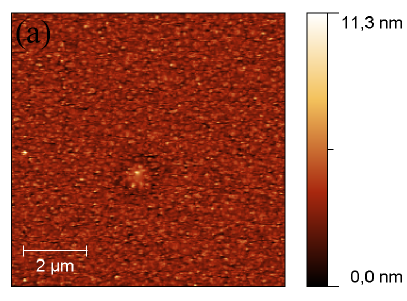
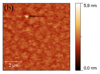
To prepare the junctions, thin films of Ba-122 were used, which were fabricated by pulsed laser deposition (PLD) on a (La,Sr)(Al,Ta)O3 (LSAT) substrate. The films had thicknesses of approximately nm. Details of the deposition process can be found in [12]. To cover the whole sample a gold layer with a thickness of nm was sputtered. The surface showed a good quality with a root mean square (RMS) roughness of less than nm before and after the sputter process (see figure 1). The gold layer forms the barrier between the two superconducting electrodes as well as it avoids possible degradation of the Ba-122 by air, photo resists and other chemicals used in subsequent preparation steps. The thickness of this layer is tunable. For comparison, similar samples prepared with a nm gold layer, show clear Josephson effects [13]. By increasing the thickness of the gold layer up to nm coupling between the superconducting electrodes and thus the critical Josephson current was suppressed. Therefore, samples with thicker barrier layers, more suitable for Andreev reflection studies were chosen in this study.
The Ba-122 base electrode was patterned using photolithography and ion beam etching (IBE) with argon. Optionally, the removed material could be filled by sputtering SiO2, a procedure recommended for thicker films of Ba-122 to avoid cracks in the counter electrode near the edges of the base electrode.
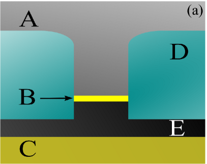
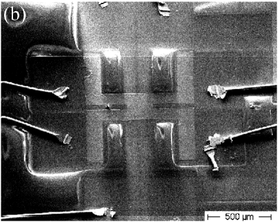
The preparation of the junction areas was performed following described steps. Firstly, we removed the gold and a small area of the Ba-122 layer around the later junction area via IBE. Secondly frameworks of SiO2 with a thickness of were sputtered in order to insulate the electrodes against each other and to define the size of the junction. With our layout we are able to prepare ten junctions with areas between m m and m m on a single sample ( mm mm). Finally, a lead indium (PbIn) alloy was deposited by thermal evaporation for the counter electrode (thickness ). The final structure is shown in figure 2.
Our junction design precisely allows the determination of and for both electrodes separately as well as for the junction itself in four-point geometry. Therefore, it is possible to investigate the temperature dependent electrical properties for each electrode independently and determine their influence on the junction. All eight pads of one junction were contacted via ultrasonic bonding technique with gold wires (diameter m) providing the connection to the measurement equipment.
3 Results and discussion
Characterizing the junction and the electrodes requires information about the differential conductance in dependence of the applied voltage and the differential resistance of the biased current, respectively. For that, a --characteristic was taken for each electrode as well as for the junction and the respective derivation was acquired numerically. The PbIn counter electrode has a critical temperature of K. The differential resistance at K is zero up to a critical current of mA and a critical current density of Acm-2, respectively. For it is independent from the biased current and slightly increases with temperature.

The pure Ba-122 base electrode behaves differently as it is shown in figure 3. The --curve shows hysteretic behavior up to K, which is in contrast to measurements performed on microbridges [14]. At K the critical current is mA, which corresponds to Acm-2. At K the critical current vanishes, which agrees with the of the --curve measured with a bias current of about A. This is in good agreement with the values of the pure Ba-122 thin film [12]. Thus, the preparation process described in section 2 does not influence the properties of the Ba-122. By increasing the temperature the shape of the differential resistance changes. At temperatures above K v-shaped behavior occurs for low currents instead of the u-shaped one at lower temperatures. This nonlinear current dependency will be discussed later in this article. At K the Ba-122 thin film is in the normal state and the resistance reaches a constant value of .
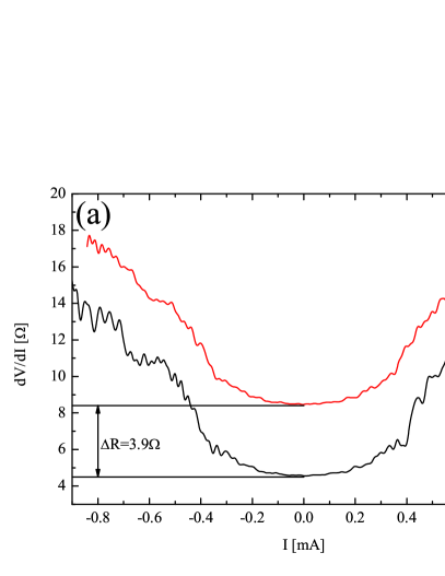
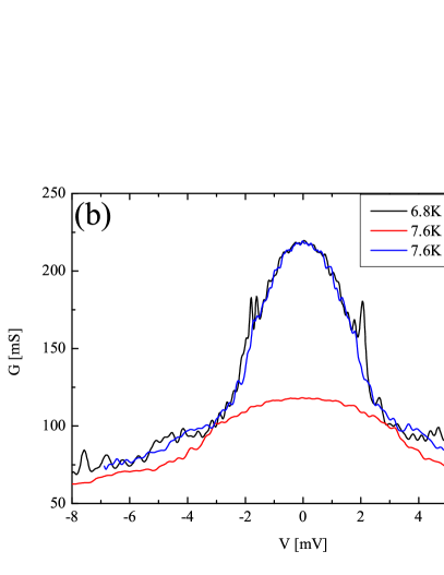
In comparison, the differential resistance of a m m junction is shown for temperatures of K and K, respectively (figure 4(a)). The shape of both curves is very similar, but the differential resistance at K is higher by an offset of about . This is due to the normal state resistance of the PbIn counter electrode, which occurs for K. If the counter electrode switches from superconducting to normal state, the measurement on the junction also switches from a four-point geometry to a three-point one. In this case the resistance of the electrode is in series to the resistance of the junction, and the total measured voltage can be written as sum of the junction voltage and the voltage at the counter electrode. The correct value of the voltage at the junction is then given to be:
It has also to be taken into account that the electrode resistance slightly increases with temperature. The result of this correction is shown in figure 4(b).

For the investigation of junctions, the differential conductance versus voltage is used. Subtraction of the electrode resistance clearly changes the shape of the conductance spectra, so that the curves for K and K look nearly equal. For reducing possible errors in the correction temperatures close to should be examined. This could be challenging due to high noise caused by temperature drift and fluctuation while measuring near .
The Ba-122 base electrode also influences the measured spectra. As shown in figure 5 the nonlinear v-shaped behavior of the electrode, which was mentioned above, can be also seen in the spectra for K. Due to the nonlinear dependence of the electrode resistance one can not, unlike for the counter electrode, derive the junction spectra from the measured one. To describe the conduction spectrum of a single superconductor-normal metal junction one has to use a BTK-model [15] with quasiparticle lifetime extension parameter [16, 17]. A detailed description about the used model and possible extensions for iron-based superconductors (e.g. two-gap superconductivity) is given by Daghero and Gonelli [18].
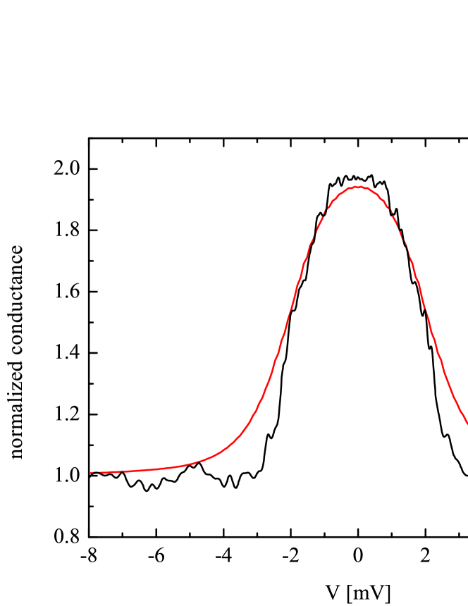
For the junctions presented here a description by the BTK-model is possible for temperatures lower than K as it is shown in figure 6, but despite a general agreement between the model and the measured data larger deviations are found in the range of medium voltages (– meV). The used parameters for this curve were meV, and meV. It can be seen, that the spectrum shows a feature of only a single gap. Also a performed comparison within a two gap model does not lead to a better fit with the measured data. For , the main features of the spectrum are caused by the Ba-122 electrode and not by the junction itself, which prevents a detailed analysis of the energy gap properties near its critical temperature.
4 Summary
To conclude, we developed a layout for SNS’ junctions, which allows us to examine the temperature dependence of both electrodes and a SNS’ junction itself independently from each other. We were able to measure and subsequently correct the influence of the normal state resistance of the PbIn counter electrode on the junction spectrum. Also we showed, that the behavior of the Ba-122 base noticeably influences the junctions spectra for . Finally, we described the conduction spectra of a junction within an extended BTK-model.
References
References
- [1] Seidel P 2011 Supercond. Sci. Technol. 24 043001
- [2] Szabo P, Pribulova Z, Pristas G, Bud’ko SL, Canfield PC and Samuely P 2009 Phys. Rev.B. 79 012503
- [3] Samuely P, Pribulov Z, Szabo P, Prist s G, Bud’ko SL, and Canfield PC 2009 Physica C. 469 507–11
- [4] Lu X et al2010 Supercond. Sci. Technol. 23 054009
- [5] Zhang X et al2010 Phys. Rev.B. 82 020515(R)
- [6] Gorshunov B, Wu D, Voronkov AA, Kallina P, Iida K, Haindl S, Kurth F, Schultz L, Holzapfel B and Dressel M 2010 Phys. Rev.B. 81 060509
- [7] Hardy F, Wolf T, Fisher RA, Eder R, Schweiss P, Adelmann P, v. Löhneysen H and Meingast C 2010 Phys. Rev.B. 81 060501
- [8] Massee F, Huang Y, Huisman R, de Jong S, Goedkoop JB and Golden MS 2009 Phys. Rev.B. 79 220517
- [9] Massee F, Huang YK, Kaas J, van Heumen E, de Jong S, Huisman R, Luigjes H, Goedkoop JB and Golden MS 2010 Euro. Phys. Lett. 92 57012
- [10] Park J, Seunghyun K, Jeon GS, Kim JS, Kim KH and Char K 2011 New J. Phys. 13 033005
- [11] Teague ML, Drayna GK, Lockhart GK, Cheng P, Shen B, Wen HH and Yeh NC 2011 PRL 106 087004
- [12] Iida K, Hänisch J, Thersleff T, Kurth F, Kidszun M, Haindl S, Hühne R, Schultz L and Holzapfel B 2010 Phys. Rev.B. 81 100507
- [13] Schmidt S, Döring S, Schmidl F, Grosse V, Seidel P, Iida K, Kurth F, Haindl S, Mönch I and Holzapfel B 2010 Appl. Phys. Lett. 97 172504
- [14] Rall D, Il’in K, Iida K, Haindl S, Kurth F, Thersleff T, Schultz L, Holzapfel B and Siegel M 2011 Phys. Rev.B. 83 134514
- [15] Blonder GE, Tinkham M and Klapwijk TM 1982 Phys. Rev.B. 25 4515–32
- [16] Dynes RC, Garno JP, Hertel GB and Orlando TP 1984 Phys. Rev. Lett. 53 2437–40
- [17] Plecenik A, Grajcar M, Benacka S, Seidel P and Pfuch A 1994 Phys. Rev.B. 49 10016
- [18] Daghero D and Gonelli RS 2010 Supercond. Sci. Technol. 23 043001