Manipulating optical signals at sub-wavelength scale by planar arrays of metallic nanospheres: Towards plasmonic interference devices
Abstract
We show that interference can be the principle of operation of an all-optical switch and other nanoscale plasmonic interference devices (PIDs). The optical response of two types of planar plasmonic waveguides is studied theoretically: bent chains and Y-shaped configurations of closely-spaced metallic nanospheres. We study symmetric Y-shape arrays as an example of an all-optical switch and demonstrate that effective phase- and amplitude-sensitive control of the output signal can be achieved due to interference effects.
pacs:
78.67.-n 73.20.Mf 85.35.-pSub-wavelength guiding of optical signals is of great interest to information transport and processing. New horizons were opened when linear arrays of metal nanoparticles were introduced as wave guides Quinten98 . It was shown that optical excitations can be channeled into these nanometer scale systems and transmitted over a distance on the order of 1000 nm. Such waveguides are nowadays known as plasmonic arrays. The early work was followed by many other studies of optical guiding at the sub-wavelength scale Brongersma00 ; Hernandez05 ; Waele07 ; Markel07 ; Malyshev08 ; Maier07 . The redirection of optical signals at the nanometer scale is an even greater challenge. To this end, researchers have studied the channeling of surface plasmon polaritons by sub-wavelength V-shaped grooves on a metal surface Pile05 ; Bozhevolnyi05 . Y-splitters, Mach-Zender interferometers, and waveguide-ring resonators have been realized by using bent grooves Bozhevolnyi06 , as well as dielectric-loaded surface plasmon polariton waveguides Holmgaard08 ; Bozhevolnyi08 . Also plasmonic arrays have been considered as Y or T shaped splitters, with the switching induced by the interaction with a nearby molecule Neuhauser07 or the phase and polarization of the light in combination with genetic algorithms Sukharev06 .
In this Letter, we focus on manipulating optical signals at the nanometer scale using two types of planar plasmonic arrays of metallic nanoparticles: bent chains and Y-shaped configurations of identical nanospheres. We show that, in contrast to sharply bent chains, those with a smooth bend can redirect optical signals over an arbitrary angle, up to . The Y-shaped geometry presents two options for controlling the flow of electromagnetic energy: (i) splitting the incoming flux into two or (ii) merging two signals from different branches into one. The efficiency of splitting turns out to be not very high. In the case of the mixer, the relative phase of one (control) signal with respect to the other (input) one allows for interference-induced phase and amplitude control of the output. This opens perspectives for designing nanoscale all-optical switches based on interference phenomena.
The arrays we consider consist of several tens of identical silver nanospheres of radius embedded in a homogeneous dielectric host with a dielectric constant , typical for experiments with silver nanoparticles (see, e.g., Ref. Waele07, ). The center-to-center distance between adjacent nanoparticles is chosen such that , in which case the point dipole approximation for the inter-particle interactions can be used Kelly03 ; Haynes03 ; Yong04 .
To calculate the response of the array to optical fields, we use the quasi-static approximation and characterize the nanospheres by their frequency-dependent polarizability , taken in the form
| (1) |
Here, is the bare polarizability of a single sphere and the next two (-dependent) terms account for the depolarization shift and radiative damping, respectively Meier83 ; stands for the sphere’s radius, while is the wavevector of the exciting light in the host medium. The bare polarizability is expressed as
| (2) |
where the dielectric constant of the metal is taken in the generalized Drude form Waele07
| (3) |
Here, and are, respectively, the bulk metal’s plasma frequency and Ohmic damping constant, while and are adjustable parameters. For silver, , , rad/s, and 1/s Waele07 .
We assume that the sphere at one end of the array (or the two end spheres in the case of the mixer) is excited with a c.w. field of frequency , corresponding to a wave length . We chose the polarization of the exciting field perpendicular to the plane of the array, so that only transverse plasmon modes will be excited in the array. Under steady state conditions, the set of coupled equations for the induced dipole moments of the spheres (labeled by ) reads:
| (4) |
Here, is the incident field at the position of the th dipole and is the retarded Green’s function of the electric field in the dielectric background. For the geometry at hand the latter is given by Weber04
| (5) |
where and . Throughout the paper we consider planar arrays of silver nanospheres with radii of 50 nm and center-to-center distances of 150 nm.
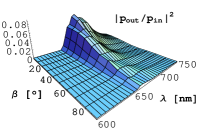

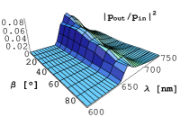
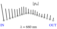
Figure 1 presents our results on redirecting optical signals by bent plasmonic arrays. The top plots correspond to sharp bends, where the chain abruptly changes direction over an angle , while the bottom plots present the case of smooth bends consisting of three spheres (i.e. two spheres lie off the straight lines formed by the input and output legs). In both cases, the chain consists of nanospheres and the leftmost sphere is driven by the incoming field: . To the left is shown the transmittance as a function of and . Clearly, for both cases the maximum transmission occurs around nm; however, for bending angles larger than , the transmission through the smooth bend exceeds by far the one for the sharp bend. This is also seen from the plots to the right, which for both cases show the amplitudes of the dipoles for a bending angle . The explanation is that a smooth bend reduces reflection and radiation losses.
We now turn to Y-shaped arrays. First, we discuss the efficiency of splitting one signal into two. Figure 2 displays our results for a symmetric Y-shaped splitter comprised of seven nanospheres in each branch and with variable aperture angle . The left-most sphere (denoted IN in Fig. 2) is driven by the incoming field, while the output is measured at the end sphere of one of the two other branches (denoted OUT). To the left is displayed the dependence of the transmittance on and . To the right the Y-splitter is shown with the spatial distribution of the , calculated for and the wavelength nm, at which the output is maximum. We see that a reasonable fraction of the signal is transmitted through the branching point; nevertheless, the overall transmission to the output point is low, mostly due to radiative losses.
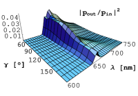
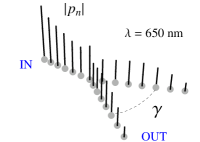
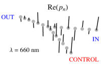
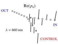
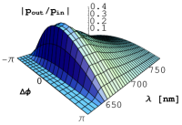
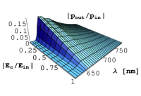
Figure 3 demonstrates all-optical signal control using the Y-shaped plasmonic array described above. Here we excite the extreme spheres of two branches of the array, called IN and CONTROL in the upper panels of Fig. 3 and focus on the output signal at the other end of the mixer. In the top panels we present the spatial distribution of calculated for the case when the input and control signals have the same amplitude and either are in phase (left) or out of phase (right). The calculation was performed for the wavelength at which the output is maximal for the in-phase case. If the phase difference between the input and control signals vanishes, they interfere constructively, resulting in a non-zero output. In the opposite case, , destructive interference leads to zero output. Clearly the output can be controlled by changing . The lower left-hand panel in Fig. 3 presents the overall dependence of the amplitude transmittance on and . For the symmetric mixer considered, as we will show below.
Another way of all-optical control is achieved by keeping the phase difference fixed at , while varying the amplitude of the control field. For this situation, the lower right-hand panel in Fig. 3 shows the amplitude transmittance as a function of and the relative control amplitude . The dependence is linear in , reminiscent of the traditional electronic transistor. When the control amplitude equals the input one, the output signal turns to zero.
Both modes of optical control demonstrated above, phase and amplitude control, follow from the linear nature of the response (superposition), combined with the system’s symmetry. As a result, the signal in the output branch of a symmetric Y-shaped mixer is proportional to . In the case of equal input and control amplitudes, , yielding . On the other hand, for , one gets . These dependencies on and are indeed observed in Fig. 3. Thus, Y-shaped plasmonic waveguides provide for the possibility of either phase- or amplitude-sensitive all-optical control of signals at the sub-wavelength scale. We stress that for a complete cancelation of the input signal by the control one over a wide range of wavelengths, the system should be symmetric note1 .
In conclusion, we studied two types of planar plasmonic waveguides: bent chains and Y-shaped configurations of silver nanospheres. We found that: (i) a smooth bend can redirect optical signals much better than a sharp bend with the same turning angle (ii) Y-shaped arrangements of nanospheres can operate as a splitter of optical signals or as an effective mixer. In the latter case, the output may be controlled by tuning the phase of the control signal relative to that of the input signal. In this regime the system operates as a phase-dependent all-optical switch. Alternatively, the control signal can be kept out of phase relative to the input signal, while tuning its amplitude. In this case the device operates as an optical transistor with a linear control-output characteristic. Finally, we stress that the principles underlying the mixer presented here are very general and also apply to other plasmonic (or radio-frequency) systems. We therefore believe that plasmonic interference devices (PIDs) similar to those considered here, can be fabricated using a wide range of available techniques, such as V-shaped grooves on metal surfaces Bozhevolnyi06 , dielectric-loaded surface plasmon polariton waveguides Holmgaard08 , etc.
This work was supported by NanoNed, a national nanotechnology programme coordinated by the Dutch Ministry of Economic Affairs.
References
- (1) M. Quinten, A. Leitner, J. R. Krenn, and F. R. Aussenegg, ”Electromagnetic energy transport via linear chains of silver nanoparticles”, Opt. Lett. 23, 1331 (1998).
- (2) M. L. Brongersma, J. W. Hartman, and H. A. Atwater, ”Electromagnetic energy transfer and switching in nanoparticle chain arrays below the diffraction limit”, Phys. Rev. B 62, R16356 (2000).
- (3) J. V. Hernández, L. D. Noordan, and F. J. Robicheaux, ”Asymmetric Response in a Line of Optically Driven Metallic Nanospheres”, J. Phys. Chem. B 109, 15808 (2005).
- (4) R. de Waele, A. F. Koenderink, and A. Polman, ”Tunable Nanoscale Localization of Energy on Plasmon Particle Arrays”, Nano Lett. 7, 2004 (2007).
- (5) V. A. Markel and A. K. Sarychev, ”Propagation of surface plasmons in ordered and disordered chains of metal nanospheres”, Phys. Rev. B 75, 085426 (2007).
- (6) A. V. Malyshev, V. A. Malyshev, and J. Knoester, ”Frequency-Controlled Localization of Optical Signals in Graded Plasmonic Chains”, Nano Lett. 8, 2369 (2008).
- (7) S. A. Meier, Plasmonics: Funadamentals and Applications, New York: Springer, 2007.
- (8) D. F. P. Pile and D. K. Gramotnev, ”Plasmonic subwavelength waveguides: next to zero losses at sharp bends”, Opt. Lett. 30, 1186 (2005).
- (9) S. I. Bozhevolnyi, V. S. Volkov, E. Devaux, and T. W. Ebbesen, ”Channel plasmon-polariton guiding by subwavelength metal grooves”, Phys. Rev. Lett. 95, 046802 (2005).
- (10) S. I. Bozhevolnyi, V. S. Volkov, E. Devaux, J. Y. Laluet, and T. W. Ebbesen, ”Channel plasmon subwavelength waveguide components including interferometers and ring resonators”, Nature 440, 508 (2006).
- (11) T. Holmgaardand, Z. Chen, S. I. Bozhevolnyi, L. Markey, A. Dereux, A. V. Krasavin, and A. V. Zayats ”Bend- and splitting loss of dielectric-loaded surface plasmon-polariton waveguides”, Opt. Exp. 16, 13585 (2008).
- (12) Plasmonics Nanoguides and Circuits, ed. S. I. Bozhevolnyi, World Scientific, 2008.
- (13) D. Neuhauser and K. Lopata, ”Molecular nanopolaritonics: Cross manipulation of near-field plasmons and molecules. I. Theory and application to junction control”, J. Chem. Phys. 127, 154715 (2007).
- (14) M. Sukharev and T. Seideman, ”Phase and Polarization Control as a Route to Plasmonic Nanodevices”, Nano Lett. 6, 715 (2006).
- (15) K. L. Kelly, E. Coronado, L. L. Zhao, and G. C. Schatz, ”The Optical Properties of Metal Nanoparticles: The Influence of Size, Shape, and Dielectric Environment”, J. Phys. Chem. B 107, 668 (2003).
- (16) C. L. Haynes, A. D. McFarland, L. Zhao, R. P. Van Duyne, G. C. Schatz, L. Gunnarsson, J. Prikulis, B. Kasemo, M. Käll, ”Nanoparticle Optics: The Importance of the Radiative Dipole Coupling in Two-Dimensional Nanoparticle Arrays”, J. Phys. Chem. B 107, 7337 (2003).
- (17) S. Yong and D. Stroud, ”Surface-plasmon dispersion relations in chains of metallic nanoparticles: An exact quasistatic calculation”, Phys. Rev. B 69, 125418 (2004).
- (18) M. Meier and A. Wokaun, ”Enhanced fields on large metal particles: dynamic depolarization”, Opt. Lett. 8, 581 (1983).
- (19) W. H. Weber and G. W. Ford, ”Propagation of optical excitations by dipolar interactions in metal nanoparticle chains”, Phys. Rev. B 70, 125429 (2004).
- (20) S. A. Maier, M. L. Brongersma, P. G. Kik, S. Meltzer, A. A. G. Requicha, and H. A. Atwater, ”Plasmonics - a route to nanoscale optical devices”, Adv. Mater. 13, 1501 (2001).
- (21) The possibility of such control in the microwave range by T-shaped structures was also discussed in Ref. Maier01 , but no complete cancelation of the output was achieved, due to the lack of symmetry.