Polypropylene Embedded Metal-Mesh Broadband Achromatic Half Wave Plate for Millimeter Wavelengths
Abstract
We describe a novel multi-layered metal mesh achromatic half wave plate for use in astronomical polarimetric instruments. The half wave plate is designed to operate across the frequency range from 125–250 GHz. The wave plate is manufactured from 12-layers of thin film metallic inductive and capacitive grids patterned onto polypropylene sheets, which are then bonded together using a hot pressing technique. Transmission line modelling and 3-D electromagnetic simulations are used to optimize the parameters of the metal-mesh patterns and to evaluate their optical properties. A prototype half wave plate has been fabricated and its performance characterized in a polarizing Fourier transform spectrometer. The device performance is consistent with the modelling although the measured differential phase shift for two orthogonal polarizations is lower than expected. This difference is likely to result from imperfect patterning of individual layers and misalignment of the grids during manufacture.
1 Introduction
A wave plate is an optical component which imparts a differential phase shift to light passing through it in different linear polarization directions. This changes the polarization state of a transmitted wave according to the magnitude of this angular phase difference. A half wave plate (HWP) imparts a 180∘ differential phase shift between light with orthogonal electric field components and can be used to rotate the polarization vector by an angle, by rotating the HWP by an angle with respect to the incident radiation. HWPs are used as polarization modulators in astronomical instruments at millimeter wavelengths ( = 1–3 mm), in particular for measurements of the residual polarization in Cosmic Microwave Background (CMB) anisotropies [1, 2]. These measurements require large spectral bandwidths, cryogenic detectors, and polarimeters with low instrumental polarization and low instrumental emission to ensure photon noise limited detection of the weak polarized CMB anisotropies. This has motivated the development of large area achromatic HWPs [1, 2].
Conventional HWP technologies use birefringent crystalline materials such as Quartz or Sapphire to provide the differential phase delay of orthogonal polarization components. While single crystal plates demonstrate good performance in a narrow frequency band, a broad-band design was reported initially for use at optical wavelengths [3, 4]. This design incorporates 3 or 5 crystal plates of the same thickness, but differentially rotated with respect to the incoming polarized beam to provide a wider range of wavelengths over which the retardation between orthogonal beams is constant. The first achromatic multiple plate HWPs fabricated for a millimeter wave CMB experiment [5] used a sapphire 5-plate design to cover the frequency range from 85–185 GHz [1, 2]. This design has been shown to perform well but is limited in aperture size (290 mm for sapphire [6]) by the availability of materials. Furthermore, the required HWP thickness (17 mm) leads to a small absorption loss (3 %) which becomes a significant source of radiative power and therefore photon noise compared to the 2.73 K CMB, if the HWP is used at 300 K. Lowering the temperature to 100 K eliminates this emission but significantly complicates the instrument design and cost.
To overcome both the limited diameter and the absorption losses in crystalline wave plates, an alternative method of making HWPs based on metal-mesh technology has been proposed [7, 8]. This design uses capacitive and inductive metal-mesh geometries which each generate a frequency dependent phase shift with opposite sign. A first device fabricated from 6 capacitive grids and 6 inductive separated by air/vacuum gaps using accurately etched annular spacers demonstrated a bandwidth of 40 % (60 GHz) with a center frequency of 150 GHz [8]. Here we describe a procedure for optimizing the design of this type of HWP and present measurements of a device fabricated with a new process using dielectric spacers between the metallized sheets fused together with a hot pressing technique to make a solid self-supporting disc [9]. This leads to a robust and easily formed component with small absorption losses and a diameter limited by the available size of the patterned meshes which can be manufactured with diameters 300 mm [10].
In Section 2 of this paper we describe the theory of operation of the HWP and the optimization procedure. We also present the design parameters and expected performance of a HWP optimized for the 125–250 GHz region. In section 3 we describe the device manufacture and in section 4 we present optical performance measurements from its characterization as a HWP using a polarizing FTS.
2 Theory and Modelling
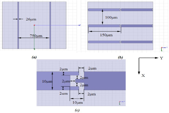
Wave plates based on multiple metal-mesh layers have been built by Lerner [11], Shatrow [7] and Pisano [8]. All of these designs incorporate a combination of two basic types of metal patterns shown in Figure 1. The first pattern consists of continuous parallel metal lines aligned along one polarization axis. A single layer of this pattern acts like an ideal inductive load for incident radiation with electric field polarized parallel to the direction of the lines. The value of the effective inductance depends on the width and spacing of the lines. The second pattern consists of parallel metal lines with small periodically spaced gaps. These lines are aligned along the other polarization axis perpendicular to the first pattern. This pattern acts like a combination of an inductive and a capacitive load in series for incident radiation with the electric field parallel to the direction of these lines. The values of the inductance and capacitance of this pattern also depend on the detailed geometry.
We perform simulations and optimization of this design using two commercially available modelling packages: Advanced Design System (ADS [12]) and High Frequency Structure Simulator (HFSS [13]). We use ADS for transmission line modelling and optimization of a schematic model of the HWP using lumped inductances and capacitances to represent the individual metal layers. Based on the optimized values of the inductances and capacitances determined from ADS, we use HFSS to relate the geometrical parameters of an individual mesh to its lumped impedance by breaking the physical mesh into cells and solving Maxwell’s equations on a cell by cell basis and thus obtaining the scattering matrices for radiation propagation through the mesh.
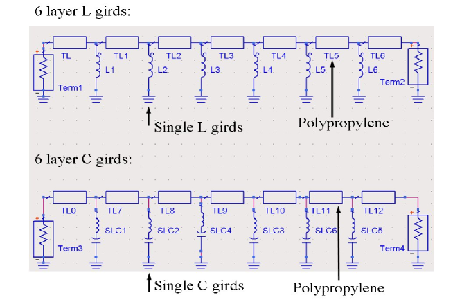
We construct two independent transmission line models in ADS to compute the scattering parameters for the two orthogonal polarizations as shown in Figure 2. The first model considers the transmission of the six aligned inductive grids with appropriate polypropylene dielectric spacers between the grids. The second model considers transmission of the six capacitive grids with polypropylene spacers. For each transmission line model we add an additional section of polypropylene designed to make the total physical thickness of the two transmission line models equal to the sum of the thicknesses of the two sets of six grids and spacers. The scattering parameters from both transmission lines are combined to determine the phase difference between the two polarizations. This is a good approximation to the expected performance of the HWP assuming: i) the grids designed to interact with one polarization do not affect the other polarization and ii) the grids do not generate cross-polarization - i.e the scattering parameters between one transmission line and the other transmission line are assumed to be equal to zero.
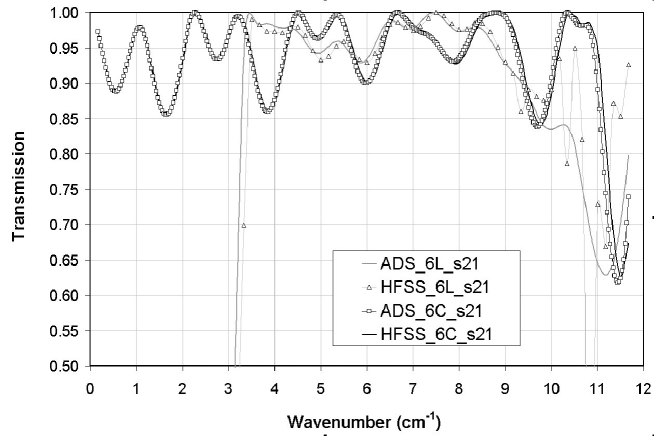
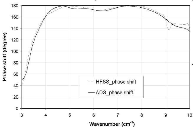
The performance of the HWP schematic is optimized in ADS by varying the values of the inductors and capacitors to achieve a flat phase shift near and to maximize the transmission over the required frequency range from 125 to 250 GHz. This process combines the optimization of the relative phase delay between orthogonal polarizations and a high broad band transmission based on multiple reflections between the metal layers. The optimized transmission for six inductive grids and six capacitive grids are shown in Figures 3 and are seen to both be in excess of 90 % throughout the band. For the prototype discussed here the optimized HWP design gives an overall phase shift between - as shown in Figure 4. Generally, we find that achieving a broad bandwidth requires a high effective capacitance and inductance in the ADS model.
Based on the optimized lumped impedances determined from the schematic model in ADS, we determined the corresponding grid geometries by modelling the scattering parameters of individual metal patterns in HFSS. The geometries of the inductive and capacitive grids are shown in Figure 1. To achieve the high effective lumped capacitance in the optimized ADS design we used a periodic array of metallic planar interdigital capacitor coupled lines as shown in Figure 1. The optimized design also required high inductance which we realised by using very thin planar parallel metallic lines. The frequency-dependent transmission and phase shift for the individual inductive and capacitive grid patterns as determined from ADS and HFSS models are shown in Figures 3 and 4. This indicates that both the parallel inductive wires and the interdigital capacitors are able to be accurately modelled as lumped circuit elements over a wide frequency range. This is not true for distributed resonators used as capacitive elements in the previous air gap HWP design. In addition, the use of non-resonant interdigital capacitors allows the grid dimensions to be scaled independent of the wavelength. Because the spacings between the layers are still designed to be resonant, the overall HWP design is a hybrid between a so-called resonant filter and a metamaterial. The metal strips in the model are simulated as perfect conductors with zero thickness. In practice, the metal layers are 0.4–1 m thick copper. We also perform simulations using an infinitely thin conductor with a sheet resistance corresponding to the measured value (0.05 ).
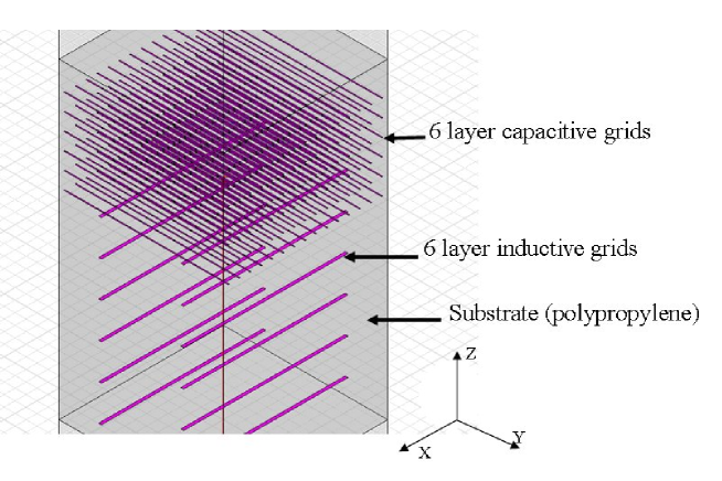
The combined 3-D model of the HWP used for HFSS simulations is shown in Figure 5. The substrate material is polypropylene with dielectric constant of 2.19. The inductive grids only interact effectively with incident radiation polarized with its electric field, , parallel to the strips (E parallel to the x-axis) and the capacitive grids only interact effectively with incident radiation polarized with its electric field, , parallel to the capacitive strips ( parallel to the y-axis). The radiation with E parallel to the y axis is transmitted through the inductive grids with a phase delay due to the optical path length though the dielectric alone. Similarly, the radiation with parallel to the x-axis is transmitted through the capacitive grids with a phase delay due to the optical path length through the dielectric alone. The full design parameters for HFSS models are shown in Table 1.
| Parameter | Value | Units |
|---|---|---|
| Polypropylene thickness above the capacitive layers(Top) | m | |
| Space between the capacitive layers | m | |
| Space between the inductive layers | m | |
| Polypropylene thickness below the inductive layers(bottom) | m | |
| Inductive grids pattern:distance between the lines | m | |
| Inductive grids pattern:line width | m | |
| Capacitive grids pattern:distance between the lines | m | |
| Capacitive grids pattern:line width | m | |
| Inter Digital Capacitor(IDC) pattern (a) | ||
| Capacitive grids pattern:distance between two IDCs | m |
(a) The detailed pattern is shown in Figure 2(c).
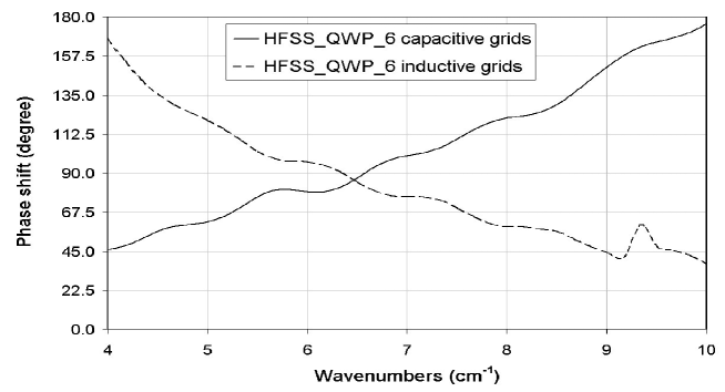
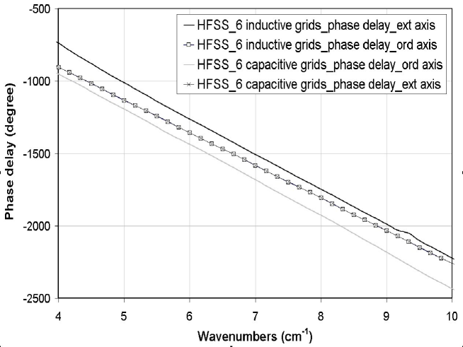
The phase shift is shown in Figure 6 as a function of frequency of the transmitted radiation, compared to the incident radiation through either the combined six capacitive grids embedded in dielectric or the combined six inductive grids embedded in dielectric, calculated from the HFSS model. In both cases, the common phase shift due to the path length through the dielectric substrate has been subtracted. The set of capacitive grids and the set of inductive grids were modelled separately due to the computer memory limit. The overall phase shift of the HWP is the sum of the two phase shifts and is very close to 180 degrees. The phase is frequency dependent so for transmission along the non-reactive axes we expect a linear phase dependence as shown in Figure 7 with respect to the incidence wave. The frequency dependence of the phases for the reactive axes are also shown in Figure 7. The total simulated transmission and phase shift from both ADS and HFSS are compared in Figure 3 and 4. It can be seen that the results from both packages are in very good agreement.
3 HWP manufacture
Fabrication of the prototype HWP plate follows steps used in the manufacturing of far-infrared low-pass filters [14]. In summary, a photolithographic process is used to produce the metal mesh patterns in copper deposited onto thin substrates (8 m polypropylene). The multi-layer structure is then assembled using additional non-metallized dielectric layers to create the appropriate spacing between the elements. It is particularly important to maintain good rotational and translational alignment between the layers as this will affect the final performance. Having assembled all of the meshes, with the inductive and capacitive layers orientated orthogonally to each other, the whole ensemble is then fused by the hot-pressing process used in standard filter production [14].
4 Measurements and data analysis
4.1 Measurements of the prototype HWP
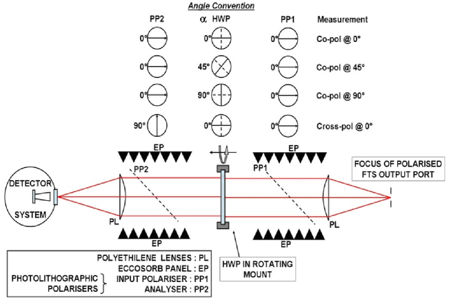
To measure the performance of the final HWP we used a polarizing Fourier Transform Spectrometer (pFTS hereafter). The schematic drawing of the measurement configuration is shown in Figure 8. The pFTS has a natural output focused beam , or more simply a converging beam with angles . To avoid averaging the transmission and phase shift response of the HWP over this range of input angles, a quasi-parallel beam section was created with the use of two planar convex polyethylene lenses. The maximum range of incident angles is then limited by the input source aperture of the pFTS mercury arc lamp source (10 mm), a beam spread of only 1.6∘. Further, the HWP is placed centrally in the collimated beam section between two polarizers placed at a distance such that they can be easily tilted with respect to the optical axis, as shown in Figure 8, to avoid standing wave effects. The efficiency of these polarizers was separately determined to exceed 99.8 % over the range of frequencies of interest (50–1000 GHz) with a cross polarization of less than 0.1 %. The polarizers are initially aligned with respect to each other with the grid wires horizontal and are also aligned with respect to the optical bench in order to avoid any projection effect when tilted.
A first preliminary data set is obtained by scanning the spectrometer in the absence of the HWP, which we will refer to as the background spectrum. This data set is fundamental as it is the set against which all following data sets are divided in order to remove the spectral characteristics of the source, FTS optics and detector system. Subsequently the HWP is inserted in between the tilted polarizers and data is acquired. Each “set” of data consists of an average of 6 spectra each obtained by computing the Fourier transform of an average of 10 interferograms with the mirror scanned in both the forward and backward directions. The processing pipeline uses a non-linear phase correction algorithm [15] and removes any residual asymmetry in the data taken when the mirror is scanned in the forward and backward directions by averaging the two data sets to cancel effects from the finite detector time response.
The bolometric detector was cryogenically filtered to provide spectral coverage from 60 to 660 GHz to minimize photon noise. All data were recorded with a spectral resolution of 1.5 GHz set by the pFTS optical path difference. The transmission spectra are obtained by ratioing the sample spectra against the background spectra to determine the HWP response alone. The HWP rotation was controlled by using a digital angular encoder on a large aperture annular rotator which held the plate.
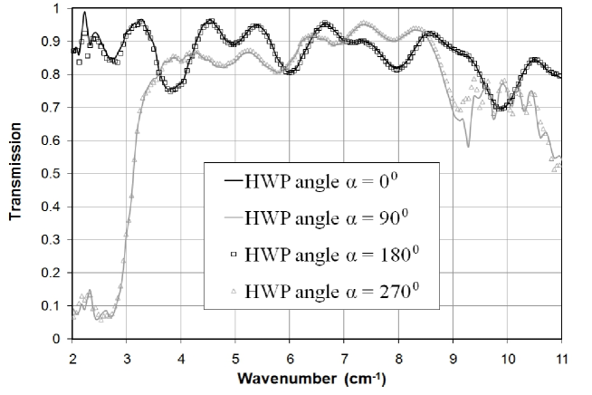
An initial task was to verify that the setup is symmetric with respect to the HWP rotation. To do this, measurements were taken along one axis of the HWP and then repeated after rotation by 180 degrees. Theoretically, due to polarization symmetry, no change should be observed in the pairs of data, as shown in Figure 9 for the two HWP axes. The fact that the curves are superimposed verifies that there are no artifacts arising from a misalignment of the axis of rotation of the HWP rotator with the optical axis of the spectrometer.
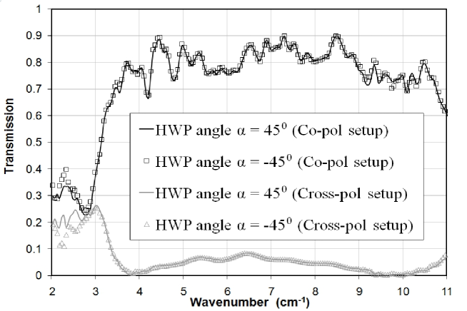
Having identified the polarization axes positions with respect to the mechanical rotator, the HWP was rotated to the null positions of the co-polar setup (Figure 8) and measured in both the co-polar and cross-polar response at +45 and -45 degrees again verifying that there were no measurable systematic effects. Unlike the co-polarization maxima where symmetry is effectively broken by the incoming polarization either being parallel to the inductive or the capacitive grids, all the null degree positions are expected to perform in an identical manner. This is indeed the case as can be seen from the data in Figure 10. The curves are again superimposed in pairs to show that the symmetry of the phase shift is preserved and that the two sets of capacitive and inductive grids are perpendicularly aligned with good precision.
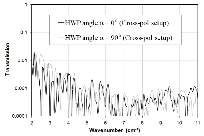
The cross-pol transmission on axis (0 and 90 degrees) is shown in Figure 11. Similarly to a single crystal plate cut along its principal axis, there should be no polarization rotation. The fact that the transmission here is less than 0.1 % (corresponding to the noise level) points to a good alignment of all the grids in the prototype.
4.2 Discussion of HWP performance
The average transmissions for linear polarization along the two axes of the HWP assembly are between 86 and 91 percent, the precise value being determined by the spectral range that is considered within the [105,315] GHz interval where the phase shift is the most effective. These transmissions, shown in Figure 12, match closely the HFSS simulations up to (300 GHz) where diffraction starts.
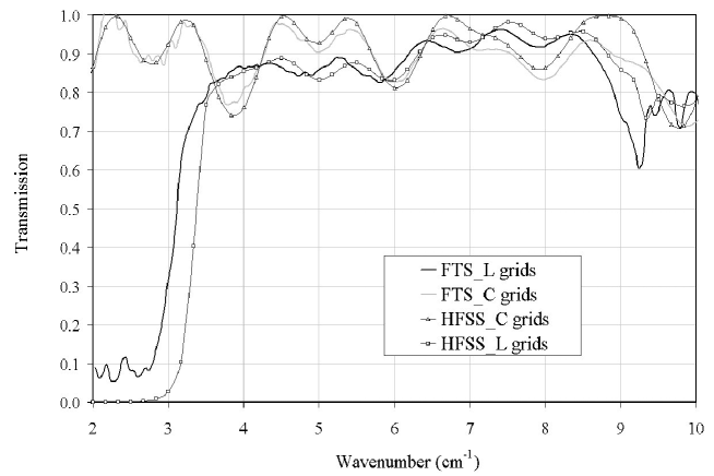
The simulation includes measurements of the absorption loss in the polypropylene substrate material [14] and a resistivity for copper which is increased to represent an evaporated rather than bulk material. The fit to the data is seen to be good for the capacitive axes as shown by the overlay in Figure 12, but not so good for the inductive axis. We believe that the poor fit here has several origins. First the inductive strips could be slightly over-etched in the manufacture process which would lead to the low frequency edge moving to shorter frequencies as observed. Secondly, the copper thickness of 0.1 m is equivalent to the skin depth near 1 cm-1 which could explain the non-zero rejection at low frequencies and associated phase errors. Finally, there could be systematic effects arising from the non-perfect alignment of the inductive and capacitive elements during manufacture, producing an additional source of reflection (due to impedance mismatch). Currently HFSS cannot cope with large open structures for which the symmetry is broken. However, the fact that this prototype HWP is seen to perform well shows that these systematic effects are small.
One of the key points of polarization modulation is the leakage between axes. To be effective, the phase delay between the two HWP axes should be as close to as possible to avoid transforming linear polarization in elliptical, hence losing efficiency when used as a linear polarization modulators. The phase cannot be directly measured in a pFTS but it can be indirectly inferred from the expected value of the Mueller Matrix of the optical element.
The Mueller matrix of a phase-delaying device with non-identical axes transmission can be written in its most simple form, when the reference frame is aligned with the plate axes, as:
| (1) |
We have used the notation presented in [16] where and represent the intensity transmissions on the plate’s two axes and is the phase shift between the two axes. Here we are interested in extracting the frequency dependence of these three quantities from the spectral measurements.
Recovering the first two parameters is intuitively straightforward by aligning the input and output polarizers and measuring the plates’ spectral transmission. Extracting the phase requires a combination of measurements. First consider the Mueller matrix of the HWP rotated by 45 degrees:
| (2) |
This allows measurements performed with Stokes vectors Q to extract a dependence on the phase. By noting a set of data taken with the HWP at an angle between parallel polarizers (Co-pol in Figure. 8) as we can combine the sets of measurements in the following way to obtain the phase shift as shown in Figure 13:
| (3) | |||
| (4) |
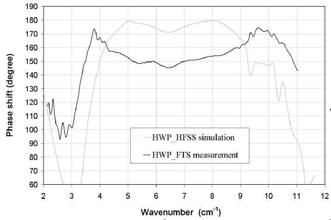
The resulting phase shift presents a similar functional dependence but is also substantially different quantitatively from the HFSS simulated value. The discrepancy between expected and measured phase shift is likely to be sought in the physical parameters that cannot be easily introduced in the HFSS simulation due to resulting excessively large mesh geometries. One of these parameters is the thickness of the copper deposition on the metal mesh layers. A copper thickness of one hundred nanometers is of the same order of the skin depth of the metal at the frequencies of interest. As the skin depth scales as , the additional phase delay produced by delayed currents induced on the other side of the metal meshes will vary with frequency across the band. A crude estimation of the absorption can be obtained by considering the envelope of the parallel polarizer transmission curves as a smooth and monotonic function of frequency. This shows that an overall absorption of 3 to 5 percent can be expected from the combined absorption of the polypropylene substrate and the loss due to the imperfect conductivity of the metal.
5 Conclusions
It is important to put the performance of this HWP into context with the current crystalline HWPs. The two represent very different technologies and both have manufacture and performance issues. Here we attempt to summarize these differences to aid in their selection for future instruments.
Although the prototype has been designed and built at mm-wavelengths, its broadband nature and impedance characteristics are conserved when scaling the geometries to operate at higher frequencies (at sub-mm wavelengths and frequencies higher than 1 THz), where crystalline absorption is indeed a problem. A return loss of about ten percent is experienced for this prototype metal mesh HWP without applying additional anti-reflection coating; its average transmission is an improvement with respect to most crystalline birefringent waveplates which have a large impedance mismatch due to the high index of refraction of the crystal material. Single layer anti-reflection coatings, while improving the insertion loss of the crystal alternatives, cannot avoid the inherent crystalline absorption, which gets progressively worse at higher frequencies [17]. While reflections can present a problem due to ghost images appearing in a polarimeter system which has more than one reflecting element, absorption is a more serious problem for low background sub-mm astronomical instruments, since the detectors employed in these are background photon noise limited. Thermal grey body emission from a room temperature HWP, which for low loss is proportional to its absorption, can present a significant additional noise component. Most experiments are thus forced to position the HWP modulator inside the cryogenic housing at temperatures below 100K, since the absorption decreases and the grey body emission is also reduced.
While cryogenic deployment of the hot-pressed sample in question, which is unnecessary, would not constitute a problem, in the case of AR coated crystals large temperature gradients require great attention and planning in both the construction process and in the mount design.
Although the recovered phase is not an improvement on existing achromatic crystalline devices [1, 16], the modulation efficiency of the HWP is always above 85 % in a 90 % spectral bandwidth with the best performance above 96 % modulation efficiency in two 10 % narrow bands (centered at 125 and 295 GHz) at the extremes of its spectral range.
In conclusion we note that overall there are numerous instrumental advantages of this device that make it a competitive alternative to crystalline HWP, especially at higher frequencies and where wide spectral bandwidth is required.
References
- [1] Savini G., Pisano G., Ade P.A.R.., “Achromatic Half-wave Plate for Submillimeter Instruments in Cosmic Microwave Background Astronomy: Modeling and Simulation”, Applied Optics, Vol. 45, No. 35, December 10, 2006.
- [2] Pisano G., Savini G., Ade P.A.R., “Achromatic Half-wave Plate for Submillimeter Instruments in Cosmic Microwave Background Astronomy: Experimental Characterization”, Applied Optics, Vol. 45, No. 27, September 20, 2006.
- [3] Pancharatnam S., “Achromatic Combinations of Birefringent Plates”, Raman Research Institute, Bangalore, Memoir 71, pp. 137–144, 1955.
- [4] Title A.M. and Rosenberg W.J., “Achromatic Retardation Plates”, In Polarizers and Applications, SPIE Proceedings Vol. 307, Edited by Giorgio B. Trapani, Bellingham, WA: Society for Photo-Optical Instrumentation Engineers, 1981. pp. 120–131, 1981.
- [5] Ade P., Bock J., Bowden M., Brown M.L., Cahill G.,etc., “First Season QUaD Temperature and Polarization Power Spectra”, Astrophysics Journal 674, pp. 22–28, 2008.
- [6] Matsumura T., Hanany S., Ade. P.A.R., Johnson B.R., Jones T.J., Jonnalagadda P., and Savini G., “Performance of Three- and Five-Stack Achromatic Half-Wave Plates At Millimeter Wavelengths”, Applied Optics, Vol. 48, Issue 19, pp. 3614–3625, 2009.
- [7] Shatrow A.D., Chuprin A.D., Sivov A.N., “Constructing The Phase Converters Consisting of Arbitrary Number Oftranslucent Surfaces”, IEEE Transactions on Antenna and Propagation, Vol. 43, No. 1, pp. 109–113, January 1995.
- [8] Pisano G., Savini G., Ade P.A.R., and Haynes V., “Metal-Mesh Achromatic Half-wave Plate for Use at Submillimeter Wavelengths”, Applied Optics, Vol. 47, No. 33, 2008.
- [9] Zhang, J; Ade, P A R; Mauskopf, P; Moncelsi, L; Savini, G; Whitehouse, N., “New Artificial Dielectric Metamaterial and Its Application As A Terahertz Antireflection Coating”, Applied Optics, Vol. 48 Issue 35, pp. 6635–6642, 2009.
- [10] Ade, P.A.R., Pisano G., Tucker, C., and Weaver S., “A review of Metal Mesh Filters”, Millimeter and Submillimeter Detectors and Instrumentation for Astronomy III, Proceedings of the SPIE, Vol. 6275, pp. 62750U, 2006.
- [11] Lerner, D.S., “A Wave Polarization Converter for Circular Polarization”, IEEE Transactions on Antennas Propagation, Vol. 13, No. 1, January 3-7, 1965.
- [12] Agilent website for ADS: http://www.home.agilent.com/agilent/home.jspx/.
- [13] Ansoft HFSS website: http://www.ansoft.com/products/hf/hfss/.
- [14] Tucker C. and Ade P.A.R., “Metal-Mesh Filters for THz Applications”. Infrared and Millimeter Waves, 2007 and the 2007 15th International Conference on Terahertz Electronics, IRMMW-THz Joint 32nd International Conference, pp. 973–975, 2007.
- [15] Forman M.L., “Fast Fourier-Transform Technique and Its Application to Fourier Spectroscopy”, JOSA, Vol. 56, Issue 7, pp. 978–979, 1966.
- [16] Savini G., Ade P.A.R., House J., Pisano G., Haynes V., and Bastien P., “Recovering The Frequency Dependent Modulation Function of The Achromatic Half-Wave Plate for POL-2: The SCUBA-2 Polarimeter”, Applied Optics, Vol. 48, pp. 2006–2013, 2009.
- [17] Lau J., Fowler J., Marriage T., Page L., Leong J., Wishnow E., Henry R., Wollack E., Halpern M., Marsden D., and Marsden G., “Millimeter-wave Antireflection Coating for Cryogenic Silicon Lenses”, Applied Optics, Vol. 45, No. 16, pp. 3746–3751, 1 June 2006.