Silicon spin communication
Abstract
Recent experimental breakthroughs have demonstrated that the electron spin in silicon can be reliably injected and detected as well as transferred over distances exceeding 1 mm. We propose an on-chip communication paradigm which is based on modulating spin polarization of a constant current in silicon wires. We provide figures of merit for this scheme by studying spin relaxation and drift-diffusion models in silicon.
Virtually all modern information technologies are based on modulating electromagnetic waves whose propagation is described by Maxwell equations. When this technique is used for on-chip communication, signals are transmitted via metallic wires, modeled as transmission lines with the voltage and current being distance and time-dependent. The main drawbacks of this technique relate to dynamical crosstalk between wires, RC bottlenecks, and electromigration between silicon and its interconnect material.ITRS ; Deutsch1998:PIEEE These effects become increasingly acute with reducing the spacing between adjacent wires and with increasing the modulation frequency. Implementing new high-performance communication schemes and interconnects is thus central to the scaling of integrated circuit technologies.
We propose a different concept for data communications which relies on the modulation of the electrons’ spin polarization of a constant current in Si wires. If spin, rather than voltage, encodes information, then the wires remain charged indefinitely where the constant charge current is used to drive the information but not to carry it. This scheme is free of dynamical transmission line effects, electromigration problems and the need for wire shielding. Using the electron spin to processDery2007:N ; Dery2011:IEEE or transfer information in semiconductors may spur spintronic applications beyond information storage.Zutic2004:RMP ; Maekaea_Book
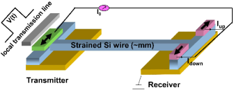
Silicon is a promising material candidate due to its weak spin-orbit coupling.Zutic2006:PRL ; Cheng2010:PRL ; Li2010:PRL ; Li2011:P Measured spin lifetime of intrinsic Si at low temperatures is within the s range,Huang_PRL07 and 10 ns at 300 K,Lancaster_PPSL64 ; Lepine_PRB70 the longest of any inorganic bulk semiconductor. At the saturation drift velocity of silicon (107 cm/s), this corresponds to a transport length scale exceeding 1 mm. Furthermore, recent advances in spin injection into Si Appelbaum2007:N ; Jonker2007:NP ; Dash2009:N ; Ando2010:APL ; Suzuki2011:APE ; Li_nature_com11 are encouraging for experimental implementation of spin interconnects. Figure 1 shows a scheme of the spin-based communication protocol. The transmitter generates information via modulation of the magnetization in the upper spin-injector contact. This is realized by modulating the voltage of a short and local transmission line above the contact. The current, , across the ferromagnet/Si interface is constant and driven by an external source. is comprised primarily of electrons whose spin matches the spin-up population of the injector contact. This constant current flows in the Si wire without interfering with the information that may propagate in the adjacent wires (not shown). At the receiver, is split into two paths where electrons prefer to be extracted from a ferromagnetic contact whose magnetization direction matches their own spin direction. Thus, the current in one of the receiver’s contacts is greater than in the other contact and a local differential device/amplifier may resolve the encoded information.
The spin relaxation time and mobility in the Si wire are the most important parameters in setting the proposed on-chip communication lengthscale. We consider non-degenerate Si wires with cross section areas larger than 1010 nm2. Since the effective electron Bohr radius and the mean free path of thermal electrons in Si at 300 K is of the order of a few nm, the transport in such wires is bulk-like and the spin relaxation is governed by Elliott-Yafet processes. Elliott_PR54 ; Yafet_1963 Taking into account the six conduction band valleys in silicon, we follow the classical categorization into intravalley and intervalley scattering where the latter has contributions from and processes which denote, respectively, scattering between opposite valleys and between valleys on different crystal axes.Cardona_Book
We first study how can be tailored using strain and then we incorporate our findings into a spin dependent drift-diffusion description of the wire.Zutic2004:RMP ; Maekaea_Book The strain has two effects which increase . The first is to lift the energy degeneracy between valleys that reside on different axes (valley splitting) which suppresses the -process contribution to spin-relaxation. Tang2011:P ; Cheng2010:PRL In an unstrained Si this contribution is dominant at high-temperatures.Li2011:P Valley splitting is possible if the diagonal strain components are not equal (e.g., via [001] and [011] stress configurations). The second effect is to increase the energy spacing between the bottom of the conduction band and the spin hot-spot at the edge of the Brillouin zone.Li2011:P ; Cheng2010:PRL Spin hot-spots give rise to fast spin relaxation due to the enhanced spin-mixing of states in these regions.Fabian_PRL98 Application of strain with nonzero off-diagonal components (e.g., via [111] and [011] stress configurations) can transfer the two-band degeneracy from the X-point region to farther energy regions in the Brillouin zone. A comprehensive examination of the strain effects will be studied elsewhere. Here we summarize the results that are most relevant to the spin communication protocol.
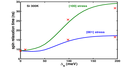
Figure 2 shows simulation for the spin relaxation suppression in Si as a function of stress levels along the [001] and [100] crystal axes. These simulations follow a numerical procedure similar to the unstrained case.Cheng2010:PRL Strain effects were incorporated into the band structure calculation following Ref. [Rieger_PRB, ] and into the phonon dispersion and polarization vectors following Ref. [Eyrigit_PRB96, ]. The figure shows that at 300 K can be four times longer than the unstrained case. This optimal improvement is reached when the spin quantization axis (chosen parallel to the [001] crystal axis) is perpendicular to the axis of valleys with lower energy. The saturation of at higher stress levels is reached when -processes are effectively quenched and the dominant contribution to spin relaxation comes from intravalley scattering,
| (1) |
where and are unit vectors along the stress and spin quantization axes, respectively. , and denote, respectively, components of spin relaxation in the unstrained case due to intravalley, -process and -process scattering. Their analytical forms are given in Ref. Li2011:P, .
Our findings are considerably more conservative than those of Tang et al. who predicted an order of magnitude longer when the -processes are quenched.Tang2011:P The reason for the discrepancy is that in our case the intravalley rate due to scattering with acoustic phonons is much faster, 10 s at 50 K and ns at 300 K, consistent with Larmor precession and spin-valve measurements of spin injection in Si,Huang_PRL07 ; Appelbaum2007:N ; Huang_PRB10 with previous detailed numerical calculation,Cheng2010:PRL and with analytical formalism.Li2011:P It is possible that the coupling between the upper and lower conduction bands which provides the dominant contribution to intravalley spin relaxation,Li2011:P is not included in the model in Ref. [Tang2011:P, ].
To explore the feasibility of the proposed communication scheme, we model spin-dependent pulse propagation in a strained Si wire. Using a drift-diffusion model, the propagation of a pulse is,
| (2) |
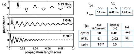
where denotes the current spin polarization at location and time , is the polarization at the transmitter, is the diffusion constant, and is the electric field. Using the room temperature parameters of strained Si, =35 ns from Fig. 2 and =2500 cm2/Vs,Ungersboeck_IEEE07 we model propagation of a (spin) pulse train across a strained Si wire. Figure 3(a) shows a snapshot of the current polarity along the 1 mm wire due to transmission of a pulse train at three different repetition rates. The drift velocity is =4106 cm/sec. We consider the ‘worst case scenario’ in which the polarity is flipped with each pulse. After 1 mm propagation the current remains spin-polarized at 1 GHz pulse repetition rate where the peak polarity drops by an order of magnitude (from to 0.1).
To provide figures of merit of this technique, we define the maximal repetition rate, , which is mostly dictated by the intermixing of nearby spin-pulses (diffusion effect). If we limit the intermixing to 10% then,
| (3) |
where is the voltage drop across the wire and is the thermal voltage, is the latency (propagation delay) and is the maximal propagation length limited by spin relaxation (). Using the previous and parameters, the table in Fig. 3(b) shows the maximal propagation lengths of the communication scheme. Figure 3(c) shows a scheme of a lateral circuit whose interconnects are strained silicon wires with the parameters on the right hand side of the figure. Assuming a 50% areal filling with wires, the attainable bandwidth for such a lateral circuit working at 5 V and 0.13 GHz is 1300 Tbit/(scm2) and the needed power is 0.25 Watt (Joule heating of the wires). These bandwidth and power are by far superior to any other existing technique (see, e.g., Fig. 3 in Ref. [McFadden_AO06, ]). On the other hand, the main drawback of the proposed communication scheme is the increased latency (10 ns per 1 mm compared with 10-20 ps in metallic transmission lines and optics on-chip). Nonetheless, the extremely high bandwidth of spin interconnects may satisfy wiring demands between nearest neighbor nodes of practical multi-core microprocessor architectures and they may also spur communication schemes in emerging 3D electronic technologies, reconfigurable logic and optoelectronic systems (e.g.; in spin-lasers by modulating the information via the polarization rather than the amplitude of lightLee2010:APL ; Holub2007:PRL ; Rudolph2003:APL ).
In conclusion, we have studied the performance of spin interconnects implemented in silicon wires. By using strain, the propagation distances are predicted to reach the 1 mm scale at room temperature while keeping a high fidelity of the signal, demonstrating the feasibility of high-performance spin interconnects. We have also provided figures of merit for the maximal spin-pulse repetition rate and propagation length as well as discussing the latency versus bandwidth trade-offs.
This work was supported by the AFOSR-DCT FA9550-09-1-0493, NSF-ECCS 0824075, NSF-ECCS CAREER 054782, and U.S. ONR N0000140610123.
References
- (1) 2009 International Technology Roadmap for Semiconductors www.itrs.net
- (2) A. D. Deutsch, Proc. IEEE 86, 315 (1998).
- (3) H. Dery, P. Dalal, L. Cywinski, and L. J. Sham, Nature 447, 573 (2007);
- (4) H. Dery, H. Wu, B. Ciftcioglu, M. Huang, Y. Song, R. Kawakami, J. Shi, I. Krivorotov, I. Žutić, L. J. Sham, arXiv:1101.1497, preprint.
- (5) I. Žutić, J. Fabian, and S. Das Sarma, Rev. Mod. Phys. 76, 323 (2004); J. Fabian, A. Mathos-Abiague, C. Ertler, P. Stano, and I. Žutić, Acta Phys. Slov. 57, 565 (2007).
- (6) S. Maekawa, Concepts in Spin Electronics, (Oxford, New-York, 2006).
- (7) I. Žutić, J. Fabian, and S. C. Erwin, Phys. Rev. Lett. 97, 026602 (2006).
- (8) J. L. Cheng, M. W. Wu and J. Fabian, Phys. Rev. Lett. 104, 016601 (2010).
- (9) P. Li and H. Dery, Phys. Rev. Lett. 105, 037204 (2010).
- (10) P. Li and H. Dery, arXiv:1103.3800, preprint.
- (11) B. Huang, D. J. Monsma, and I. Appelbaum, Phys. Rev. Lett. 99, 177209 (2007); B. Huang, H.-J. Jang, and I. Appelbaum, Appl. Phys. Lett. 93, 162508 (2008);
- (12) G. Lancaster, J. A. Van Wyk, and E. E. Schneider, Proc. Phys. Soc. London 84, 19 (1964).
- (13) D. J. Lépine, Phys. Rev. B 2, 2429 (1970).
- (14) I. Appelbaum, B. Q. Huang, and D. J. Monsma, Nature 447, 295 (2007).
- (15) B. T. Jonker, G. Kioseoglou, A. T. Hanbicki, C. H. Li, and P. E. Thompson, Nature Phys. 3, 542 (2007).
- (16) S. P. Dash, S. Sharma, R. S. Patel, M. P. de Jong, and R. Jansen, Nature 462, 491 (2009).
- (17) Y. Ando, K. Hamaya, K. Kasahara, Y. Kishi, K. Ueda, K. Sawano, T. Sadoh, and M. Miya, Appl. Phys. Lett. 94, 182105 (2009).
- (18) T. Suzuki, T. Sasaki, T. Oikawa, M. Shiraishi, Y. Suzuki, and K. Noguchi, App. Phys. Express 4, 023003 (2011).
- (19) C. H. Li, O. M. J. van ’t Erve, and B. T. Jonker, Nature Communications 2, 245 (2011).
- (20) R. J. Elliott, Phys. Rev. 96, 266 (1954).
- (21) Y. Yafet, in Solid State Physics, edited by F. Seitz and D. Turnbull (Academic, New York, 1963), Vol. 14, p. 1.
- (22) P. Y. Yu and M. Cardona, Fundamentals of Semiconductors (Springer, Berlin, 2005), 3rd Ed., Ch. 2-5.
- (23) J.-M. Tang, B. T. Collins, and M. E. Flatté, arXiv:1104.9705, preprint.
- (24) J. Fabian and S. Das Sarma, Phys. Rev. Lett. 81, 5624 (1998).
- (25) M. M. Rieger and P. Vogl, Phys. Rev. B 48, 14276 (1993).
- (26) by R. Eyriğit and I. R. Herman, Phys. Rev. B 53, 7775 (1996).
- (27) Heterostructures with large internal strain are undesirable since the stressed layer cannot be grown beyond a few nm without strain relaxation (e.g. in Si1-xGex/Si with ). Accordingly, in such confined structures one should also consider spin relaxation due to interfacial scattering and structural inversion asymmetry.
- (28) B. Huang and I. Appelbaum, Phys. Rev. B 82, 241202(R) (2010).
- (29) E. Ungersboeck, S. Dhar, G. Karlowatz, V. Sverdlov, H. Kosina, and S. Selberherr, IEEE Trans. Electron Device 54, 2183 (2007).
- (30) M. J. McFadden, M. Iqbal, T. Dillon, R. Nair, T. Gu, D. W. Prather, and M. W. Haney, Appl. Opt. 45, 6358 (2006).
- (31) J. Lee, W. Falls, R. Oszwałdowski, and I. Žutić, Appl. Phys. Lett. 97, 041116 (2010).
- (32) M. Holub, J. Shin, D. Saha, and P. Bhattacharya, Phys. Rev. Lett. 98, 146603 (2007).
- (33) J. Rudolph, D. Hägele, H. M. Gibbs, G. Khitrova, and M. Oestreich, Appl. Phys. Lett. 82, 4516 (2003).