Graphene microwave transistors on sapphire substrates
Abstract
We have developed metal-oxide graphene field-effect transistors (MOGFETs) on sapphire substrates working at microwave frequencies. For monolayers, we obtain a transit frequency up to 80 GHz for a gate length of 200 nm, and a power gain maximum frequency of about 3 GHz for this specific sample. Given the strongly reduced charge noise for nanostructures on sapphire, the high stability and high performance of this material at low temperature, our MOGFETs on sapphire are well suited for a cryogenic broadband low-noise amplifier.
Graphene is a two-dimensional system with high carrier mobility that provides a rich playground for building novel high-frequency devices schwiertz2010 . Although the characterization of graphene’s electronic properties is one of the most active fields in condensed matter physics, most experiments focus on its dc properties.
Metal-oxide graphene field-effect transistors (MOGFETs) operating in the microwave range have already been realized meric2008 ; lin2009 ; moon2009 ; lin2009a ; farmer2009 ; lin2010a ; lin2010 ; dimitrakopoulos2010 ; liao2010 ; lee2010 ; wu2011 ; meng2011 . First microwave measurements on MOGFETs yielded transit frequencies of GHz at 500-nm gate length meric2008 . These very promising results were later optimized further by reducing the gate length lin2009 ; lin2010a ; lin2010 ; wu2011 and using different techniques to grow the top-gate oxide layer farmer2009 . Transit frequencies of 100 GHz have been reported for wafer-scale MOGFETs produced with graphene obtained by graphitization of SiC lin2010 ; dimitrakopoulos2010 . Values up to 155 GHz for a 40-nm gate length with an almost temperature independent gain wu2011 have been demonstated using MOGFETs fabricated with CVD-grown graphene lee2010 ; wu2011 . Very recently transit frequencies up to 300 GHz have been reported using a Co2Si nanowire as gate liao2010 . Despite the lack of an energy gap making graphene unsuitable for logic applications, these results are very promising for the use of MOGFETs as microwave low-noise amplifiers. Still, graphene has yet to show its full potential and the ”terahertz gap” remains to be bridged schwiertz2010 .
Reducing the gate length and the contact resistance, improving the carrier mobility and limiting parasitic capacitances should further improve the high-frequency performance of MOGFETs schwiertz2010 ; thiele2010 ; pince2010 ; liao2010a . Here, we present microwave measurements of MOGFET devices fabricated on sapphire substrates. We find transit frequencies up to 80 GHz for a gate length of 200 nm. The use of such a fully insulating substrate allows to minimize losses and parasitic capacitances arising from finite conduction of the substrate, which is present even in intrinsic semiconductors. Charge noise is minimized on sapphire, which is therefore used as a substrate for microwave devices such as detectors and qubits. Moreover, because of the high energy of polar optical phonons in sapphire, the substrate-limited mobility for graphene is expected to be higher than on oxidized silicon. Given the high thermal conductivity of sapphire, the very high cut-off frequency and the low impedance of the MOGFET, our device could be integrated in a monolithic microwave integrated circuit (MMIC) such as ultra-high bandwidth amplifiers.

Graphene flakes were prepared using Scotch tape micromechanical cleavage on natural graphite, and deposited on 330 m thick C-plane sapphire substrate. The graphene sheets were located using optical microscopy and characterized by Raman spectroscopy. Fig. 1(a) shows the Raman spectrum of the monolayer graphene flake on sapphire used for sample . The samples were prepared by e-beam lithography. To avoid charging effects of the insulating substrate we used a layer of standard PMMA resist plus a second layer of water-soluble conducting polymer (Espacer 300Z from Showa Denko K.K.). The contacts were realized by evaporating a Ti(10 nm)/Al(120 nm) bilayer. A 25-nm Al2O3 gate insulator was prepared by atomic layer deposition as described by Kim et al. kim2009 . The dielectric constant of our oxide is estimated to . A second lithography step allowed the patterning of the top gates followed by a Ti(10 nm)/Al(100 nm) bilayer deposition. We chose a geometry of a coplanar wave guide with double-gate structure as shown in Fig. 1(b). The measurements were performed at room and low temperatures (77 K) on RF probe stations. The voltage biases (both drain-source voltage and gate voltage ) were applied using a voltage source and bias-tees (see Fig. 1(c)). The drain-source current was deduced from the voltage drop across the bias resistor . The scattering parameters were measured with a two-port vector network analyzer (VNA Anritsu 37369C) calibrated using a short-open-load-thru calibration. In order to extract the intrinsic transit frequency of the transistor, we applied a de-embedding procedure by subtracting the signal of an open and short structure strictly similar to the measured MOGFET using the relation: , where is the admittance calculated from the measured scattering parameters using conventional two-port network analysis pozar . This technique has proven to be useful to probe diffusion in graphene pallecchi2011 . We will present measurements of device , which showed the best performance in our batch of 10 samples. The double-gate device has a 200 nm gate length, 800 nm and 3.7 m channel length and width respectively. From geometrical considerations, we estimate the total gate capacitance of the double-gate device fF.
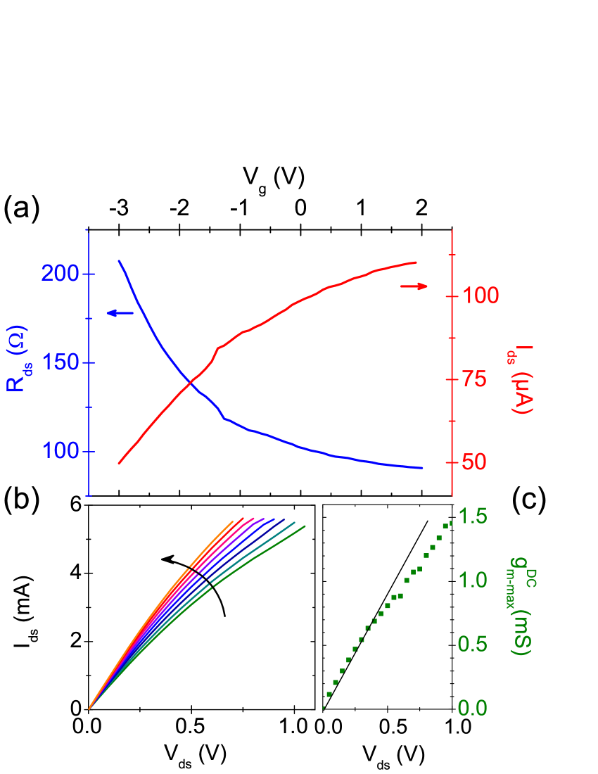
First we characterize the sample’s dc properties to define the parameter range where the transconductance is maximum. Fig. 2(a) shows both the resistance and the drain-source current as a function of gate voltage . The resistance was extracted from the curves at relatively low bias ( = 10 mV). Note the low impedance of the device which is of great advantage for integration in microwave circuits. We observed that in all the samples the graphene sheet is naturally n-doped, as expected for aluminum contacts. The Dirac point could not be reached within our gate-voltage range. Accordingly, the transconductance does not saturate but reaches a still considerable value mS/mV. Fig. 2(b) displays curves of the MOGFET for several gate voltages becoming non-linear at large bias. We observe a tendency to saturate, but despite the large current passing through the device a full saturation is not found, as typically observed in graphene field-effect transistors meric2008a ; bachtold . Fig. 2(c) shows the maximum transconductance versus , which deviates from linear behavior as the curves become non-ohmic.

We now discuss the RF properties of our MOGFET. The short-circuit current gain defined as is calculated from the scattering parameters using the common-source small-signal equivalent circuit model pozar . In Fig. 3(a), the high-frequency transconductance corresponding to the real part of the admittance is displayed as a function of for V. As expected for a diffusive transistor the increases linearly with at low bias and then starts to saturate. We find a maximum transconductance 0.25 mSmV at V and V. According to the definition of the current gain, the transit frequency corresponds to the frequency at which the current gain is equal to 1 (see pozar for example) and can be expressed as . We estimate the transit frequency of our device using the gate capacitance obtained from the geometry, fF, and obtain a transit frequency 70 GHz.
Fig. 3(b) shows the measured current gain as a function of frequency obtained both from the raw data and after de-embedding. In both cases a clear behavior is observed. The measured transit frequency of the raw data reaches 3 GHz while after de-embedding, we obtained 80 GHz which is very close to the estimated value, confirming the accuracy of our de-embedding procedure. It is important to note the very high transit frequency despite the relatively low mobility of our top-gated devices ( 500 cm2s-1V-1). The inset of Fig. 3(b) shows the two-port power gain pozar calculated from the raw scattering parameters. We observe a maximum oscillation frequency of about 3 GHz that could be increased by optimizing the design of our coplanar wave guide. However, the small value of the ratio is characteristic of graphene samples schwiertz2010 . We point out that a high current bias induces additional doping of the graphene sheet leading to a shift of the Dirac point towards higher negative . As a consequence, the highest value of may lie outside the accessible gate voltage range. Therefore, the full potential of the MOGFET may be even superior to what is shown by these measurements.
The sample was measured several times, and despite a long time between the measurements (up to two months), the only difference was a higher n-doping level and a lower impedance, but the microwave data were identical. Measurements at low temperature confirmed that the performance of the MOGFET is extremely stable, as also reported by Wu et al. wu2011 , and remains strictly similar to the room-temperature data. We have also investigated a MOGFET based on bilayer graphene which showed much lower performance bilayer .
To conclude, we have performed microwave measurements of MOGFETs on sapphire substrates. We find a large cut-off frequency of 80 GHz, which is only a factor of two smaller than state of the art MOGFET transistors with a 40-nm gate length, demonstrating the high performance of our MOGFET. Our results confirm the high potential of sapphire as a substrate for high-frequency ultra low noise graphene transistors. The performance of the MOGFET could be further improved by scaling down the gate length and by depositing graphene on boron nitride for example dean2010 . Low-temperature measurements demonstrate that our MOGFET on sapphire is compatible with the design of a broadband cryo-amplifier.
We acknowledge G. Dambrine, V. Derycke, H. Happy, O. Krömer and L. Petzold for fruitful discussions. R.D.’s Shared Research Group SRG 1-33 received financial support by the Karlsruhe Institute of Technology within the framework of the German Excellence Initiative. This work was supported by the EU project MMM@HPC FP7-261594 and the French contract No. ANR-2010- BLAN-0304-01-MIGRAQUEL.
References
- (1) F. Schwierz, Nat. Nanotechnol. 5, 487 (2010).
- (2) I. Meric, N. Baklitskaya, P. Kim, and K.L. Shepard, Tech. Dig. IEDM 4796738 (2008).
- (3) Y.-M. Lin, K.A. Jenkins, A. Valdes-Garcia, J.P. Small, D.B. Farmer, and P. Avouris, Nano Lett. 9, 422 (2009).
- (4) Y.-M. Lin, H.-Y. Chiu, K.A. Jenkins, D.B. Farmer, P. Avouris, and A. Valdes-Garcia, IEEE Electron. Dev. Lett. 31, 68 (2010).
- (5) Y.-M. Lin, C. Dimitrakopoulos, K.A. Jenkins, D.B. Farmer, H.-Y. Chiu, A. Grill, and P. Avouris, Science 327, 622 (2010).
- (6) Y. Wu, Y.-M. Lin, A.A. Bol, K.A. Jenkins, F. Xia, D.B. Farmer, Y. Zhu, and P. Avouris, Nature 472, 74 (2011).
- (7) N. Meng, J. Ferrer Fernandez, D. Vignaud, G. Dambrine, and H. Happy, IEEE Trans. Electron. Dev. 58, 1594 (2011).
- (8) D.B. Farmer, H.-Y. Chiu, Y.-M. Lin, K.A. Jenkins, F. Xia, and P. Avouris, Nano Lett. 9, 4474 (2009).
- (9) C. Dimitrakopoulos, Y.-M. Lin, A. Grill, D.B. Farmer, M. Freitag, Y. Sun, S.-J. Han, Z. Chen, K.A. Jenkins, Y. Zhu, Z. Liu, T.J. McArdle, J.A. Ott, R. Wisnieff, and P. Avouris, J. Vac. Sci. Technol. B 28, 985 (2010).
- (10) J. Lee, H.-J. Chung, J. Lee, H. Shin, J. Heo, H. Yang, S.-H. Lee, S. Seo, J. Shin, U.I. Chung, I. Yoo, and K. Kim, Tech. Dig. IEDM 568 (2010).
- (11) L. Liao, Y.-C. Lin, M. Bao, R. Cheng, J. Bai, Y. Liu, Y. Qu, K.L. Wang, Y. Huang, and X. Duan, Nature 467, 305 (2010).
- (12) Y.-M. Lin, K.A. Jenkins, A. Valdes-Garcia, P. Avouris, C.-H. Sung, H.-Y. Chiu, and B. Ek, Tech. Dig. IEDM 237 (2009).
- (13) J.S. Moon, D. Curtis, M. Hu, D. Wong, C. McGuire, P.M. Campbell, J. Jernigan, J.L. Tedesco, B. VanMil, R. Myers-Ward, C. Eddy Jr., and D.K. Gaskill, IEEE Electron. Dev. Lett. 30, 650 (2009).
- (14) S. Thiele, J.A. Schaefer, and F. Schwierz, J. Appl. Phys. 107, 094505 (2010).
- (15) E. Pince, and C. Kocabas, Appl. Phy. Lett. 97, 173106 (2010).
- (16) L. Liao, J. Bai, R. Cheng, Y.-C. Lin, S. Jiang, Y. Qu, Y. Huang, and X. Duan, Nano Lett. 10, 3952 (2010).
- (17) S. Kim, J. Nah, I. Jo, D. Shahrjerdi, L. Colombo, Z. Yao, E. Tutuc, and S.K. Banerjee, Appl. Phy. Lett. 94, 062107 (2009).
- (18) D.M. Pozar, Microwave engineering. (3rd ed.), John Wiley Sons, New Jersey (2005).
- (19) E. Pallecchi, A.C. Betz, J. Chaste, G. Fève, B. Huard, T. Kontos, J.-M. Berroir, and B. Plaçais, Phys. Rev. B 83, 125408 (2011).
- (20) I. Meric, M.Y. Han, A.F. Young, B. Özyilmaz, P. Kim, and K.L. Shepard, Nat. Nanotechnol. 3, 654 (2008).
- (21) A. Barreiro, M. Lazzeri, J. Moser, F. Mauri, and A. Bachtold, Phys. Rev. Lett. 103, 076601 (2009).
- (22) To be published elsewhere.
- (23) C.R. Dean, A.F. Young, I. Meric, C. Lee, L. Wang, S. Sorgenfrei, K. Watanabe, T. Taniguchi, P. Kim, K.L. Shepard, and J. Hone, Nature Nanotechnol. 5, 722 (2010).