Magnetic field induced metal-insulator transition in a Kagome Nanoribbon
Abstract
In the present work we investigate two-terminal electron transport through a finite width kagome lattice nanoribbon in presence of a perpendicular magnetic field. We employ a simple tight-binding (T-B) Hamiltonian to describe the system and obtain the transmission properties by using Green’s function technique within the framework of Landauer-Büttiker formalism. After presenting an analytical description of energy dispersion relation of a kagome nanoribbon in presence of the magnetic field, we investigate numerically the transmittance spectra together with the density of states and current-voltage characteristics. It is shown that for a specific value of the Fermi energy the kagome network can exhibit a magnetic field induced metal-insulator transition which is the central investigation of this communication. Our analysis may be inspiring in designing low-dimensional switching devices.
pacs:
73.63.-b, 73.43.Qt, 73.21.-bI Introduction
Remarkable advances in nanotechnology have enabled us to fabricate different semiconductor superlattices and optical lattice systems which are promising candidates to simulate and investigate a lot of rich and exotic quantum phenomena in condensed matter physics e.g., Quantum Hall Effect (QHE) qhall , Spin Hall Effect (SHE) shall , manifestation of topological insulators top1 ; top2 , etc. Unlike the bulk materials, the quantum dot superlattice systems with different geometry are easier to design by nanolithography technique and the controllability of electron filling in such lattice systems is possible by applying a gate voltage gate . Earlier Fukui et al. have fabricated square, triangular and kagome lattices using InAs wires on a GaAs substrate fukui1 ; fukui2 ; fukui3 . In 2001, Abrecht et al. have prepared a two-dimensional square lattice using GaAs and observed the Hofstader butterfly in energy spectra by applying a perpendicular magnetic field abrecht . Among these various lattice systems kagome lattice structure occupies a very special position because of its fascinating property of having a ferromagnetic ground state at zero temperature where the single particle energy spectra have a complete dispersionless flat band in the tight-binding approximation.
In 1993, Mielke and Tasaki mielke1 ; mielke2 have investigated that the Coulomb interaction between the degenerate electronic states induces ferromagnetism at zero temperature, when the flat band is half-filled with electrons. In 2002, Kimura et al. kimura have shown that the flat band is completely destroyed by the application of a perpendicular magnetic field, and by calculating the Drude weight (D) in a closed system with Hubbard interaction they have predicted that the magnetic field can induce a metal-insulator as well as a ferromagnetic-to-paramagnetic transition. Ishii and Nakayama in 2004 have shown that the exitonic binding energy of a kagome lattice is larger than other two-dimensional (D) or even one-dimensional (D) lattices because of the macroscopic degree of degeneracy and the localized nature of the flat band states ishii1 , in contrast to the concept that exitonic binding energy in spatially higher dimension is smaller than those of spatially lower dimension. To elucidate the transport properties of such unique flat band electronic states, Ishii and Nakayama again in 2006, have studied electron transport through a kagome
lattice chain, in presence of an in-plane electric field ishii2 . They have observed a large current peak arising from electronic transmission through the flat band states when the electric field is applied in perpendicular direction to the kagome chain, while no current is observed when the field is applied along the chain. These anisotropic features are the outcome of the itinerant and localized characteristics of the flat band like states which are originated due to quantum interference effect and are largely sensitive to the external perturbations like magnetic field or electric field.
These are the motivation of our present work where we investigate two-terminal quantum transport through a finite size kagome lattice ribbon in presence of a perpendicular magnetic field using Green’s function technique datta1 ; datta2 within Landauer-Büttiker formalism land . Following an analytical description, in presence of the magnetic field, of a kagome lattice nanoribbon we study numerically the transmittance spectra together with the density of states (DOS) and current-voltage (-) characteristics. Most interestingly we notice that the current-voltage characteristics reflect the feature of insulator-to-metal transition, when the equilibrium Fermi level is fixed at the flat band i.e., where being the nearest-neighbor hopping strength and the magnetic flux is switched from zero to a non-zero one. Again, a similar but reverse transition takes place when the electron filling is set at i.e., .
The paper is organized as follows. With a brief introduction and motivation (Section I), in Section II, we describe the model and theoretical formulation to determine the transmission probability, DOS and current through the nanostructure. The analytical and numerical results are illustrated in Section III. Finally, in Section IV, we summarize our results.
II Theoretical formulation
II.1 Model and Hamiltonian
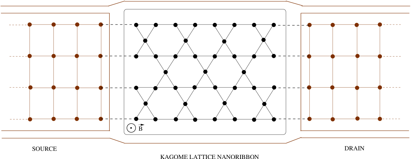
We start with Fig 1, where a finite width kagome lattice ribbon, subject to a perpendicular magnetic field , is attached to two semi-infinite multi-channel leads, commonly known as source and drain. These leads are characterized by the electrochemical potentials and , respectively, under the non-equilibrium condition when an external bias voltage is applied. Both the leads have almost the same cross section as the sample to reduce the effect of the scattering induced by wide-to-narrow geometry at the sample-lead interface. The whole system is described within a single electron picture by a simple tight-binding Hamiltonian with nearest-neighbor hopping approximation.
The Hamiltonian representing the entire system can be written as a sum of three terms,
| (1) |
The first term represents the Hamiltonian for the kagome lattice ribbon which is coupled to two electron reservoirs through conducting leads i.e., source and drain. In Wannier basis the Hamiltonian of the ribbon in non-interacting picture reads as,
| (2) |
where, refers to the site energy of an electron at each site of the kagome ribbon and corresponds to the nearest-neighbor hopping integral between the sites in presence of a perpendicular magnetic field. The effect of magnetic field () is incorporated in the hopping term through the Peierl’s phase factor and for a chosen gauge field it becomes,
| (3) |
where, gives the nearest-neighbor hopping integral in the absence of magnetic filed and () is the elementary flux quantum. The specific choice of the gauge field in this case and the exact
calculation of the Peierl’s phase factor has been discussed in the sub-sequent section. and correspond to the creation and annihilation operators, respectively, of an electron at the site of the nanoribbon.
The second and third terms of Eq. 1 describe the T-B Hamiltonians for the multi-channel semi-infinite leads and sample-to-lead coupling. In Wannier basis they can be written as follows.
and,
| (5) |
Here, and stand for the site energy and nearest-neighbor hopping integral in the leads. and are the creation and annihilation operators, respectively, of an electron at the site of the leads. The hopping integral between the boundary sites of the lead and the sample is parametrized by .
II.2 Calculation of the Peierl’s phase factor
Let us now evaluate incorporating the Peierl’s phase factor.
We choose the gauge for the vector potential associated with the magnetic field (), perpendicular to the lattice plane, in the form,
| (6) |
This specific choice is followed from a literature schr , and the purpose of doing so is solely due to the simplification of the factor along various paths of the ribbon.
With this particular choice of gauge, we determine for the three different types of paths of the ribbon through which an electron can hop in the following ways.
First, we consider the hopping along the axis (see Fig. 2). In this case, our choice of gauge ensures that the component of along
axis is zero i.e., . So, . Therefore, when an electron hops along the axis, either along the , or its parallel direction.
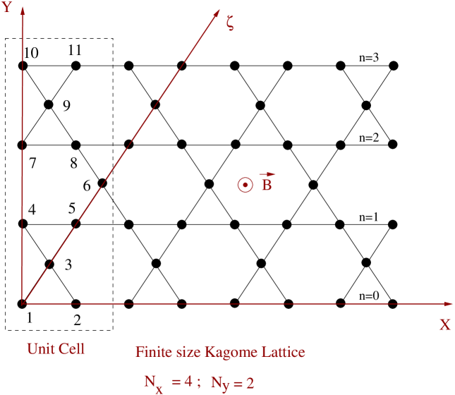
Here, we consider the hopping along the (ve for forward hopping and ve for backward hopping) direction only. In this case . is the lattice spacing. Now, for line, , and therefore, . For the line , , and hence, . If we set , the flux enclosed by the smallest triangle (as shown in Fig. 3), then for the line , . Therefore, in general, we can write the hopping term for -th line as,
| (7) |
where, .
Finally, we consider the case where electrons hop along the direction from site to site and all its parallel directions. In this case,
| (8) |
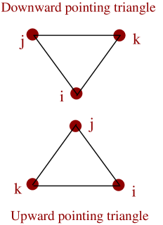
It can be shown by straightforward calculation that for an upward pointing triangle (shown in Fig. 3) the modified hopping strengths are given by,
| (9) |
The value of belongs to the base line of the triangle.
Similarly, for a downward pointing triangle (shown in Fig. 3) the modified hopping integrals can be written as,
| (10) |
Here, , as for a downward pointing triangle the sites and do not belong to the same value of .
II.3 Evaluation of the transmission probability and current by Green’s function technique
To obtain the transmission probability of an electron through such a bridge system, we use Green’s function formalism. Within the regime of coherent transport and in the absence of Coulomb interaction this technique is well applied.
The single particle Green’s function operator representing the entire system for an electron with energy is defined as,
| (11) |
where, .
Following the matrix form of and the problem of finding in the full Hilbert space can be mapped exactly to a Green’s function corresponding to an effective Hamiltonian in the reduced Hilbert space of the ribbon itself and we have,
| (12) |
where,
| (13) |
These and are the contact self-energies introduced to incorporate the effect of coupling of the kagome ribbon to the source and drain. It is evident from Eq. 13 that the form of the self-energies are independent of the conductor itself through which transmission is studied.
Following Lee and Fisher’s expression for the transmission probability of an electron from the source to drain we can write,
| (14) |
’s ( and ) are the coupling matrices representing the coupling between the ribbon and the leads and they are mathematically defined by the relation,
| (15) |
Here, and are the retarded and advanced self-energies associated with the -th lead, respectively.
It is shown in literature by Datta et al. datta1 ; datta2 that the self-energy can be expressed as a linear combination of a real and an imaginary part in the form,
| (16) |
The real part of self-energy describes the shift of the energy levels and the imaginary part corresponds to the broadening of the levels. The finite imaginary part appears due to incorporation of the semi-infinite leads having continuous energy spectrum. Therefore, the coupling matrices can easily be obtained from the self-energy expression and is expressed as,
| (17) |
Considering linear transport regime, at absolute zero temperature the linear conductance is obtained using two-terminal Landauer conductance formula,
| (18) |
With the knowledge of the effective transmission probability we compute the current-voltage (-) characteristics by the standard formalism based on quantum scattering theory.
| (19) |
Here, is the Fermi function corresponding to the source and drain. At absolute zero temperature the above equation boils down to the following expression.
| (20) |
In our present work we assume that the potential drop takes place only at the boundary of the conductor.
II.4 Evaluation of the self-energy
Finally, the problem comes to the point of evaluating self-energy for the finite-width, multi-channel D leads verges ; nikolic . Now, for the semi-infinite leads (source and drain) as the translational invariance is preserved in direction only, the wave function amplitude at any arbitrary site of the leads can be written as, , with energy
| (21) |
In Eq. 21, is continuous, while has discrete values given by,
| (22) |
where, . is the total number of transverse channels in the leads. In our case .
The self-energy matrices have non-zero elements only for the sites on the edge layer of the sample coupled to the leads and it is given by,
| (23) |
where, is the self-energy of the each transverse channel with a specific value of . It is expressed in the following from:
| (24) |
with , when the energy lies within the band i.e., ; and,
| (25) |
when the energy lies outside the band. The sign comes when , while the sign appears when .
III Results and discussion
We begin by referring the values of different parameters used for our calculations. Throughout our presentation, we set and fix all the hopping integrals (, and ) at . We measure the energy scale in unit of and choose the units where . The magnetic flux is measured in unit of the elementary flux quantum .
III.1 Analytical description of energy dispersion relation in presence of magnetic field
To make this present communication a self contained study let us start with the energy band structure of a finite width kagome lattice nano-ribbon. We obtain it analytically.
Here we follow a general approach to evaluate the band structure of a quasi one-dimensional kagome lattice nanoribbon. We establish an effective difference equation similar to the case of an D infinite chain and this can be done by proper choice of a unit cell from the ribbon. The schematic view of a unit cell is shown by the dashed region of Fig. 2. We consider the ribbon to be made up of the unit cells consisting of atomic sites.
Within the tight-binding approximation the effective difference equation for the -th unit cell reads as,
| (26) |
Here, is a column vector with elements representing the wave function at the -th unit cell. is a dimensional matrix and it represents the site-energy matrix of the unit cell. corresponds to the hopping integral between two neighboring unit cells with identical dimension of the site-energy matrix.
Since the system is translationally invariant along the direction, the vector can be written as,
| (27) |
Here,
| (28) |
Substituting the value of in Eq. 26 we have,
| (29) |
The non-trivial solutions of Eq. 29 are obtained from the following condition.
| (30) |
Thus, simplifying Eq. 30, we get the desired energy-dispersion relation ( vs. curve) for the finite width kagome nanoribbon.
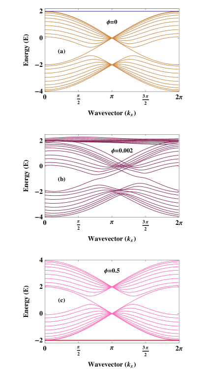
As illustrative example, in Fig. 4 we show the variation of energy levels as a function of wave vector for a finite width
kagome nanoribbon considering for different values of magnetic flux . Most interestingly we see that, when , a highly degenerate and dispersionless flat band appears at (blue line of Fig. 4(a)) along with the dispersive energy levels. But, as long as the magnetic flux is switched on, the degeneracy of the energy levels at the typical energy is broken and the flatness of these levels gets reduced i.e., they start to be dispersive. This feature is clearly observed from Fig. 4(b). Finally, when the flux is set at , the flat band again re-appears in the spectrum and it situates at the bottom of the energy spectrum i.e., at (red line of Fig. 4(c)), which is exactly opposite to that of the case when . This feature provides the central idea for the exhibition of magnetic field induced metal-insulator transition in a kagome lattice ribbon.
III.2 Energy-flux characteristics
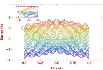
The behavior of single-particle energy levels as a function of flux for a finite size kagome lattice is shown in Fig. 5, where the energy eigenvalues are obtained by diagonalizing the Hamiltonian
matrix. Here we choose and . This - spectrum is sometimes called as Hofstader butterfly spectrum. From the spectrum it is clearly observed that a highly degenerate energy level is present at when is set at zero, and, the application of a very small non-zero flux helps to break the degeneracy which is clearly shown in the inset of Fig. 5. The presence of even a very small magnetic flux affects the phase of the electronic wave functions and thus destroys the quantum interference originated flat band. The flat band again comes back because of the quantum interference effect at the energy when is switched to . The - spectrum is periodic in with periodicity ( in our chosen unit system) and it is mirror symmetric about . For an infinitely large system when , and are two arbitrary integers, magnetic mini-bands appear in the spectrum, and, for i.e., , the number of mini-bands is smallest and the gap becomes widest. But in our case, we do not observe such gaps, as they are smeared out because of the decoherence of the wave functions.
III.3 Length dependence on transmission probability
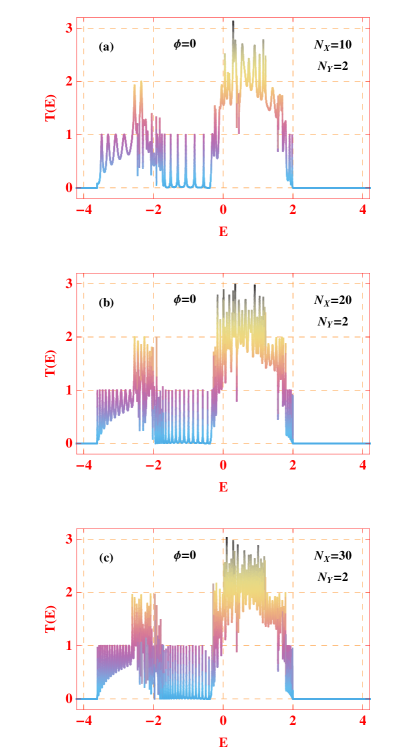
As illustrative example, in Fig. 6, we show the variation of transmission probability as a function of injecting electron energy for a finite size kagome ribbon in the absence of magnetic flux . Here we fix the width () and vary the length of the ribbon. For three different lengths the results are shown in (a), (b) and (c), respectively.
Sharp resonant peaks are observed in the - spectrum associated with the eigenenergies of the ribbon, and therefore, it can be predicted that the transmission spectrum manifests itself the electronic structure of the ribbon. In our numerical calculations, though all the hopping parameters are set to the same value (), but due to the difference
in the geometrical structures of the side attached leads (square lattice) and conductor (kagome lattice), the geometry has double barrier structure which exhibits resonant tunneling conductance. The electrons tunnel from the source to drain via the discrete eigenenergy channels of the ribbon. The height and width of the transmittance peaks are associated with these level widths generated through the coupling mou1 ; mou2 ; san1 of the kagome ribbon to the leads and it is physically related to the time that an electron stays within the ribbon while channeling from the source to drain. As can be seen from the figures that the magnitudes of the peaks are not random, they are quantized to the integer values which corresponds to the number of transverse modes in the leads. With the increase of the length of the ribbon, the number of resonant eigenstates are also increased, and accordingly, the spectrum looks more dense, but the quantized nature and values of remains unchanged as the ribbon width is kept fixed at a certain value.
III.4 Conductance quantization
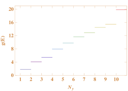
In order to understand the dependence of conductance on the ribbon width , in Fig. 7, we show the variation of two-terminal conductance as a function of in the absence of magnetic flux when is fixed at . The conductance is directly proportional to the number of transverse modes in the leads which is defined by the factor . Following Landauer formula the conductance at k is related to the transmission probability as given in Eq. 18. It gives the total transmission probability of an electron through the ribbon by adding the net contributions of all the channels. Thus we can write,
| (31) |
where, corresponds to the transmission probability between the and -th modes of the two leads. With the increase of , the number of propagating transverse modes () also increases, and therefore, the enhancement in the magnitude of conductance is achieved which is clearly shown in Fig. 7.
III.5 Effect of magnetic flux on transport properties
Now we focus our attention on the effect of magnetic flux on electronic transport through a finite size kagome ribbon. We illustrate it by presenting transmission probabilities and current-voltage characteristics.
III.5.1 Transmission probability and DOS spectra
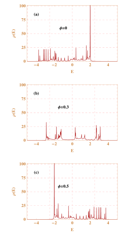
In Fig. (8), we present the variation of transmission probability (right column) along with the nature of density of states (DOS) profile (left column) as a function of energy for a finite size kagome ribbon considering three different values of magnetic flux . In the top of the left column, DOS is shown when is set at . A sharp peak is observed at the right edge of the energy band due to localized states. These states are highly degenerate and are generally pinned at . The existence of these localized states is a characteristic feature of this kind of topology due to quantum interference effect between the electronic wave functions. Correspondingly, in the transmittance spectrum (top of the right column) we obtain transmission peaks at the positions of extended eigenstates but no peak is observed exactly at referring to the localized states.
The presence of an external magnetic field disturbs the phases of the wave functions resulting into annihilation of the localized states and
thus a continuum of extended eigenstates is observed as shown in the middle panel of the left column where is set to an arbitrary value . Accordingly, the transmission peaks are observed and notably finite transmission probability is obtained at , which was zero in the case. This feature bears the crucial importance for showing the property of insulator-to-metal transition.
Finally, when the magnetic flux is set equal to the half flux quantum i.e., , again the quantum interference effect takes place in such a way that the sharp peak associated with the localized states re-appears in the DOS spectrum (bottom of the left column), but now at the left edge () of the energy band. Similarly, for this energy transmission probability vanishes and peaks in the transmittance spectrum are observed where the extended states are situated (bottom of the right column).
III.5.2 Current-voltage characteristics
Here we explore the possibility of magnetic field induced metal-insulator (MI) transition by investigating the current-voltage (-) characteristics through a finite size kagome ribbon. It is shown in Fig. 9, where two different values of are chosen. The current through the nano-structure is obtained via Landauer-Büttiker formalism by integrating over the transmission curve (see Eq. 20). When the equilibrium Fermi level is fixed at , almost zero current is obtained for small bias voltage in the absence of any magnetic field (blue line in Fig. 9(a)) since the localized states, placed at , do not contribute anything in electronic conduction. As the magnetic field is switched on, localization gets destroyed. Therefore, setting at the particular value , sufficiently large current is obtained (red line in Fig. 9(a)) compared to the previous case where no magnetic field is given which yields the metallic behavior. From the careful observation we see that when , the best current magnification is achieved for .
An exactly similar but reverse transition i.e., metal-to-insulator takes place (Fig. 9(b)) when the Fermi level is set at , instead of . When , a large current response (metallic state) is observed due to the presence of extended energy eigenstates around . On the other hand, for , highly degenerate localized states are formed at , and thus, a very low current is achieved in response to the applied bias voltage which leads to the insulating phase.
IV Closing remarks
To summarize, in the present paper we investigate electron transport properties through a finite size kagome lattice nanoribbon attached to two finite width leads by using Green’s function technique within the framework of Landauer-Büttiker formalism. The model quantum system is described by a simple tight-binding Hamiltonian. Following the analytical description of energy dispersion relation of a finite width kagome nanoribbon in presence of magnetic field, we compute numerically the transmittance-energy spectra together with the density of states and current-voltage characteristics. From the energy dispersion curve we see quite interestingly that, at , a highly degenerate and dispersionless flat band appears at . But as long as the magnetic field is switched on the degeneracy at this typical energy is broken and the flatness of these levels gets reduced i.e., they start to be dispersive. Finally, when the flux is set at , the flat band again re-appears and lies at the bottom of the spectrum i.e., at . This phenomenon provides the central idea for the exhibition of magnetic field induced metal-insulator transition in a kagome lattice nanoribbon and it is justified by studying the current-voltage characteristics for two different choices of the equilibrium Fermi energy . Our analysis can be utilized in designing nano-scale switching devices.
The results presented in this communication are worked out for absolute zero temperature. However, they should remain valid even in a certain range of finite temperatures ( K). This is because the broadening of the energy levels of the kagome ribbon due to the ribbon-to-lead coupling is, in general, much larger than that of the thermal broadening datta1 ; datta2 .
References
- (1) K. von Klitzing, G. Dorda, and M. Pepper, Phys. Rev. Lett. 45, 494 (1980).
- (2) J. Sinova, D. Culcer, Q. Niu, N. A. Sinitsyn, T. Jungwirth, and A. H. MacDonald, Phys. Rev. Lett. 92, 126603 (2004).
- (3) C. L. Kane and E. J. Mele, Phys. Rev. Lett. 95, 146802 (2005).
- (4) C. L. Kane and E. J. Mele, Phys. Rev. Lett. 98, 106803 (2007).
- (5) K. Shiraishi, H. Tamura, and H. Takayanagi, Appl. Phys. Lett. 78, 3702 (2001).
- (6) P. Mohan, F. Nakajima, M. Akabori, J. Motohisa, and T. Fukui, Appl. Phys. Lett. 83, 689 (2003).
- (7) P. Mohan, J. Motohisa, and T. Fukui, Appl. Phys. Lett. 84, 2664 (2004).
- (8) K. Kumakura, J. Motohisa, and T. Fukui, J. Cryst. Growth 170, 700 (1997).
- (9) C. Abrecht, J. H. Smet, K. von Klitzing, D. Weiss, V. Umansky, and H. Schweizer, Phys. Rev. Lett. 86, 147 (2001).
- (10) A. Meilke, J. Phys. A 25, 4335 (1992).
- (11) A. Meilke and H. Tasaki, Commun. Math. Phys. 158, 341 (1993).
- (12) T. Kimura, H. Tamura, K. Shiraishi, and H. Takayanagi, Phys. Rev. B 65, 081307(R) (2002).
- (13) H. Ishii, T. Nakayama, and J. I. Inoue, Phys. Rev. B 69, 085325 (2004).
- (14) H. Ishii and T. Nakayama, Phys. Rev. B 73, 235311 (2006).
- (15) S. Datta, Electronic transport in mesoscopic systems, Cambridge University Press, Cambridge (1995).
- (16) S. Datta, Quantum Transport: Atom to Transistor, Cambridge University Press, Cambridge (2005).
- (17) R. Landauer, IBM J. Res. Dev. 1, 223 (1957).
- (18) M. Schreiber, The Aharanov-Bohm ffect in a superconducting lattice, (2005) (unpublished).
- (19) J. A. Vergés, Comput. Phys. Commun. 118, 71 (1999).
- (20) B. K. Nikolić and P. B. Allen, J. Phys.: Condens. Matter 12, 9629 (2000).
- (21) M. Dey, S. K. Maiti, and S. N. Karmakar, Phys. Lett. A 374, 1522 (2010).
- (22) M. Dey, S. K. Maiti, and S. N. Karmakar, Eur. Phys. J. B 80, 105 (2011).
- (23) S. K. Maiti, Phys. Lett. A 373, 4470 (2009).