Epitaxial interfaces between crystallographically mismatched materials
Abstract
We report an unexpected mechanism by which an epitaxial interface can form between materials having strongly mismatched lattice constants. A simple model is proposed in which one material tilts out of the interface plane to create a coincidence-site lattice that balances two competing geometrical criteria—low residual strain and short coincidence-lattice period. We apply this model, along with complementary first-principles total-energy calculations, to the interface formed by molecular-beam epitaxy of cubic Fe on hexagonal GaN and find excellent agreement between theory and experiment.
pacs:
81.15.Aa, 81.15.Hi, 68.55.-a, 68.37.LpA fundamental goal of materials science is to elucidate and exploit the physical principles that govern epitaxial growth Bauer et al. (1990); Palmstrøm (1995). Some of these principles are well-established. For example, if the lattice constants of the film and substrate are close but not identical then a coherently strained film may grow up to a critical thickness, beyond which misfit dislocations relieve the strain Matthews and Blakeslee (1974). Alternatively, a film and substrate having lattice spacings close to an integer ratio may form an epitaxial interface described by a coincidence lattice Sutton and Balluffi (1987); Trampert (2002).
In this Letter we report a new and unexpected mechanism by which epitaxial films can grow on substrates having, in principle, an arbitrary lattice mismatch. We illustrate this mechanism experimentally by growing single-crystal Fe on -plane GaN. The Fe grows in an unusual crystallographic orientation with a very high Miller index, Fe(205). We develop a simple theoretical model which, when complemented with total-energy calculations, correctly predicts this exact orientation as well as the single-domain nature of the film. Finally, we use our model to propose a new strategy for growing nonpolar epitaxial GaN films on high-index Si substrates.
The epitaxial growth of both GaN and Fe was performed in a custom-built molecular-beam epitaxy system equipped with solid-source effusion cells for Ga and Fe. Active nitrogen was provided by a radio-frequency N2 plasma source. Nucleation and growth were monitored in situ by reflection high-energy electron diffraction. A 130-nm thick layer of -plane GaN was first grown on a 4H-SiC substrate under Ga-stable conditions and a temperature of 720∘C. After growth of the GaN layer, excess Ga was desorbed prior to cooling down to 350∘C for the deposition of Fe Brandt et al. (2004). The Fe film grew at this temperature at a rate of 0.13 nm/min to a final thickness of 27 nm. The resulting Fe/GaN/SiC heterostructure was investigated by cross-sectional transmission electron microscopy (TEM) and convergent-beam electron diffraction (CBED) using a JEOL JEM-3010 operating at 300 keV. Electron backscattering diffraction (EBSD) was carried out in a Zeiss Ultra-55 scanning electron microscope equipped with an EDAX-TSL EBSD system.
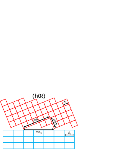
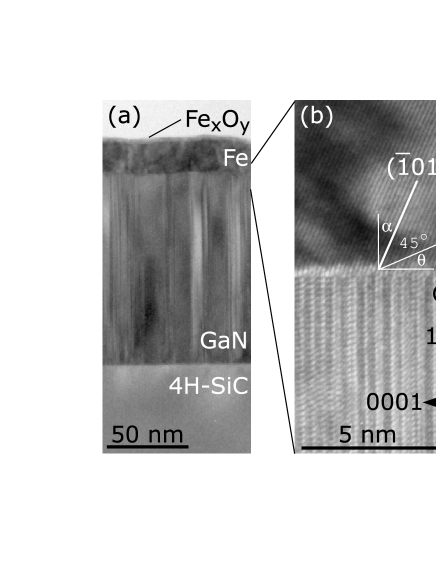
Figure 1(a) shows a cross-sectional transmission electron micrograph of the Fe/GaN/4H-SiC structure. Despite the structural and chemical differences of the constituent materials, the respective layers are well defined and exhibit abrupt interfaces. The GaN layer is seen to contain stacking faults due to the stacking mismatch between 2H-GaN and 4H-SiC. Nevertheless, the high-resolution detail of the Fe/GaN interfacial region shown in Fig. 1(b) reveals an epitaxial relationship between the Fe film and the underlying GaN layer. The (01) lattice planes of the Fe film are clearly resolved and are found to be well ordered, unaffected by the stacking disorder in the GaN layer. Of special interest is the angle, approximately 23∘, formed by the Fe (01) planes and the vertical interface normal. This angle indicates that the Fe interface plane has a high Miller index—an unexpected finding in light of the comparatively high surface energies of high-index metal surfaces. We show now that precisely this orientation is predicted by a simple, physically transparent model (complemented with first-principles total-energy calculations) of epitaxial interfaces between dissimilar materials.
Consider the formation of an interface between a film () and a substrate ( having different lattice constants and . If the lattice mismatch is sufficiently small then the strained film may grow coherently until it reaches its critical thickness Matthews and Blakeslee (1974). For much larger mismatch this scenario becomes unlikely. Epitaxial growth is nevertheless possible by tilting the orientation of the film, as the TEM image in Fig. 1(b) makes clear. Figure 2 illustrates how an arbitrary lattice mismatch can be accommodated by allowing the film to have an orientation between (001) and (101) given by the Miller indices . Our goal below is to predict the most stable film orientation given the lattice constants and .
The unit cell of a film with orientation has length . In order for the film and substrate to be commensurate there must exist a coincidence-site lattice (CSL), defined by a pair of integers , such that . This condition is unrealistically restrictive, however. In real systems the film will tolerate a small compressive or tensile strain which relaxes the CSL condition to .

We propose two geometrical criteria for identifying candidate orientations for interfaces with low energy. (1) The misfit strain should be as small as possible, and (2) the period of the CSL should be as small as possible. The latter criterion is motivated by analogy to low-energy grain boundaries between two identical materials, which often have a CSL with small unit cell volume Sutton and Balluffi (1987). For interfaces between different materials it is not generally possible to minimize the strain and CSL period simultaneously. Nor is it obvious how to construct a single objective function of both which could then be optimized. Instead, we apply both criteria with the aim of selecting a small subset of candidate orientations for subsequent study with a more quantitative method such as density-functional theory (DFT).
To apply these criteria to the growth of Fe on the -plane of GaN we equate with the bcc Fe lattice constant, 2.866 Å Mao et al. (1967), and with the GaN lattice parameter, 5.186 Å Leszczynski et al. (1996). Figure 3 shows the resulting Fe misfit strain needed to satisfy the CSL condition for a large number of hypothetical orientations of the Fe film. In this plot each orientation is represented by its angle relative to the (001) plane. The period of each CSL is encoded by the size of the plot symbol, which is inversely proportional to . Only points with small strains, less than 3%, are displayed here.
The rich structure visible in Fig. 3 makes it clear that the misfit strain can be made arbitrarily small for many different film orientations. Hence the strain alone cannot provide a definitive criterion favoring a particular growth plane. Moreover, the vast majority of these low-strain orientations require a very large CSL period and hence do not constitute physically meaningful commensurability. Only a very few orientations offer both a small strain and small CSL period, namely (207), (205), and (203). The (205) orientation corresponds to the angle . This is equivalent to as defined in Fig. 1(b) and thus is in excellent agreement with the measured angle, 23∘, obtained from TEM.
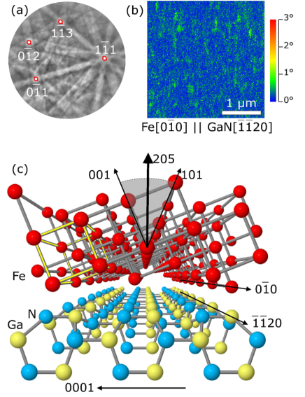
It is important to realize that our purely geometrical criteria do not distinguish between the orientation (205) depicted in Fig. 2 and its symmetry-equivalent counterpart, (20) (), created by rotating the film by 180∘ about the substrate normal. Indeed, the pairs [, ] have the same strain and CSL and hence are equivalent within this model. In the Fe/GaN system, however, the polarity of the GaN wurtzite structure breaks this equivalence. The question that then arises is whether the influence of the polarity is sufficiently strong to select a single orientation, and if so, which one? The TEM image in Fig. 1 shows a single orientation but is limited to a nanometer-scale region of the film. To characterize a much larger area we used EBSD Nolze et al. (2005). Figure 4(a) shows the resulting pseudo-Kikuchi pattern of the Fe film in Fig. 1. The pattern exhibits sharp and well defined Kikuchi bands, reflecting high crystal quality of the Fe film and allowing for a fast and reliable indexing of the patterns recorded while scanning the electron beam over a large area (9 m2). The resulting EBSD map shown in Fig. 4(b) visualizes the in-plane orientation of the Fe film with a spatial and angular resolution of 20 nm and 1∘, respectively. The map reveals the complete absence of any domain structure. Indeed, the film is single crystalline, and has the same orientation as found by TEM throughout the mapped area.
To understand why a single orientational domain is found requires going beyond a model based solely on interface geometry. Now the interface structure—its precise atomic arrangement and chemical bonding—must be addressed. To do this we used DFT to calculate the relative formation energies of finite Fe films grown on the -plane of GaN. We considered the six different orientations predicted by the geometrical model to be favorable: (207), (205), (203), and their rotated counterparts (20), (20), (20). The different films were the same thickness, 6 Å, equivalent to about four monolayers. Figure 4(c) depicts the Fe(205)/GaN interface as an example.
We have previously shown that at 3–4 monolayers the contribution of the Fe/GaN interface formation energy to the full formation energy of the film is already converged Gao et al. (2010). We also find that the Fe free surface energy varies by less than 1 meV/Å2 among the three orientations we consider here Erwin (unpublished). Therefore the relative formation energy of the finite film closely mirrors, with good accuracy, the formation energy of the isolated interface.
For each orientation the Fe film was slightly strained along the [GaN(0001)] direction according to its CSL as discussed above. There is also a lattice mismatch in the [GaN)] direction because the Fe lattice constant and GaN lattice parameter differ by nearly 12%. This mismatch was accommodated by a single CSL, common to all orientations, containing eight unit cells of Fe and seven of GaN. The GaN substrate was represented by a slab of four atomic layers with fixed in-plane equilibrium lattice parameters and a passivating bottom layer. Total energies and forces were calculated within the PBE generalized-gradient approximation Perdew et al. (1996) to DFT using projector-augmented-wave potentials as implemented in vasp Kresse and Hafner (1993); Kresse and Furthmüller (1996). All Fe and GaN atomic positions were fully relaxed except the bottom GaN layer. For each Fe film orientation the formation energy depends strongly on the choice of Fe-GaN interface registry. We systematically varied the registry over a grid in both and to locate the global energy minimum for each orientation. The plane-wave cutoff for all calculations was 400 eV.
The resulting formation energies are listed in Table 1. The most favorable orientation is Fe(205). Of the candidates tested, this orientation has neither the smallest possible strain nor the shortest possible CSL period, indicating that the optimal interface structure is an important third criterion that must supplement the two geometrical criteria. Note also that the small variation in the formation energy of the Fe surface, which is included in the formation energy of the film, is too small to affect the overall energy ordering of the orientations.
| Plane | Misfit strain | CSL period | Formation energy |
|---|---|---|---|
| Fe() | 3 | 0 | |
| Fe() | 3 | 4 | |
| Fe() | 2 | 9 | |
| Fe() | 2 | 16 | |
| Fe() | 4 | 12 | |
| Fe() | 4 | 13 |
To distinguish Fe(205) from Fe(20) experimentally requires determining the absolute polarity of the GaN substrate. We did this by recording CBED patterns with a beam spot size of approximately 15 nm under two-beam conditions. Simulations of CBED patterns were performed using jems sta to index the crystallographic directions observed in the experimental patterns and thus to determine the polarity. The resulting absolute orientation relationship is FeGaN, in agreement with the prediction of our theoretical model complemented with the results of DFT calculations.
Our model suggests a new strategy for growing non-polar GaN films. The basic idea is to turn Fig. 2 upside-down and consider the growth of -plane GaN on a suitable high-index substrate. For a given material this requires identifying candidate orientations corresponding to small strain and small CSL period. One very promising material is Si, which is already in widespread use as a flat substrate for GaN/Si epitaxy despite the resulting high dislocation densities Joblot et al. (2006). Many high-index Si substrates are readily available, and some have already been used for GaN growths Ni et al. (2009); Ravash et al. (2010). Calculations are in progress to identify promising high-index Si orientations for growing nonpolar GaN with low strain Kutana and Erwin (unpublished).
References
- Bauer et al. (1990) E. G. Bauer, B. W. Dodson, D. J. Ehrlich, L. C. Feldman, C. P. Flynn, M. W. Geis, J. P. Harbison, R. J. Matyi, P. S. Peercy, P. M. Petroff, et al., J. Mater. Res. 5, 852 (1990).
- Palmstrøm (1995) C. J. Palmstrøm, Ann. Rev. Mat. Sci. 25, 389 (1995).
- Matthews and Blakeslee (1974) J. W. Matthews and A. E. Blakeslee, J. Crystal Growth 27, 118 (1974).
- Sutton and Balluffi (1987) A. P. Sutton and R. W. Balluffi, Acta Metall. 35, 2177 (1987).
- Trampert (2002) A. Trampert, Physica E 13, 1119 (2002).
- Brandt et al. (2004) O. Brandt, Y. J. Sun, L. Däweritz, and K. H. Ploog, Phys. Rev. B 69, 165326 (2004).
- Mao et al. (1967) H. K. Mao, W. A. Bassett, and T. Takahashi, J. Appl. Phys. 38, 272 (1967).
- Leszczynski et al. (1996) M. Leszczynski, H. Teisseyre, T. Suski, I. Grzegory, M. Bockowski, J. Jun, S. Porowski, K. Pakula, J. M. Baranowski, C. T. Foxon, et al., Appl. Phys. Lett. 69, 73 (1996).
- Nolze et al. (2005) G. Nolze, V. Geist, R. S. Neumann, and M. Buchheim, Cryst. Res. Technol. 40, 791 (2005).
- Gao et al. (2010) C. X. Gao, O. Brandt, S. C. Erwin, J. Lähnemann, U. Jahn, B. Jenichen, and H. P. Schönherr, Phys. Rev. B 82, 125415 (2010).
- Erwin (unpublished) S. C. Erwin (unpublished).
- Perdew et al. (1996) J. P. Perdew, K. Burke, and M. Ernzerhof, Phys. Rev. Lett. 77, 3865 (1996).
- Kresse and Hafner (1993) G. Kresse and J. Hafner, Phys. Rev. B 47, 558 (1993).
- Kresse and Furthmüller (1996) G. Kresse and J. Furthmüller, Phys. Rev. B 54, 11169 (1996).
- (15) P. A. Stadelmann, JEMS electron microscopy software (Java version 3.5110U2010), CIME-EPFL, Switzerland, 1999–2010.
- Joblot et al. (2006) S. Joblot, Y. Cordier, F. Semond, S. Chenot, P. Vénnègues, O. Tottereau, P. Lorenzini, and J. Massies, Superlattices and Microstructures 40, 295 (2006).
- Ni et al. (2009) X. Ni, M. Wu, J. Lee, X. Li, A. A. Baski, Ü. Özgür, and H. Morkoç, Appl. Phys. Lett. 95, 111102 (2009).
- Ravash et al. (2010) R. Ravash, J. Blaesing, A. Dadgar, and A. Krost, Appl. Phys. Lett. 97, 142102 (2010).
- Kutana and Erwin (unpublished) A. Kutana and S. C. Erwin (unpublished).