Influence of cross-section geometry and wire orientation on the phonon shifts in ultra-scaled Si nanowires
Abstract
Engineering of the cross-section shape and size of ultra-scaled Si nanowires (SiNWs) provides an attractive way for tuning their structural properties. The acoustic and optical phonon shifts of the free-standing circular, hexagonal, square and triangular SiNWs are calculated using a Modified Valence Force Field (MVFF) model. The acoustic phonon blue shift (acoustic hardening) and the optical phonon red shift (optical softening) show a strong dependence on the cross-section shape and size of the SiNWs. The triangular SiNWs have the least structural symmetry as revealed by the splitting of the degenerate flexural phonon modes and The show the minimum acoustic hardening and the maximum optical hardening. The acoustic hardening, in all SiNWs, is attributed to the decreasing difference in the vibrational energy distribution between the inner and the surface atoms with decreasing cross-section size. The optical softening is attributed to the reduced phonon group velocity and the localization of the vibrational energy density on the inner atoms. While the acoustic phonon shift shows a strong wire orientation dependence, the optical phonon softening is independent of wire orientation.
I Introduction
Silicon nanowires (SiNWs) have the potential to become the next generation solution for improved (i) Complementary-Metal-Oxide-Semiconductor (CMOS) transistors with higher channel drive currents Sinwfet , (ii) thermoelectric (TE) devices Hochbaum2008 , (iii) rechargeable batteries sinw_battery , (iv) compact non-volatile memories sinw_nvm , (v) solar cells, sinw_solar_cells and (vi) explosive and bio-sensors sinw_explosive_sensor ; sinw_biosensor . Extensive application of SiNWs to various technologies requires to understand the structural SINW_110_phonon , electricalanantram_ph , thermalMingo_kappa and optical sinw_solar_cells properties which arise from the strong geometrical confinement, atomic positions, and increased surface-to-volume ratio (SVR). Especially the phonon spectra of SiNWs can provide a lot of vital information about their structural properties which can be optimized for maximum technological benefits in SiNWs.
Engineering the Si nanowire structural properties based on their cross-section size has been studied extensively exp_opt_phonon_sinano ; exp_ac_phonon ; mahan_111 ; hepplestone_sinw_2 . However, the impact of cross-section shape has not been completely addressed yet. Experimentally, the impact of semiconductor (GaAs, GaP, ZnS, etc) nanowire shape on their structural properties has been observed shape_dep_raman ; shape_dep_1 ; shape_eff_phd . Motivated by these experiments, we theoretically explore the effect of the cross-section geometry of ultra-scaled SiNWs on their structural properties like phonon shifts. We furthermore provide analytical expressions for the variation of these physical quantities with size and shape thus, enabling (i) physical insights, and (ii) a compact modeling representation of the structural properties.
The determination of size and stability of SiNWs is crucial for their usage in different applications Sinwfet ; sinwfet2 ; Hochbaum2008 ; Boukai2008 ; sinw_battery ; sinw_nvm ; sinw_solar_cells ; sinw_explosive_sensor ; sinw_biosensor . Raman spectroscopy provides a valuable, non-destructive method to analyze the physical properties of nanostructures (NS) like cross-section size exp_ac_phonon ; exp_opt_phonon_sinano , degree of crystallinity adv_RS_method , dimensionality of confinement exp_opt_phonon_sinano ; size_dep_red_shift , etc. Raman spectroscopy utilizes the amount of phonon spectrum shift and line width broadening to obtain useful structural information arora_opt_phonon .
The first satisfactory theoretical model for explaining Raman shifts and line width broadening was proposed by Richter et al Richter and improved by Campbell and Fauchet Campbell . These phenomenological continuum models are based on the choice of the phonon weighting function as well as the boundary conditions of the phonon vibrations Richter ; Campbell which are chosen rather arbitrarily and hence do not provide correct phonon shift in nanostructures Zi_PRB . Arora et al. experimentally arora_opt_phonon reported that phonon shifts are very different from bulk in nanostructures with size less than 20nm. Tanaka et al Tanaka also pointed out the failure of continuum models to predict the Raman shift in nanostructures with size 7.5nm due to the arbitrary parameter sets used in continuum models. While continuum models can match the experimental Raman spectroscopy data using fitting parameters, they lack the predictive capability for estimating the phonon shifts and line widths in nanostructures with different shapes and compositions Zi_PRB ; Tanaka ; raman_size_dep .
The evident inability of the continuum models to properly explain and predict the structural properties in nanostructures Zi_PRB ; Tanaka ; raman_size_dep demands for methods which can automatically take into account the effects of structural miniaturization like geometrical confinement, orientation effects, cross-sectional shape and surface-to-volume ratio effects.
Many efforts to explain the phonon shifts in nanostructures have been reported. They are based on models like the VFF approach VFF_kanelis ; mahan_111 , partial density approach Zi_PRB , Bond Charge Model (BCM) hepplestone_sinw_1 ; hepplestone_sinw_2 , bond order model raman_size_dep , etc. In all these approaches the importance of taking into account the atomic positions and the atomic surrounding to understand the Raman shift has been stressed which most of the continuum models lack Richter ; Campbell .
We utilize a Modified Valence Force Field (MVFF) phonon model VFF_mod_herman ; jce_own_paper ; iwce_own_paper to study the physical properties of SiNWs. This MVFF model (i) is relatively straight forward to understand and implement, (ii) explains the experimental phonon and elastic properties of zinc-blende materials very well VFF_mod_herman ; VFF_mod_zunger ; jce_own_paper ; VFF_kanelis , and (iii) is computationally very efficient which allows for expanding the simulation domain easily to few million atoms anharmonic . However, frozen phonon models like the MVFF one do not integrate thermodynamics which forbids the correct calculation of many physical properties such as low temperature volume thermal expansion. Yet these models give a good insight into the physical processes governed by the lattice under ambient conditions.
The paper is organized as follows. Section II provides a brief introduction about the MVFF model for the calculation of phonons in SiNWs and about the method to extract the phonon shifts in these nanowires (Sec. II.2). The results section (Sec. III) discusses the effect of cross-section shape and size on the phonon spectra (Sec. III.1) and presents experimental benchmarking of the phonon shifts using the MVFF model (Sec. III.2). Furthermore, the trends of the acoustic phonon shift (Sec. III.3) and the optical phonon shift (Sec. III.4) are discussed along with wire orientation dependence (Sec.III.5). Conclusions are provided in Section IV.
II Theory and Approach
II.1 Phonon model
In the MVFF model, the frequencies of the phonon modes are calculated from the forces acting on atoms induced by finite displacements of the atoms from their equilibrium positions in a crystal phon_rev_paper . To calculate the restoring force(F), first the total potential energy of the solid (U) is estimated. For the MVFF model, U is approximated as jce_own_paper ,
| (1) | |||||
where , and represent the total number of atoms in one unit cell, the number of nearest neighbors for atom ‘i’, and the coplanar atom groups for atom ‘i’, respectively. The first two terms and represent the elastic energy coming from bond stretching and bending between the atoms connected to each other as given in the original Keating VFF model Keating_VFF . The terms , and represent the cross bond stretching VFF_mod_herman , cross bond bending-stretching VFF_mod_zunger , and coplanar bond bending VFF_mod_herman interactions, respectively. The detailed procedure for obtaining the phonon spectra in Si bulk and NWs are provided in Ref.jce_own_paper ; iwce_own_paper . In the following sections the method to extract the acoustic and optical phonon shifts and the types of SiNWs used in this study are discussed.
II.2 Phonon shift in Si nanowires
The vibrational spectra of the nanostructures are strongly influenced by (i) the finite size of the nanostructures, (ii) the mismatch with the matrix material ( the surrounding atoms) or (iii) defects arora_opt_phonon ; exp_ac_phonon ; adv_RS_method . The optical and the acoustic phonon energies are shifted compared to the bulk values (around ) in these geometrically confined structures. Raman spectroscopy reveals the decrease of the optical frequency with down-scaling of the nanostructures (called the optical softening or optical red shift) raman_size_dep ; jusserand and the increase of the acoustic frequency (called the acoustic hardening or acoustic blue shift) exp_ac_phonon ; raman_size_dep . These phonon shifts are estimated using the following relation raman_size_dep ; hepplestone_sinw_1 ; hepplestone_sinw_2 ,
| (2) |
where is the bulk acoustic (optical) phonon frequency at the point. The phonon shifts show the following functional dependence on the nanostructure cross-section size (W) raman_size_dep ; exp_opt_phonon_sinano ; hepplestone_sinw_1 ,
| (3) |
where is the lattice constant of the material. For A0 the phonon shift is positive (or blue shift) and for A0 the shift is negative (or red shift) raman_size_dep . The exponent value ‘d’ indicates the dimensionality of the geometrical confinement. For 1D nanowires/nanorods a variety of ‘d’ values have been reported in the literature like 0.67 hepplestone_sinw_1 , 0.95 SINW_110_phonon , 1.44exp_opt_phonon_sinano , etc.
Using a series of Raman spectroscopy measurement for a sample of nanostructures the size and the dimensionality of the nanostructures can be predicted arora_opt_phonon ; raman_size_dep ; shape_dep_raman . The phonon shifts observed in Raman spectroscopy can be predicted using the phonon spectrum. Atomistic phonon modeling correctly takes surface boundary conditions into account depending on the cross-section shape of the wire which reflects in the overall phonon spectrum. The surface and inner atomic movements vary with different cross-section shapes and therefore affects the phonon shifts. Equation 3 captures the nanostructure size effect in the exponent value ‘d’ and the shape effect in the pre-factor ‘A’. Thus, a combination of A and d can be useful for the determination of size and shape of the SiNWs.
II.3 Si Nanowire details
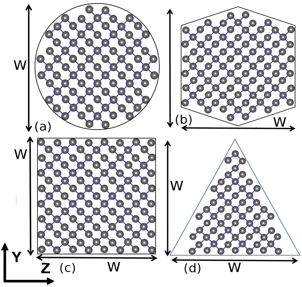
Four cross-section shapes for 100 oriented SiNWs have been considered in this study, (a) circular, (b) hexagonal, (c) square and (d) triangular cross-section shapes (Fig. 1). SiNWs with [110] and [111] channel orientation studied here are of square cross-section only. The feature size is determined by the width parameter W. The value of W is varied from 2 to 6 nm. The surface atoms are allowed to vibrate freely without any passivating species. The wires are still assumed to have a tetrahedral geometry. It has been shown that wires with diameter below 2nm tend to lose the tetrahedral structure sinw_stability ; Amrit due to surface pressure and internal strain.
III Results and Discussion
In this section the effect of cross-section on the phonon dispersion and phonon shifts of 100 SiNWs are discussed.There is a lack of proper channel orientation information in the literature. However Adu et al. shape_dep_shift_exp reported 100 channel orientation due to which we chose [100] SiNWs for shape study. Furthermore, we also investigate the impact of channel orientation on the phonon shifts in square SiNWs.
III.1 Phonon dispersion
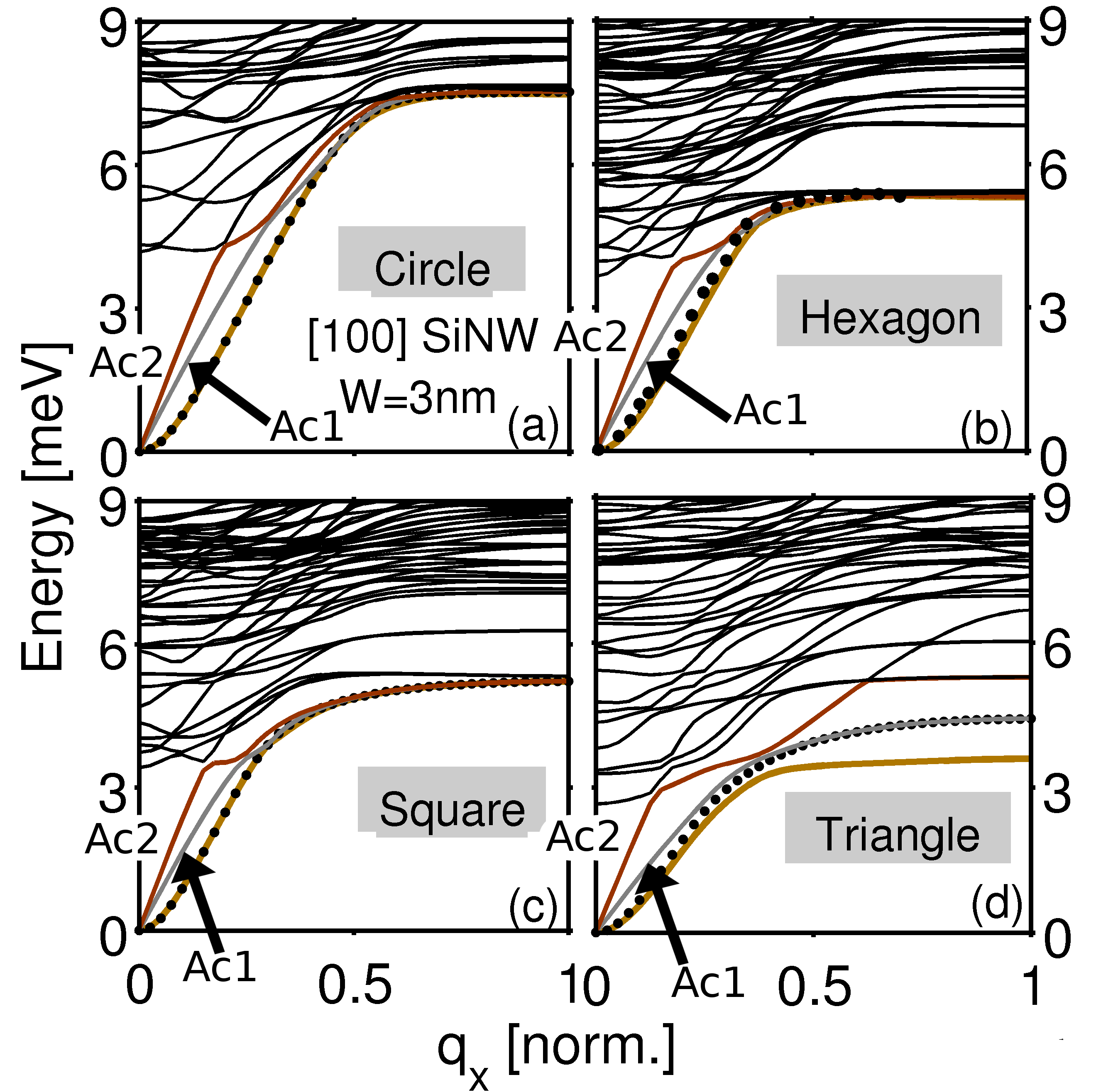
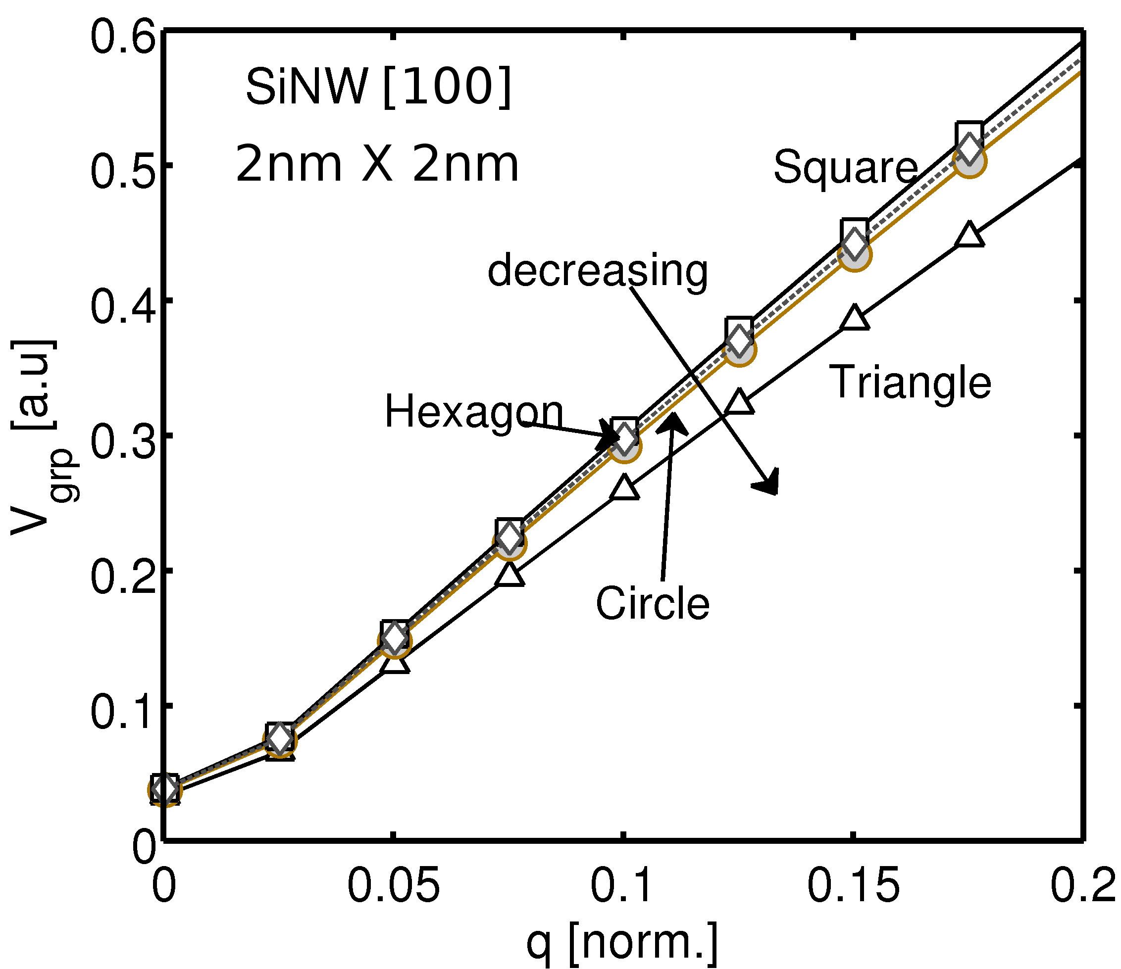
The phonon dispersion of SiNWs for all the cross-section shapes with 100 channel are shown in Fig. 2. While the full phonon dispersion extends up to 65meV, phonon modes till 9 meV energy range are shown for clarity. All the wires exhibit two flexural branchesiwce_own_paper (). These modes are double degenerate in all the shapes except the triangular wire. In the triangular wires these modes split due to the reduced structural symmetry (Fig. 2 d). The next two phonon branches in all the structures show . These branches determine the sound velocity in these structures iwce_own_paper (Table 1). The triangular wire has the lowest longitudinal and transverse sound velocity () whereas other shapes have very similar sound velocities. The splitting of the degenerate flexural modes and the reduced sound velocity show that triangular wires have the least structural symmetry.
III.2 Experimental Benchmark
Before using the MVFF model to calculate phonon frequency shifts it is important to compare the theoretical MVFF results with experimental data. Both the experimental acoustic and optical phonon shifts in Si nanocrystals are compared.
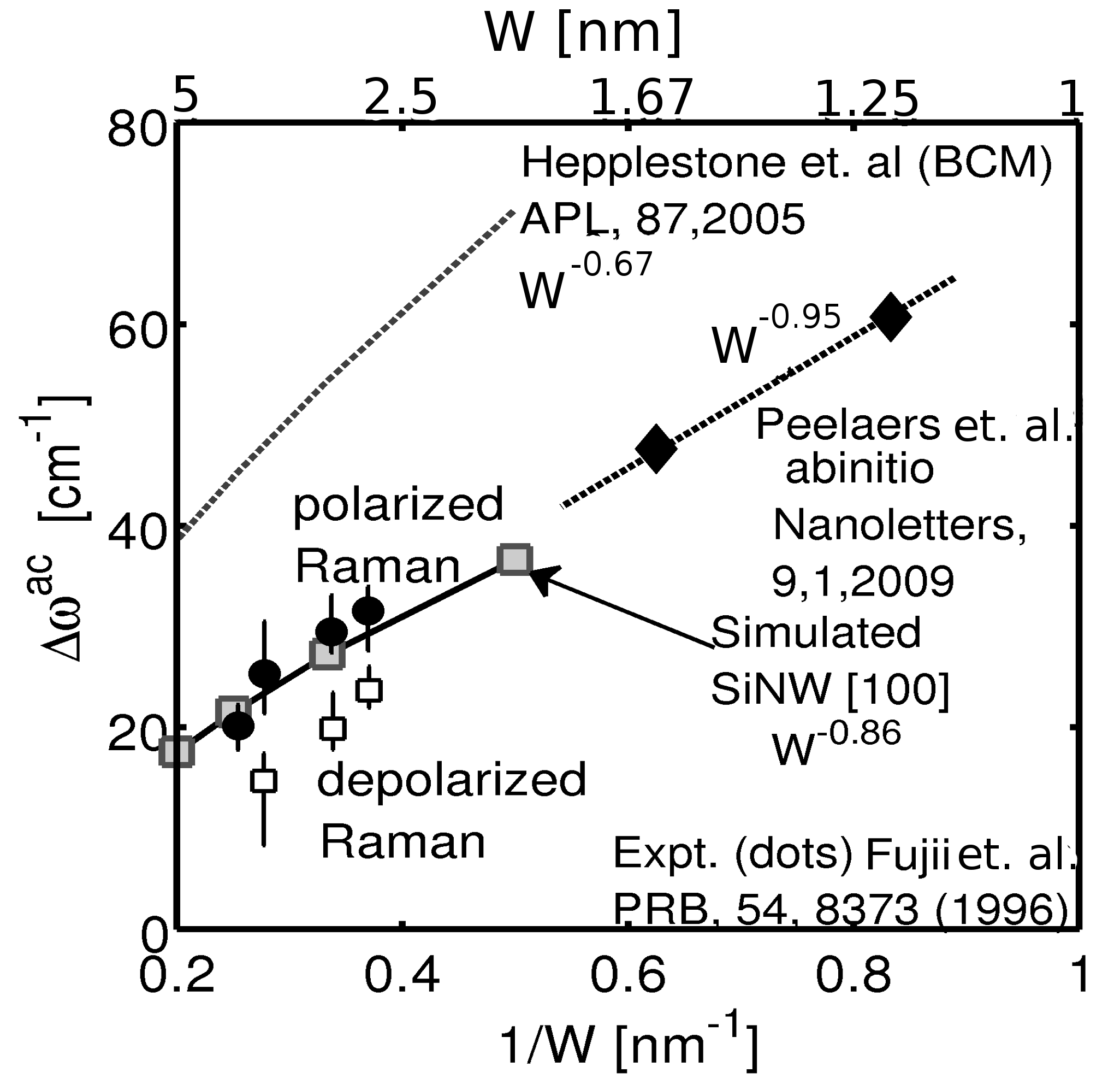
Acoustic shift: The experimental values of acoustic phonon confinement (shown as dots with error bars in Fig. 3) using Raman spectroscopy for Si nanocrystals embedded in a matrix have been reported by Fujii et. al exp_ac_phonon . The calculated acoustic phonon shifts in similar size free-standing circular 100 SiNWs using the MVFF phonon model compare quite well to the experimental data as shown in Fig. 3, providing frequency shifts between 20 and 30 . The MVFF calculated values show a power law of close to the results for 110 SiNWs (diamond dots in Fig. 3) from Ref. SINW_110_phonon (). The difference in the power laws may arise from the wire surface passivation, structural relaxation and channel orientation. The theoretical predictions using the BCM model hepplestone_sinw_2 gives a cross-section dependence of which overestimates the experimentally observed acoustic phonon shift (Fig. 3).
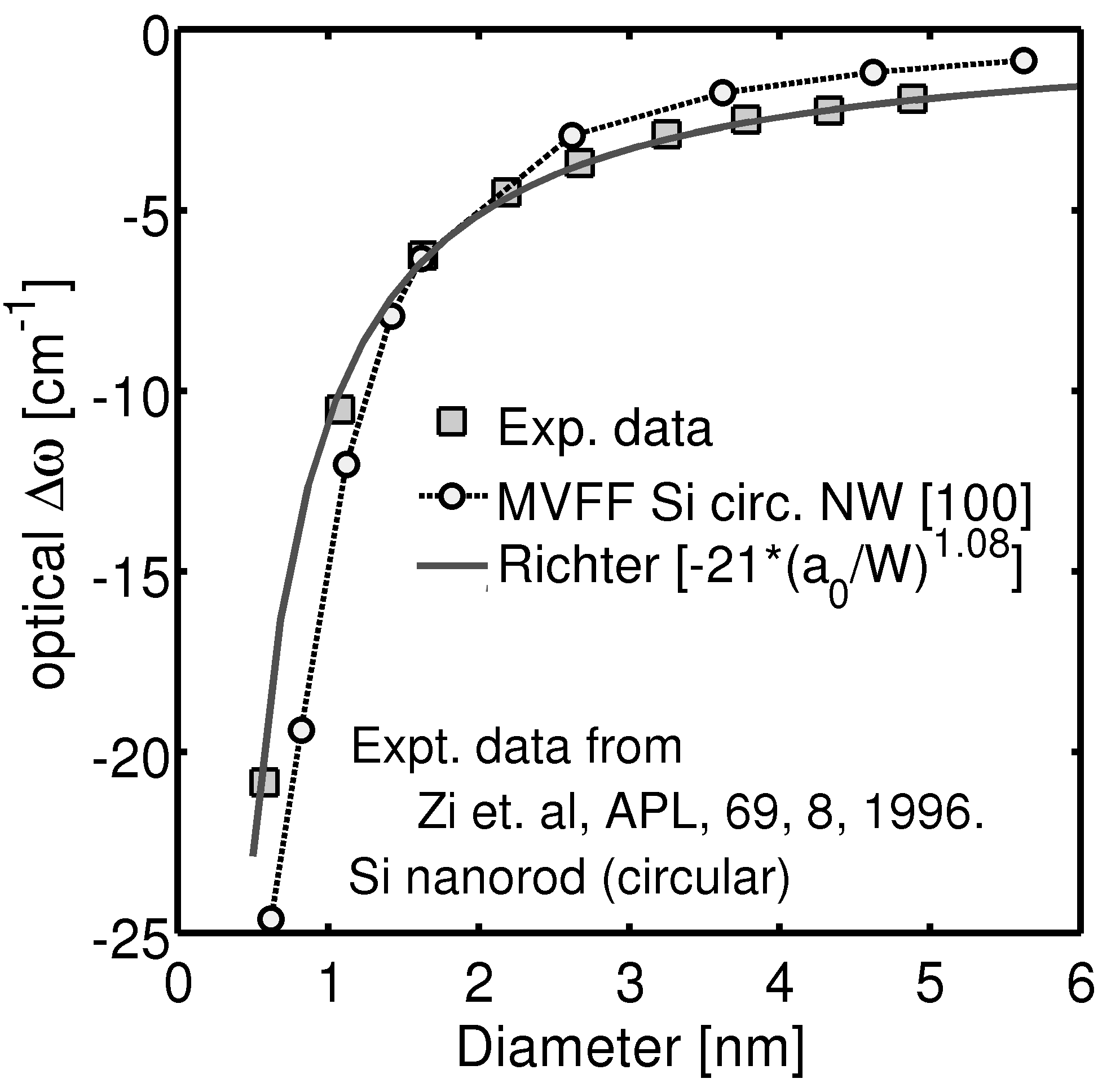
Optical shift: The optical phonon shift is experimentally measured using Raman spectroscopy exp_opt_phonon_sinano ; shape_dep_raman . Figure 4 shows the experimental optical phonon shift result for Si nanorods (symbols) embedded in a matrix. With decreasing cross-section size the optical red-shift increases raman_size_dep . The theoretical optical phonon shift is calculated for free-standing 100 circular SiNWs using the MVFF model. The theoretical values of the optical shift agree well with the experimental data (Fig. 4). The mismatch in phonon shifts at extremely small dimensions () may be due to, (i) the structural relaxation in small cross-section wires sinw_stability ; Amrit which is not taken into account in this study and (ii) the presence of around SiNWs which might affect the results for smaller wires though the overlap of the optical phonon spectrum of these two materials is small arora_opt_phonon . Hence, the MVFF model correctly captures the optical phonon shifts in SiNWs for W2nm, however, for the MVFF phonon values without structural relaxation are not very accurate. Though the optical shift is very well captured by the Richter model Richter , the fitting parameters are chosen arbitrarily which removes the predictive capability from the model.
In the next few sections we will discuss the structural properties of ultra-scaled SiNWs with different cross-section shapes and sizes.
III.3 Acoustic Phonon shift in SiNWs
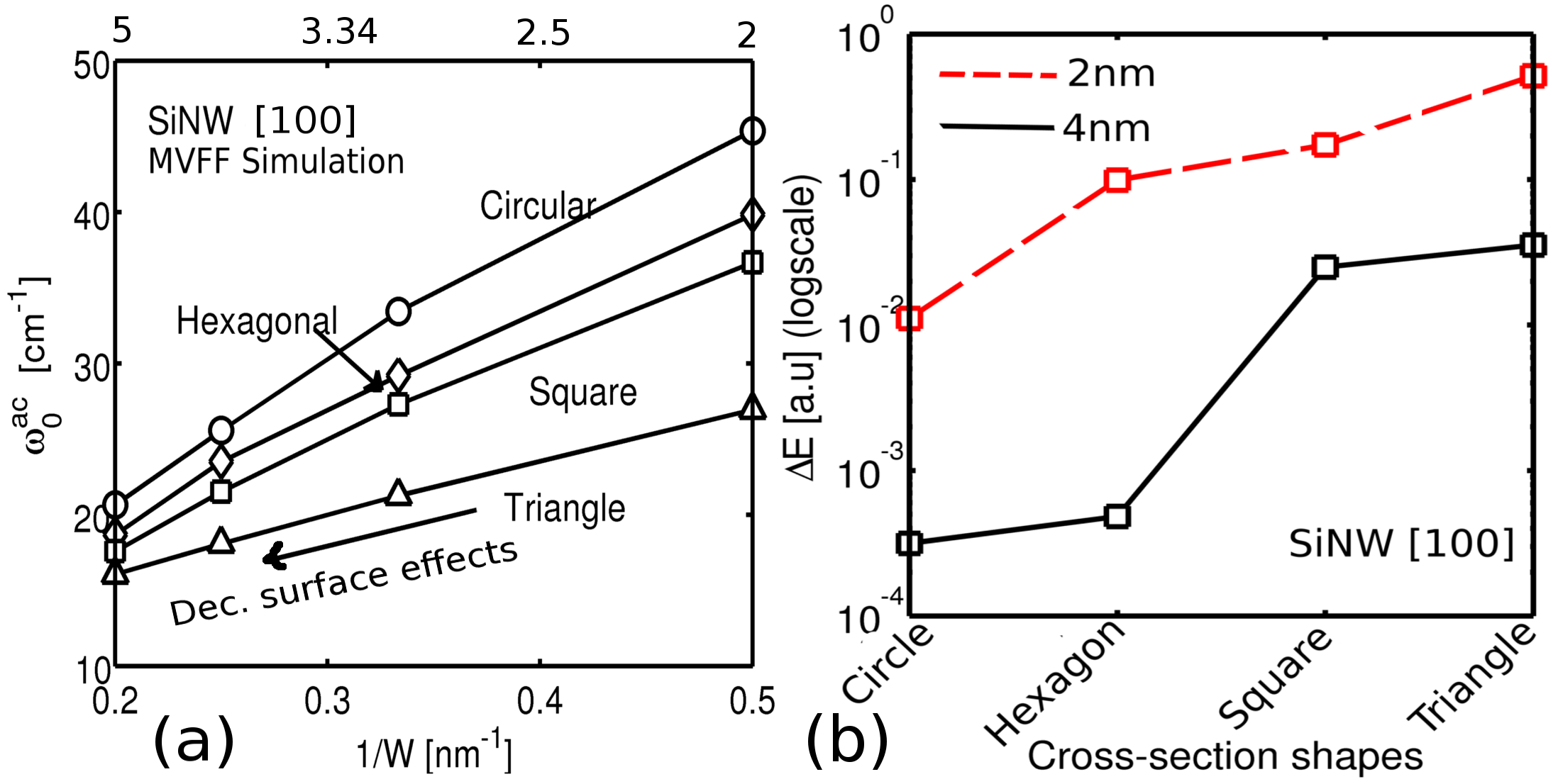
Influence of cross-section shape and size: The acoustic phonon shifts are calculated using the MVFF model for different cross-section shaped SiNWs. All the wire geometries show a blue shift of the acoustic mode (this mode closely resembles the ‘radial breathing mode’ observed in perfectly circular wires SINW_111 ) as the wire cross-section size is reduced (Fig. 5 a). There is a clear cross-section shape dependence of the blue shifts where the blue shift follows the order . The power exponent () varies between 0.6 and 0.856 (Table 2). The order of the pre-factor () in Eq. (2) value (Table 2) also shows the order of the acoustic blue shift for 100 SiNWs.
With the increase in wire cross-section size two important things happen, (i) the geometric confinement on the phonons reduces, and (ii) the vibrational energy deviation between the surface and the inner atoms decreases (Fig. 5. First point explains the reduction in the blue shift with increase in cross-section size for all the SiNWs while the second point explains the order of blue-shift with shape.
As the SiNW cross-section is reduced lots of low velocity phonon sub-bands start to appear above the acoustic branches (Fig. 2) which are normally absent in bulk. These relatively flat bands cause phonon confinement. These zone center low energy phonon sub-bands cause acoustic blue shift. The surface atom vibrations become comparable to the inner core atom vibrations with size reduction. The blue shift is more pronounced when surface modes are less dominant. If the surface atoms vibrations are more than inner atoms then blue shift is suppressed raman_size_dep .
The acoustic blue shift order can be explained by the difference between the vibrational energy density li_hollow_sinw of the surface atoms and the inner atoms (E). Surface atoms are the ones with dangling bonds. The spatial vibrational energy density can be calculated as li_hollow_sinw ,
| (4) |
where NA is the total number of atoms in the unit cell, ‘i’ is the phonon sub-band, ‘q’ is the phonon wave-vector, ‘j’ is the polarization, is Bose-Einstein distribution for phonon population, is the phonon eigen frequency for sub-band ‘i’ and wave-vector ‘q’ and is the phonon eigen vibration mode.
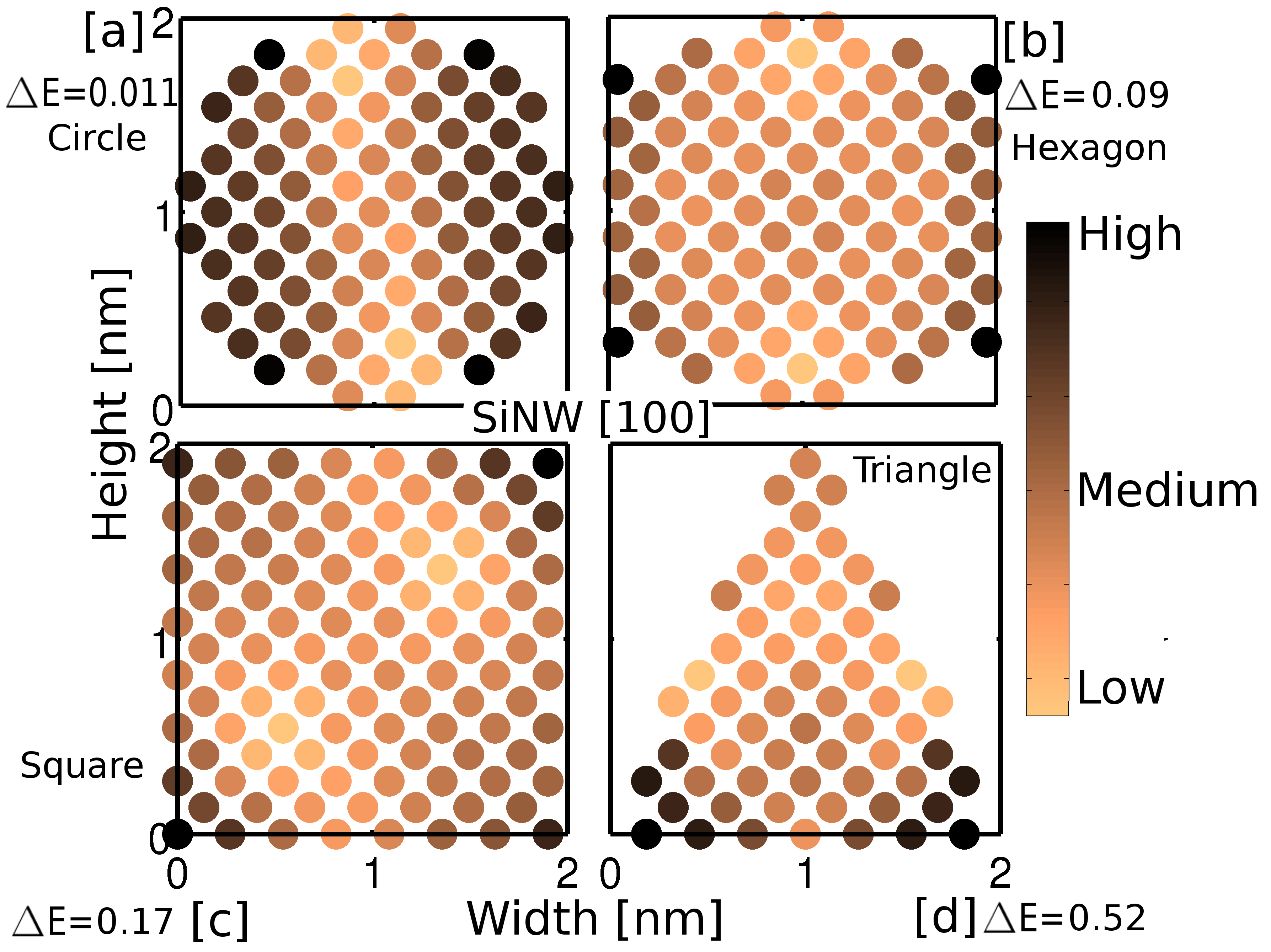
Figure 5 b shows that the triangular wire exhibits the maximum difference between the surface and inner atom vibrational energy density for W = 2nm and 4nm, followed by the square, the hexagonal, and the circular wire. Figure 6 shows the spatial distribution of the energy density for the acoustic phonon branch for 2nm cross-section SiNWs. The surface atoms vibrate more intensively compared to the inner atoms. In circular and hexagonal nanowires all atoms vibrate with a similar intensity as indicated by the small E value. However, in square and triangular wires the surface atoms vibrate more compared to the inner atoms leading to a larger E value.
The low frequency acoustic phonon modes are very similar to the breathing mode found in larger circular wires mahan_111 . These eigen frequencies follow a law (Fig. 5), with d = 1 for a perfectly concentric circular wire mahan_111 . The value of ‘d’ deviates from 1 as the cross-section shape deviates from the ideal circular geometry.
III.4 Optical Phonon shift in SiNWs
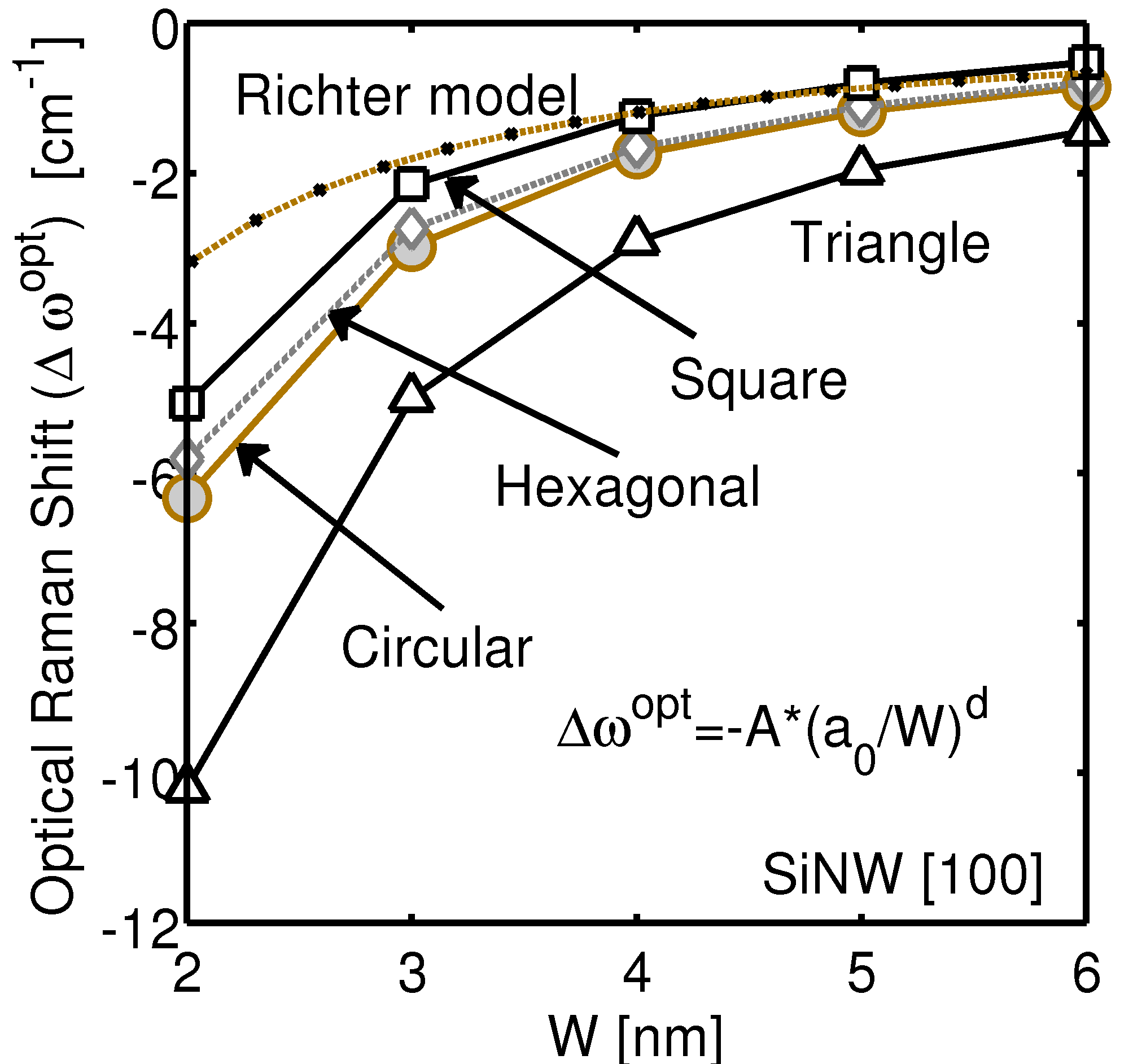
Influence of cross-section shape and size: For optical phonon shift the MVFF model predicts a width exponent factor between 1.8 and 2 (Table 3) for all the cross-section shapes. The 100 triangular SiNWs show the maximum optical red shift () whereas the square SiNWs show the minimum optical red shift (, close to the prediction in Ref.hepplestone_sinw_2 ) (Fig. 7). Furthermore, with decreasing cross-section size (W) all the wires show an increasing optical red-shift (Fig. 7).
Many explanations have been reported in the literature for the optical red-shift in nanostructures like, the increasing surface-to-volume ratio (SVR) raman_size_dep ; size_dep_red_shift , compressive strain adv_RS_method , surface defects surface_disorder and optical phonon confinement size_dep_red_shift ; Richter ; Campbell ; continuum_model . In the present study of free-standing SiNWs the observed shape and size dependence can be explained using the vibrational energy density li_hollow_sinw of the optical mode as well as the optical phonon group velocity () iwce_own_paper .
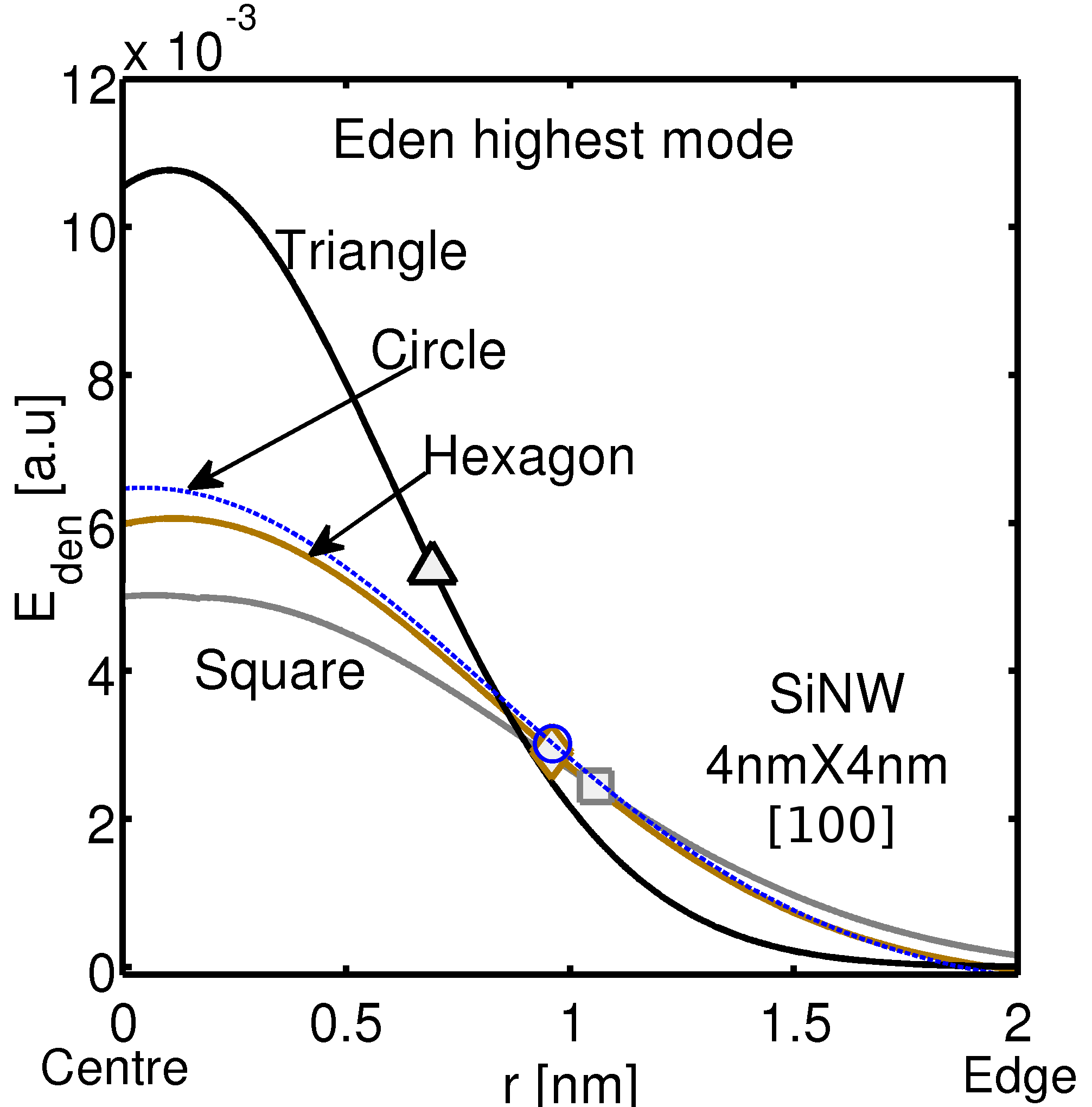
Figure 8 shows the spatial distribution of the vibrational energy density for the optical mode in SiNWs with W = 4nm. The structure with the maximum spatial spread of the energy density has the most active optical modes raman_size_dep since surface atom vibrations contribute to the optical modes. The symbols in Fig. 8 show the FWHM extent of the energy density. The square wire has the maximum energy spread while the triangular wire has the minimum energy spread which explains the highest red-shift in the triangular wires (least active optical modes). As the SiNW dimensions decrease, the energy spread also decreases which increases the red shift for all the shapes.
Another reason for the red-shift can be attributed to the phonon group velocity. Figure 9 shows that the triangular wire has the smallest group velocity whereas the square wire has the highest group velocity. A smaller group velocity implies higher phonon confinement continuum_model . Thus, the phonon group velocity gives the following order of optical phonon confinement; triangular circular hexagonal square. Higher phonon confinement results in more red-shift. This again explains the observed shape dependence of optical red-shift in 100 SiNWs.
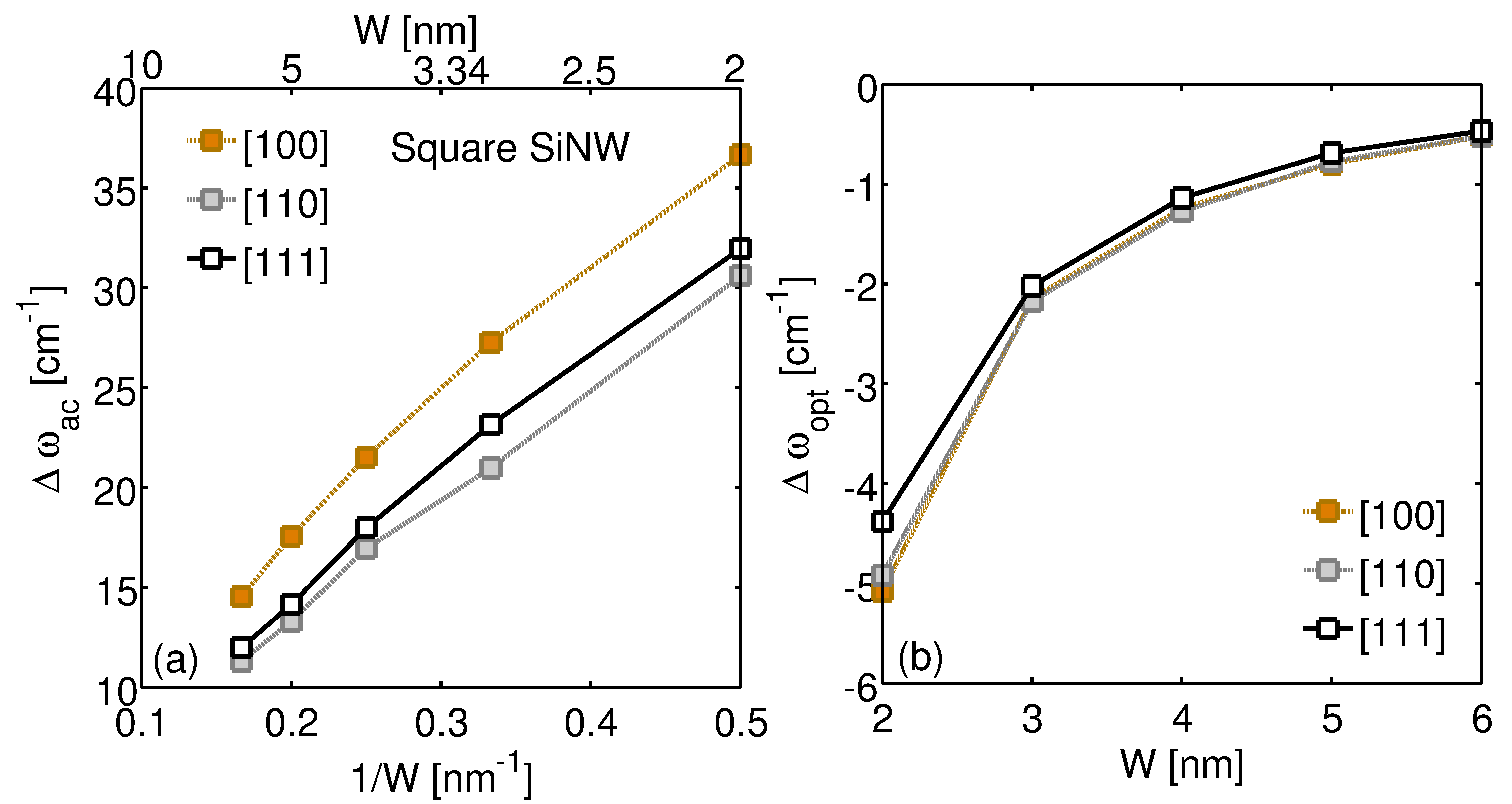
III.5 Orientation effect on phonon shifts
Along with the shape and size of the SiNWs, the wire axis direction can also produce different phonon shifts. This indicates that the confined phonon dispersion is anisotropic. For brevity we present the orientation effects for square SiNWs only, however, these trends are also valid for other shapes. The acoustic phonon shift and the optical phonon shifts are shown in Fig. 10 a and b, respectively. The acoustic phonon blue shift exhibits a strong anisotropy (Fig. 10 a), however, the optical red shift has a very weak orientation dependence (10 b). This observed behavior of phonon shift can be explained by the phonon dispersion anisotropy in Si. In Si the maximum phonon frequency of the acoustic branch along [100], [110] and [111] directions are highly anisotropic VFF_mod_herman ; jauho_method , whereas the maximum frequency of the optical branches are isotropic (519.3 ). The acoustic blue shift show the following behavior . The cross-section size dependence for both kind of phonon shifts are provided in Table. 4. The acoustic phonon shift exponent of [110] wires is 0.89 which compares reasonably to the exponent of 0.95 observed for [110] SiNWs in Ref. SINW_110_phonon (see Fig. 3).
III.6 Discussion
The phonon spectrum shift in SiNWs with shape, size and orientation is useful in understanding the experimental Raman shifts. The analytical expressions for the shifts can provide a good idea about the structure of the SiNWs which can be helpful in determining properties such as phonon-photon interactions. The evolution of the phonon shifts with increasing size also reflects the size (Wlim) at which the shape effects may be no more distinguishable using Raman spectroscopy. From the expresssions of the phonon shifts (Eq. 2) the Wlim value for acoustic blue shift comes out to be roughly 7nm and for optical shifts this value is 10nm. The analytical expressions are well suited for calculating the vibrational energy shifts depending on different physical aspects of the SiNWs.
IV Conclusion
We have used a MVFF model to calculate the acoustic and optical phonon shifts in SiNWs. The theory agrees quite well with the experimental Raman shift data. At the nanometer scale the acoustic phonon shift is quite sensitive to the (i) wire cross-section size and shape, and (ii) wire channel orientation whereas the optical phonon shift is mainly controlled by the wire cross-section shape and size. The different width exponents and the pre-factors from the acoustic and optical phonon shifts can become a useful tool in predicting the size and shape of the SiNWs. Triangular wires show the highest optical phonon confinement and the least structural symmetry. Analytical expressions for the shape and size dependence of the phonon shifts are useful for compact modeling of physical properties of ultra-scaled SiNWs.
Acknowledgment
The authors acknowledge financial support from MSD Focus Center, under the Focus Center Research Program (FCRP), a Semiconductor Research Corporation (SRC) entity, Nanoelectronics Research Initiative (NRI) through the Midwest Institute for Nanoelectronics Discovery (MIND), NSF (Grant No. OCI-0749140) and Purdue University. Computational support from nanoHUB.org, an NCN operated and NSF (Grant No. EEC-0228390) funded project is also gratefully acknowledged.
References
- (1) N. Singh, A. Agarwal, L. K. Bera, T. Y. Liow, R. Yang, S. C. Rustagi, C. H. Tung, R. Kumar, G. Q. Lo, N. Balasubramanian, and D. L. Kwong, IEEE Electron Dev. Lett. 27, 383 (2006).
- (2) A. I. Hochbaum, R. Chen, R. D. Delgado, W. Liang, E. C. Garnett, M. Najarian, A. Majumdar, and P. Yang, Nature 451, 163 (2008).
- (3) C. K. Chan, H. Peng, G. Liu, K. McIlwrath, X. F. Zhang, R. A. Huggins, and Y. Cui, Nature Nanotechnology 3, 31 (2007).
- (4) Q. Li, X. Zhu, H. D. Xiong, S.-M. Koo, D. E. Ioannou, J. J. Kopanski, J. S. Suehle, and C. A. Richter, Nanotechnology 18, 235204 (2007).
- (5) E. Garnett and P. Yang, Nano Letters 10, 1082 (2010).
- (6) Y. Engel, R. Elnathan, A. Pevzner, G. Davidi, E. Flaxer, and F. Patolsky, Angewandte Chemie International Edition 49, 6830 (2010).
- (7) X. P. A. Gao, G. Zheng, and C. M. Lieber, Nano Letters 10, 547 (2010).
- (8) H. Peelaers, B. Partoens, and F. M. Peeters, Nano Letters 9, 107 (2009).
- (9) A. Buin, A. Verma, and M. Anantram, Journal of Applied Physics 104, 053716 (2008).
- (10) N. Mingo and L. Yang, Phys. Rev. B 68, 245406 (Dec 2003).
- (11) J. Zi, H. Buscher, C. Falter, W. Ludwig, K. Zhang, and X. Xie, Applied Physics Letters 69, 200 (1996).
- (12) M. Fujii, Y. Kanzawa, S. Hayashi, and K. Yamamoto, Physical Review B 54, 8373 (1996).
- (13) T. Thonhauser and G. D. Mahan, Phys. Rev. B 71, 081307 (2005).
- (14) S. P. Hepplestone and G. P. Srivastava, Applied Physics Letters 87 (2005).
- (15) K. Adu, Q. Xiong, H. Gutierrez, G. Chen, and P. Eklund, Applied Physics A: Materials Science and Processing 85, 287 (2006).
- (16) L. Cao, L. Laim, P. D. Valenzuela, B. Nabet, and J. E. Spanier, Journal of Raman Spectroscopy 38, 697 (2007).
- (17) X. Qihua, PhD dissertation, The Pennsylvania State University, http://www.proquest.com, pub. no. AAT 3231918(2006).
- (18) K. H. Yeo, S. D. Suk, M. Li, Y. Y. Teoh, K. H. Cho, K. H. Hong, S. K. Yun, M. S. Lee, N. M. Cho, K. H. Lee, D. Y. Hwang, B. K. Park, D. W. Kim, D. G. Park, and B. I. Ryu, IEEE IEDM Tech. Dig., 539(2006).
- (19) A. Boukai, Y. Bunimovich, J. Kheli, J. Yu, W. Goddard, and J. Heath, Nature 451, 168 (2008).
- (20) S. Hernandez, A. Martinez, P. Pellegrino, Y. Lebour, B. Garrido, E. Jordana, and J. M. Fedeli, Journal of Applied Physics 104, 044304 (2008).
- (21) C. C. Yang and S. Li, Journal of Physical Chemistry. B 112, 14193 (2008).
- (22) A. K. Arora, M. Rajalakshmi, T. R. Ravindran, and V. Sivasubramanian, Journal of Raman Spectroscopy 38, 604 (2007).
- (23) H. Richter, Z. P. Wang, and L. Ley, Solid State Communications 39, 625 (1981).
- (24) I. H. Campbell and P. M. Fauchet, Solid State Communications 58, 739 (1986).
- (25) J. Zi, K. Zhang, and X. Xie, Phys. Rev. B 55, 9263 (1997).
- (26) A. Tanaka, S. Onari, and T. Arai, Phys. Rev. B 47, 1237 (Jan 1993).
- (27) C. Q. Sun, L. K. Pan, M. Li, and S. Li, Physical Review B. 72, 134301 1 (2005).
- (28) G. Kanellis, J. F. Morhange, and M. Balkanski, Phys. Rev. B 21, 1543 (Feb 1980).
- (29) S. P. Hepplestone and G. P. Srivastava, Physica status solidi (c) 1, 2617 (2004).
- (30) Z. Sui and I. P. Herman, Phys. Rev. B 48, 17938 (1993).
- (31) A. Paul, M. Luisier, and G. Klimeck, Journal of Computational Electronics 9, 160 (2010).
- (32) A. Paul, M. Luisier, and G. Klimeck, 14th IEEE Workshop of Comp. Elect. DOI:10.1109/IWCE.2010.5677959(2010).
- (33) H. Fu, V. Ozolins, and Z. Alex, Phys. Rev. B 59, 2881 (1999).
- (34) O. L. Lazarenkova, P. von Allmen, F. Oyafuso, S. Lee, and G. Klimeck, Applied Physics Letters 85, 4193 (2004).
- (35) S. Baroni, S. de Gironcoli, A. Dal Corso, and P. Giannozzi, Rev. Mod. Phys. 73, 515 (Jul 2001).
- (36) P. N. Keating, Phys. Rev. 145, 637 (1966).
- (37) B. Jusserand, D. Paquet, and A. Regreny, Phys. Rev. B 30, 6245 (1984).
- (38) J. C. Li, C. L. Wang, H. Peng, M. X. Wang, R. Z. Zhang, H. C. Wang, J. Liu, M. L. Zhao, and L. M. Mei, Journal of Applied Physics 108, 063702 (2010).
- (39) A. Palaria, G. Klimeck, and A. Strachan, Phys. Rev. B 78, 205315 (2008).
- (40) K. W. Adu, Q. Xiong, H. R. Gutierrez, G. Chen, and P. C. Eklund, Applied Physics A, Materials Science and Processing 85, 287 (2006).
- (41) T. Thonhauser and G. D. Mahan, Phys. Rev. B 69, 075213 (Feb 2004).
- (42) J. Chen, G. Zhang, and B. Li, Nano Letters 10, 3978 (2010).
- (43) A. Diéguez, A. Romano-Rodríguez, A. Vilà, and J. R. Morante, Journal of Applied Physics 90, 1550 (2001).
- (44) J. Zou and A. Balandin, Journal of Applied Physics 89, 2932 (2001).
- (45) T. Markussen, A.-P. Jauho, and M. Brandbyge, Nano Letters 8, 3771 (2008).
TABLES
| Shape | ||
|---|---|---|
| Circular | 6.23 | 4.50 |
| Hexagon | 6.18 | 4.37 |
| Square | 6.26 | 4.37 |
| Triangular | 5.79 | 3.12 |
| Shape | ||
|---|---|---|
| Circular | 140.05 | 0.856 |
| Hexagon | 117.63 | 0.824 |
| Square | 106.37 | 0.81 |
| Triangular | 59.20 | 0.6 |
| Shape | ||
|---|---|---|
| Circular | -70.49 | 1.85 |
| Hexagon | -62.59 | 1.824 |
| Square | -74.47 | 2.06 |
| Triangular | -106.05 | 1.795 |
| Channel Or | ||||
|---|---|---|---|---|
| 100 | 106 | 0.81 | -74.62 | 2.06 |
| 110 | 98.34 | 0.89 | -66.47 | 2.00 |
| 111 | 100.7 | 0.87 | -57.17 | 1.97 |
FIGURE TITLES