Achieving sub-electron readout noise
in Skipper CCDs
Abstract
The readout noise for Charge-Coupled Devices (CCDs) has been the main limitation when using these detectors for measuring small amplitude signals. A readout system for a new scientific, low noise CCD is presented in this paper. The Skipper CCD architecture, and its advantages for low noise applications are discussed. A technique for obtaining sub-electron readout noise levels is presented, and its noise and signal characteristics are derived. We demonstrate a very low readout noise of RMS. Also, we show the results using the detector in a low-energy X-ray detection experiment.
Keywords: Skipper CCD, sub-electron noise reduction, Low energy X-ray detection
1 Introduction
Since its invention as a memory device, CCDs have been widely used as imaging detectors because of their capability to obtain high resolution digital images of objects placed in its line of sight. Astronomy and spectroscopy applications have been using this technology since its invention [1, 2] encouraging continuous improvements [3, 4]. Nowadays, scientific CCDs are developed with high performance characteristics for visible and infrared light detection, with quantum efficiencies above 90%, wide dynamic range with capability to handle signals producing more than 100,000 RMS, and pixel size around 10 m [5]. However the readout noise (RN) caused by the CCD output stage is still the main limitation when these detectors are used for low signal detection or energy discrimination of slightly different signals.
The RN is an error in the pixel value caused by electrical noise added to the CCD video signal. The main source of this electronic noise is the CCD output amplifier but the readout system and the bias and clocks signals used for charge collection and transfer do also contribute [4, 5]. The readout system is in charge of recovering and digitizing the pixel value encoded as the difference between two constant levels in the video signal, therefore electronic noise fluctuations altering those levels are interpreted as variations in the collected charge.
In this paper we describe a new Skipper CCD with sub-electron RN. The Skipper technology was developed in the ’40 [6, 7] and uses floating gate output stage that allows for multiple sampling of the same pixel [8]. Some promising experimental results are presented, achieving RN levels of RMS.
The paper is organized as follows. In Section 2, a brief description of the Skipper CCD is provided, and its output stage is compared with the floating diffusion output stage commonly used for standard CCDs. The capability of non-destructive, multiple reading of the same pixel is also described. The typical sources of video signal noise are described in Section 3, and the readout systems of standard and Skipper CCDs are reviewed. Their frequency response is derived, and the Skipper noise reduction technique is analyzed. Some experimental results, including applications for X-ray detection are described in Section 4. Finally, some concluding remarks are provided in Section 5.
2 Skipper CCD detector
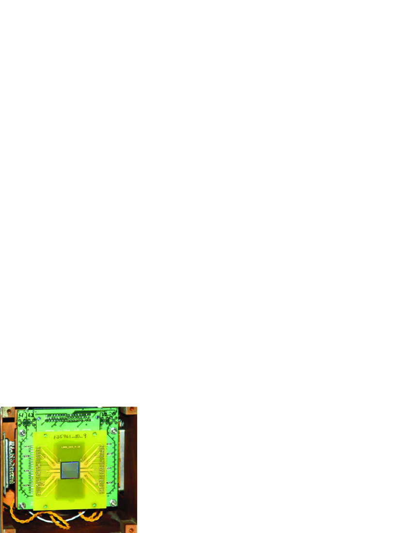
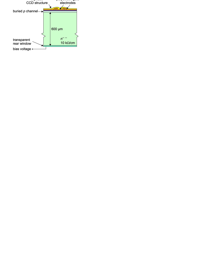
This detector (Fig. 1) was developed by Stephen Holland in Berkeley Laboratory in 2010. It is a p-channel front illuminated CCD fabricated on high-resistivity, n-type silicon. A low density impurities implant in the n-region together with a reverse bias voltage in a ohmic contact in the wafer back side allows to operate the detector with a large fully depleted region increasing the quantum efficiency for infrared light. The resistivity is about 10000 ohm/cm and 40V is a common substrate voltage for the detector. Using this combination, it is possible to obtain a depletion region width around 250 m in comparison with the 20 m of standard detectors [9]. A cross section of the CCD for one pixel is shown in Fig. 2.
The detector is composed by an array of 1022 by 1024 pixels with a pixel width of 15 m. The sensors are grouped in four regions (L1, L2, U1 and U2) which are read by four amplifiers placed in each corner of the chip. The horizontal registers that move the charge to the output stage are placed in two sides of the detector (Fig. 3). Both horizontal and vertical gates are arranged in a three phase configuration [5] where V1, V2 and V3 move the charge vertically, and H1, H2 and H3 transfer it horizontally to the output amplifier. In the output stage the charge is moved by the summing well gate (SG), output gate (OG) and and dump gate (DG) clocks (see Section 2.3).

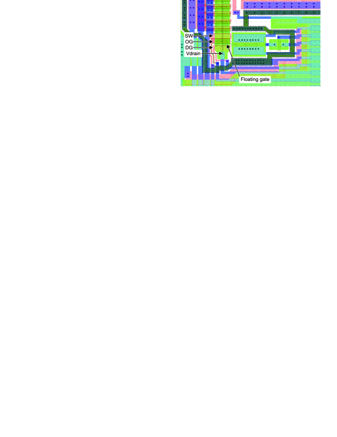
The charge packet is transferred to the sense node, where the output amplifier in a common drain configuration drives the video signal to the readout system. A distinctive feature of the Skipper CCD is its floating gate output stage [6, 8] that allows for non destructive charge measurements, instead of the common floating diffusion output stage used in standards CCDs. The layout of the output stage of the L2 amplifier is shown in Fig. 4.
In the following section the sensitivity of the traditional floating diffusion output stage is compared to the floating gate of the Skipper CCD.
2.1 Floating diffusion output stage
This is the typical output configuration in standards CCDs since it provides the highest sensitivity (voltage increment at the CCD output per hole collected) because the output amplifier gate is connected directly to the CCD p-channel providing a minimum capacitance. When a package of charge is transferred to the floating diffusion node, it produces a voltage , where is the charge packet transferred and is the total capacitance between the node and ground given by
| (1) |
where is the channel-bulk junction capacitance for the sense node region, is the parasitic capacitance between the diffusion and surrounding CCD gates, and is the output transistor input capacitance, which depends on its dimensions and polarization. The signal-to-noise ratio at the output increases with low values, so the effect of the noise in the pixel value is strongly related to [5].
2.2 Floating gate output stage
In this configuration the output transistor gate is connected to the channel through a gate with a silicon oxide insulating layer that provides a stop barrier for holes when they are measured, so the charge remains in the sense node after it is measured [8]. With properly clock timing, the charge can be moved back and forth between the SG region and the sense node, allowing for multiple samples of the same pixel (see next section). The sensitivity becomes a critical aspect of the design because of the extra capacitance added by the floating gate that acts as a capacitive divisor between the sense node and the output transistor gate [5]. In this case the voltage signal at the transistor gate is
| (2) |
where is the new oxide capacitance of the floating gate. The new term in the equivalent capacitance reduces the amplitude of the voltage signal available at the output node. From this equation it seems that increasing is a possible solution for reducing the extra capacitance, but it does not take into account the increase of capacitance as the gate area is increased. In actual designs, is larger than , and smaller gate areas are used to reduce the junction capacitance for a net increase of the sensitivity. However, small gate area reduces the full well capacity (the maximum number of holes handled by the device) so the size of floating gate area results in a trade off between sensitivity and full well capacity.
To explore how this variables are related and its impact on the sensor performance, the Skipper CCD has been designed with different gate areas for each amplifier (L1: 216 m2, L2: 96 m2, U1: 60 m2, U2: 96 m2).
Despite the extra capacitance, the sensitivity observed for our Skipper detector is similar to detectors using floating diffusion configuration, under the same testing conditions. The charge-to-voltage conversion factor was estimated at V [9].
2.3 Skipper operation
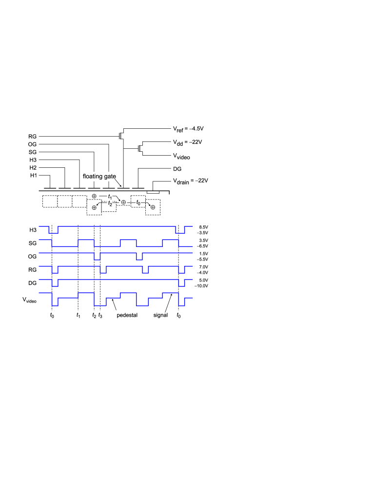
The main advantage of the floating gate output stage of the Skipper CCD is its capability of performing multiple pixel readings with minimum effect on the storage charge. The flow of the charge is controlled by the summing gate clock (SG), output gate clock (OG), and dump gate clock (DG) and the timing of these signals for reading out the same pixel three times are shown in Fig. 5. In the charge package is placed under the last H3 gate at the end of the serial register. The SG clock goes down attracting the charge pocket under its gate. After a few microseconds H3 goes high and the charge remains completely stored under SG. At the same time DG and the reset gate (RG) signals go down to remove the previous pixel charge from the channel and to set the new reference voltage for the current pixel. In the charge is transferred from the SG to the sense node through the OG. The SG is set high increasing its channel potential above the OG barrier so the charge moves to the potential well set by the last reset pulse in the sense node. At this point the charge produces a change in the reference level at the output transistor gate that is reflected as a step increment in the output video signal. The skipper cycle continues when the holes are transferred backward again to the SG in . This process is achieved moving OG and SG to low level. As the SG sets a lower channel potential all the charge goes directly under its surface and the OG acts like a potential barrier to confine the charge, in this case, under the SG. In , after the charge is moved out from the sense node, the RG resets the floating gate to the voltage resulting in a new reference level for the new pixel sample. Using this sequence the pixel value is encoded as the difference of two constant levels. The reference level is called the pedestal level, and the second one the signal level.
By repeating , and cyclically, several measurements of the same pixel can be performed. After reading the desired number of samples, the pixel reading procedure is completed when the charge is removed from the channel and the floating gate is reset by the DG and RG pulse in (of the next pixel), respectively. When DG goes down, it leaves a potential path between the sense node and the ohmic contact for channel discharging.
The key point for the noise reduction algorithm is that the noise is less correlated among samples, and therefore simple averaging can be used for noise reduction.
3 Output noise and readout systems
Regardless of the type of CCD output stage, the pixel measurement is differentially encoded between two constant levels in the video signal, and the amount of charge can be calculated simply by subtracting them. However, as the signal is corrupted by electronic noise originated mainly in the output transistor, more sophisticated readout methods should be used to achieve low RN. There are two different mechanisms that produce signal fluctuation, and each one is characterized by a distinctive power spectrum density (PSD) and a different RN contribution in the pixel value [5, 6]. These noise sources are:
-
•
white (Johnson) noise, caused by random fluctuation of free charges that are part of the transistor current;
-
•
(flicker) noise, caused by traps in the output transistor channel that catch and release moving charge for relatively long periods, producing a noise with more power at low frequencies.
Figure 8 shows the noise PSD (red line) for the CCD video signal. Both noises mechanisms are clearly recognizable: high power components at low frequencies for the noise, and a flat PSD at high frequency as part of the white noise.
The main task of the readout system is to recover the pixel value while rejecting the noise. In the following subsections the readout system for standard and Skipper CCDs are briefly reviewed, and their noise and signal performance are derived.
3.1 Standard CCD readout system
The dual slope integrator (DSI) readout system [10] has been widely used because it provides an optimal filtering for white noise [4]. Instead of taking just one sample of each constant level, the DSI performs an integration during a given time interval of both the pedestal and the signal levels. The pixel charge is obtained as the difference between the results of the integration in both regions.
Using this description it is possible to derive the frequency response of the DSI to analyze the effects of noise in the image pixel. As the pixel value is the difference between the results of the pedestal and signal level integrations, the DSI impulse response is
| (3) |
where is an arbitrary integration gain, is an arbitrary time instant when the pedestal begins, and is the total integration time, reparted equally between the signal and pedestal levels. This model assumes that transients in the video signal from the CCD that occur in the transition between pedestal and signal intervals, and viceversa, and others caused by clock leakages, etc. have been removed. From now on, we consider and for simplicity. Then the module of the frequency response is given by
| (4) |
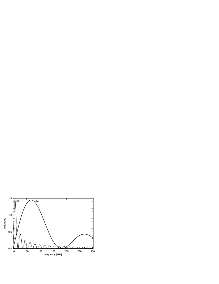
Plots of for two different integration times are shown in Fig. 6. The frequency response for s is plotted as a black dashed curve (a), and for s as a black solid trace (b). When the total integration time is increased, the frequency response curve shifts to a lower frequency band, and its bandwidth decreases, (each lobe gets thinner) reducing the effective bandwidth of the readout system. Therefore, the incidence of white noise on the pixel value is reduced. However, this RN reduction is limited by the noise, because of the shift of the frequency response curve to lower frequencies where the noise PSD is higher.
3.2 Skipper CCD readout system
The multiple readout technique allows to go below the RMS limit given by the noise and get sub-electron RN. After the multiple sampling, the readout system averages the samples for each pixel to get its final value. As each pixel is the average of samples and each sample is read using the DSI technique, the impulse response of the readout system is the linear combination of time shifted copies of :
| (5) |
where
| (6) |
and is the time interval between samples. In this case each pixel is read times during an interval , but the total integration time employed by the readout system for reading one pixel is again . The jumps in the impulse response, alternating between positive and negative levels, causes extra rejection for correlated low frequency components compared to the standard DSI.
Using Fourier transform properties, and assuming for simplicity, the module of the frequency response for the skipper readout system results in
| (7) |
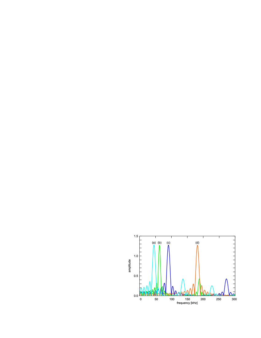
The performance of the Skipper CCD readout system can be explained with the help of Fig. 7. Curves (a)-(d) depict the frequency response of the readout system for different values of and . Curves (a), (c) and (d) correspond to a constant integration time , but increasing number of averaged samples (5, 10, 20, respectivley). As the total integration time remains constant, the bandwidth of each response is approximately the same because it is dominated by the zeros of the . Increasing the number of averages shifts the frequency response moves to higher frequencies, and the gain for low frequencies is reduced.
The curve (b) corresponds to a total integration time s and averages. As the total integration time is increased, the bandwidth is narrower than in the case of s and shown in curve (c); the larger integration time displaces the main lobe to a lower frequency, and the lower number of averages increases the low-frequency gain.
These results show that to achieve maximum performance of the Skipper readout system, 1) a total integration time as large as possible must be used to narrow the bandwidth of the system, and 2) the number of measurements must be chosen to obtain maximum rejection at low frequency and dispace the main lobe of the frequency response to higher frequencies avoiding the limitation. However, it should be clear that the extra RN reduction is paid by an extra readout time, so this should be consider for each aplication.
Although in theory there is no limitation in RN reduction by increasing the number of averaged samples, there is a practical limit imposed by some losses in the charge transfer. However, in our experiments we have not found significant degradation of the signal even when sampling each pixel 1600 times.
Therefore, choosing apropriate values for the total integration time and the number of averaged samples , the Skipper CCD readout system can be adjusted to reject the noise and provide an optimal filtering of white noise because the integration performed over the signal.
3.3 Comparison of DSI and Skipper performance
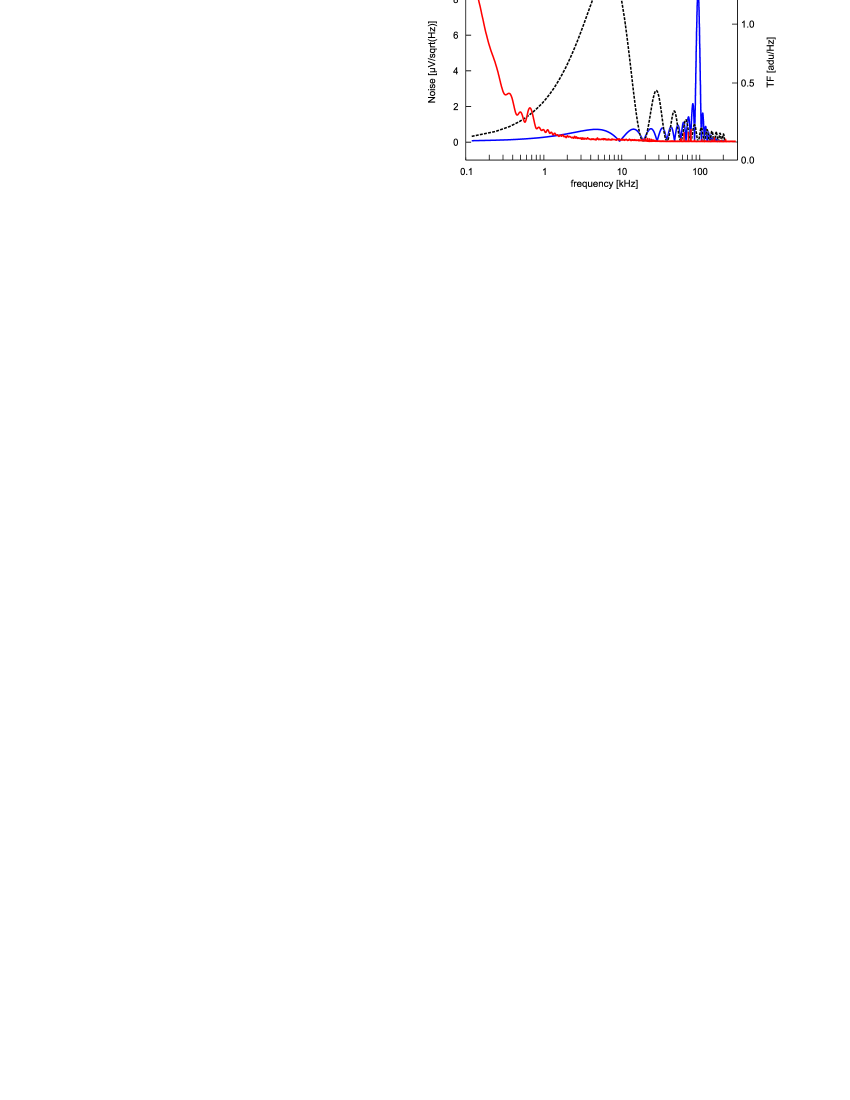
The main advantage of the Skipper readout system is perceived when its frequency response is compared to the standard DSI frequency response for the same time integration interval, i.e., using the same total amount of time for reading each pixel. In Fig. 8 the frequency response of the DSI readout system (curve (b)) is plotted for s, together with the frequency response of Skipper readout system for s, and (curve (c)). These responses are the same as curve (a) in Fig. 6, and curve (c) in Fig. 7, respectively, but plotted using a logarithmic frequency axis. Also in Fig. 8 the PSD of CCD noise is depicted as curve (a). This figure reveals that the Skipper CCD readout system has a higher rejection for high power, low frequency components allowing a RN reduction even in presence of noise, and this rejection can be increased by merely augmenting the number of averaged samples.
In other words, low frequency noise rejection is achieved and the limitation is removed.
4 Experimental results
In this section, the behavior of the noise-reduction technique for the skipper readout system to achieve sub-electron RN levels is analyzed. This extremely low background noise is not only of interest per se, but also of paramount importance in certain applications: we show how this technology can be used to reduce uncertainty in low energy X-ray detection in a controlled X-ray detection experiment.
The readout system utilized in this experiment was originally developed for the DECAM project (Dark Energy Camera, [11]) at Fermilab [12, 13] and it was modified to handle the skipper technology. The detector was tested at one of the Fermilab’s laboratories. The CCD was installed in an aluminum dewar and it was run at ∘K to avoid dark current generation. Each sample was read with an integration time of s and then the total integration time for each pixel is . This integration time does not take into account the duration of the signal to pedestal and pedestal to signal pulses. Therefore, the actual reading time may be a small percentage larger than .
4.1 Background noise measurements
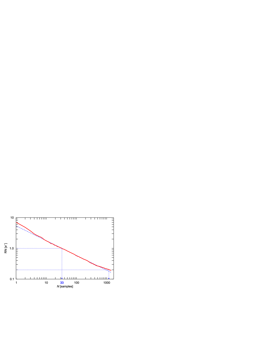
As stated in Section 3.2, the RN level can be reduced by increasing the number of samples taken from each pixel. A series of measurements in the deterctor’s overscan region were performed to measure the background noise of the CCD. This test is useful to determine the number of samples required for obtaining sub-electron RN levels. Figure 9 shows the RMS noise in electrons ( RMS) as a function of the number of samples averaged for each pixel. The continuous line depicts the RN noise measured from the images, and the dashed line is the theoretical white noise reduction fitted for those points. The differences are caused by and other correlated noise components present in the video signal. The figure shows that as the number of averaged samples increases, the measured RN decreases, following the white noise tendency. This effect corroborates the analysis of Section 3.2, revealing that augmenting the number of averaged samples of each pixels increases the rejection of low frequency () noise, and as a result the main noise contribution is given by the white noise component.
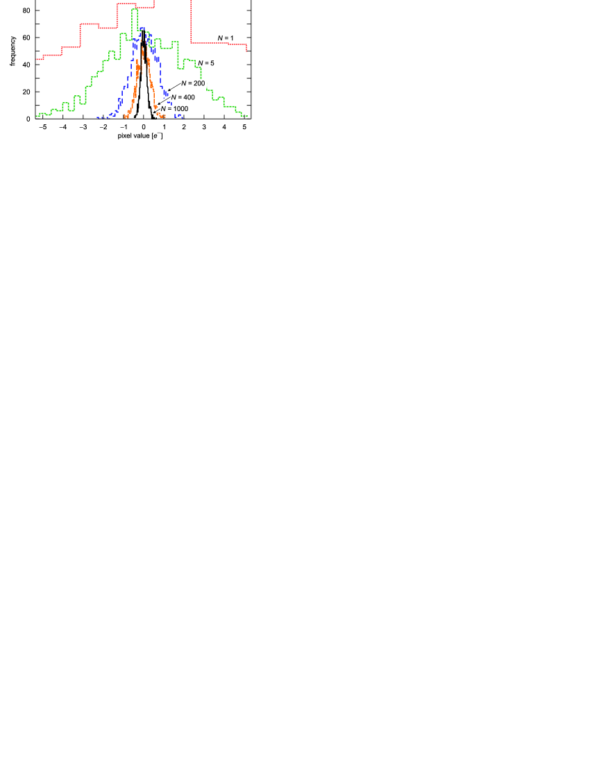
The figure reveals that sub-electron RN can obtained for and a RN = RMS is achieved when averaging samples. The same results are depicted in a more intuitive form using histograms in Fig. 10. The width of the Gaussian distribution is greatly reduced by the averaging of samples, and for all the RN values are practically contained within the RMS segment allowing for very low signal detection. The RN noise level achieved for different number of averaged samples is summarized in Table 1.
| RN [ RMS] | |
|---|---|
| 1 | 7.00 |
| 5 | 2.60 |
| 200 | 0.40 |
| 400 | 0.29 |
| 1400 | 0.19 |
4.2 X-ray experiment
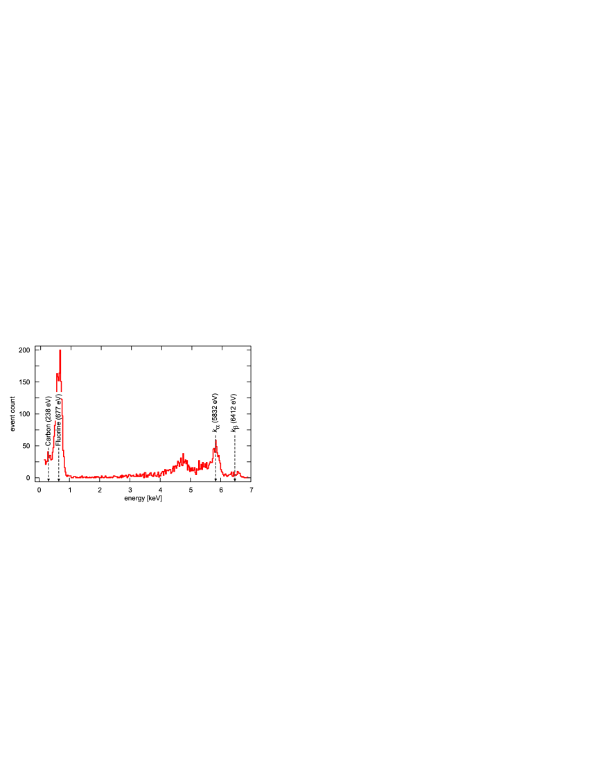
To verify the skipper functionality for low RN applications, it was applied to reduce uncertainty in low-energy X-ray detection in a controlled X-ray detection experiment. Jointly with the detector a Fe55 X-ray source and a teflon target were installed in the dewar. The detector is mounted in front of the target, and this in front of the source. A shielding is placed between the source and the CCD for stopping direct X-rays.
The Fe55 X-ray source produces two different energy rays from Mn: 5832 eV () and 6412 eV (). Both X-rays hit the teflon with carbon and fluorine, which emits lower energy X-ray by fluorescence. Each atom has a precise energy pattern of emitting photons [7]. For the carbon and fluorine the most probable emitted X-rays are at energies of 277 eV and 677 eV, respectively. These low-energy X-rays are detected by the CCD together with some high energy X-rays coming directly from the source that get to cross the shielding. Figure 11 shows the histogram of the X-rays detected by the Skipper CCD. The largest peak is given by the fluorine that is the most common element in the Teflon composition, so it has the most probable interaction. Both spurious peaks of the source are present to a lesser extent at high energies. The small peak at the left of the fluorine peak is the carbon peak, which is pretty small because of the low energy X-rays have very small penetration in the material, so most of them get trapped before leaving the target in the same teflon material (or in the chip layers on the top of the silicon for front-illuminated CCDs). Due to its low noise background, the Skipper CCD multiple-sample technique allows for a much cleaner images and improves the low-energy hit detection.
5 Conclusions
A readout technique for sub-electron noise level measurements was devised for a new type of CCD imager suitable for low background noise applications. This method is based on the capability of the Skipper CCD of admitting several non-destructive measurements of the charge storage in each pixel. The noise and signal characteristics of the proposed readout system are derived, and compared to traditional methods used for typical CCDs (DSI).
Experimental results confirm the expected behavior of the system, and its application to reduce uncertainty in low energy X-ray detection in a controlled X-ray detection experiment reveals the utility of this technique.
It is expected in a near future to update the detector system of the direct dark matter search using CCDs (DAMIC) experiment with this technology [14].
References
- [1] Boyle, W.S.: Nobel Lecture: CCD—An extension of man’s viewRev. Mod. Phys., 82(3), 2305–2306, (2010)
- [2] Smith, G.E.: Nobel Lecture: The invention and early history of the CCD, Rev. Mod. Phys. 82 (3), 2307–2312, (2010)
- [3] Flaugher, B.: The Dark Energy Survey instrument design, in I.S. McLean, M. Iye (eds.) Ground-based and Airborne Instrumentation for Astronomy, Proceedings of the SPIE, 6269, (2006)
- [4] McLean, I.: Electronic Imaging in Astronomy - Detectors and Instrumentation, 2nd ed., Springer-Praxis, Berlin (2008)
- [5] Janesick, J.R.: Scientific Charge Coupled Devices, SPIE Publications, Bellingham, Washington, (2001)
- [6] Chandler, C.E., Bredthauer, R.A., Janesick, J.R., Westphal, J.A., Gunn, J.E.: Sub-electron noise charge coupled devices, SPIE Charge-Coupled Devices and Solid State Optical Sensors 1242, 238–251 (1990)
- [7] Janesick, J.R., Elliot, T., Dingizian, A., Bredthauer, R., Chandles, C., Westphal, J., Gunn, J.: New advancements in charge-coupled device technology: sub-electron noise and 4096x4096 pixel CCDs, SPIE Charge-Coupled Devices and Solid State Optical Sensors 1242, 223–237 (1990)
- [8] Wen, D.D.: Design and Operation of a Floating Gate Amplifier, IEEE Journal of Solid-State Circuits SC-9(6), 410–414 (1974)
- [9] Holland, S.E., Groom, D.E., Palaio, N.P., Stover, R.J., Wei, M.: Fully depleted, back-illuminated charge-coupled devices fabricated on high-resistivity silicon, IEEE Trans. Electron Devices 50(1), 225–238 (2003)
- [10] Wey, H.M., Guggenbuhl, W.: An improved correlated double sampling circuit for low noise charge coupled devices, IEEE Trans. Circuits Syst. 37(12), 1559–1565 (1990)
- [11] Honscheid, K., DePoy, D.L.: The Dark Energy Camera (DECam)-A new instrument for the Dark Energy Survey, IEEE Nuclear Science Symposium Conference Record NSS ’08, 3357–3360 (2008)
- [12] Diehl, H.T., Angstadt, R., Campa, J., CeaseH., Derylo, G., Emes, J.H, Estrada, J., Kubik, D., Flaugher, B.L., Holland, S.E, Jonas, M., Kolbe, W., Krider, J., Kuhlmann, S., Kuk, K., Maiorino, M., Palaio, N., Plazas, A., Roe, N.A., Scarpine, V., Schultz, K., Shaw, T., Spinka, H., Stuermer, W.: Characterization of DECam focal plane detectors, in Dorn, D.A., Holland, D. (eds), High Energy, Optical and Infrared Detectors for Astronomy III, Proceedings of the SPIE, 7021, 70217 (2008)
- [13] Estrada, J., Abbott, T., Angstadt, B., Buckley-Geer, L., Brown, M., Campa, J., Cardiel, L., Cease, H., Flaugher, B., Dawson, K., Derylo, G., Diehl, H.T., Gruenendahl, S., Karliner, I., Merrit, W., Moore, P., Moore, T.C., Roe, N., Scarpine, V., Schmidt, R., Schubnel, M., Shaw, T., Stuermer, W., Thaler, J.: CCD testing and characterization for dark energy survey, in I.S. McLean, M. Iye (eds.) Ground-based and Airborne Instrumentation for Astronomy, Proceedings of the SPIE, 6269, 62693K, (2006)
- [14] Estrada, J., Cease, H., Diehl, T., Flaugher, B., Jones, J., Kibik, D., Sonnenschein, S.: Prospects for a direct dark matter search using high resistivity CCD detectors URL arXiv:0802.2872v3 [hep-ex] (1 Jul 2008) (2008)