Si nanoparticle interfaces in Si/SiO2 solar cell materials
Abstract
Novel solar cell materials consisting of Si nanoparticles embedded in SiO2 layers have been studied using positron annihilation spectroscopy in Doppler broadening mode, and photoluminescence. Two positron-trapping interface states are observed after high temperature annealing at 1100∘C. One of the states is attributed to the (SiO2/Si bulk) interface and the other to the interface between the Si nanoparticles and SiO2. A small reduction in positron trapping into these states is observed after annealing the samples in N2 atmosphere with 5% H2. Enhanced photoluminescence is also observed from the samples following this annealing step.
Solar cell industry has relied on silicon as the mainstream material since the discovery of the Si-based photocell Chapin et al. (1954). The advantages of Si solar cells are unambiguous; they are easy to produce in masses, relatively cheap, can be used in various applications, and Si is non-toxic. However, the energy conversion efficiency is just approaching 25% for the very best commercial Si solar cells, and the typical mainstream cells have efficiencies of around 15% Quick (2010). The classical theoretical limit for single Si solar cells, based on the energy spectrum of the Sun and the band gap of Si, is not much better: 31% Martí and Araújo (1996). A typical way to produce very efficient solar cells is to use composite structures consisting of layers made from different materials sensitive to different wavelengths of sunlight Fraas (1981). These multilayered solar cell structures are, however, very complex to produce and thus expensive so they are not suitable for mainstream use. Since traditional energy sources such as coal and oil are gradually running out and on top of that pollute the Earth’s atmosphere, researchers are very eager to find ways to better harness the energy of the Sun. A promising concept was discovered a couple of years ago when Klimov and his colleagues discovered that silicon nanocrystals could convert a single photon into more than one excitons Schaller and Klimov (2004). A solar cell utilizing this property could be a workaround for getting beyond silicon’s theoretical energy conversion efficiency without having to resort to expensive materials. Promising candidates for such solar cells could be silica layers embedded with Si nanocrystals. Such layers have been prepared and studied with several techniques Cho et al. (2004a, b); Conibeer and et. al. (2006); Hao and et.al. (2009); Osinniy et al. (2009); Zacharias et al. (2002); Surana et al. (2010). The results have been mostly promising but there is still much work to be done before these solar cells can become commercially available. The biggest problem is that the interface between the nanocrystals and silica tends to have carrier traps in it, thus decreasing the light conversion efficiency.
Positron annihilation spectroscopy (PAS) is a versatile tool for studying vacancy-type defects in various materials. Krause-Rehberg and Leipner (1999); Saarinen et al. (1998) The annihilation radiation provides atomic resolution which is useful in getting information about the defects themselves as well as about the atoms in their near vicinity. The use of slow, monoenergetic positrons allows the study of defect distributions in thin layers and interfaces.
In this work, we used a monoenergetic slow positron beam in Doppler broadening mode to study interfaces between silicon nanocrystals and SiO2 which they were embedded in. The fast positrons emitted by a 22Na source were moderated with a 1 m tungsten foil, accelerated with an electric field and then implanted into the sample at energies ranging from 0.5 to 35 keV. After implantation, the positron thermalizes rapidly in the sample; the thermalization time is but a few picoseconds. Following thermalization, the positron diffuses in the sample for 100-250 ps (tens to hundreds of nanometers depending on the material and the defects present) before it finds an electron and annihilates. Saarinen et al. (1998); Krause-Rehberg and Leipner (1999) Positrons can get trapped into neutral and negatively charged open volume defects in the sample. Particularly, open volume defects such as vacancies act as efficient positron traps. Such defects can be characterized by increased positron lifetime in lifetime measurements and a narrower momentum distribution in Doppler broadening measurements.
In positron Doppler broadening spectroscopy, the broadening of the 511 keV annihilation line due to the momentum of the annihilating electron-positron pair is detected. In this work, two high purity Ge detectors with an energy resolution of 1.2 keV at the 511 keV line were used to detect the annihilation quanta and to measure their energies. When a positron annihilates with an electron, two 511 keV annihilation quanta are emitted at almost the opposite directions, with a small angular difference induced as an additional effect of the momentum of the annihilating pair being conserved in the process.
In the standard Doppler broadening measurements, the results are typically described with the conventional line shape parameters and . The parameter, also often referred to as the low momentum parameter, is defined as the fraction of counts in the central part of the annihilation peak. Annihilations contributing to this part of the spectrum correspond mainly to valence electrons. The high momentum parameter , analogously, tells the fraction of counts in both wings of the annihilation peak and corresponds mainly to annihilations with core electrons. The energy windows for both parameters are typically chosen so that the sensitivity of both is at maximum when it comes to changes in the annihilation environment. In this work, the windows were set to pz 0.44 a.u. for and 1.60 a.u. pz 4.10 a.u. for . Open volume defects have a reduced electron density and this narrows the Doppler-broadened spectrum. Thus, an elevated (or lowered ) parameter typically indicates the presence of open volume defects in a sample.
The measured line shape parameters and are always superpositions of the and parameters of different positron states in the sample. In the simplest case, there are only two possible annihilation states (surface and bulk, or bulk and a defect) and the measured parameters can be obtained from
| (1) |
| (2) |
where is the parameter of state and the annihilation fraction in state . The equations above being parameterized equations of lines in the (, ) plane is very useful; plotting the measurement results in the (, ) plane and analyzing the slopes of the aforementioned lines helps in identifying the defects present in the sample. Also, any nonlinear behavior in an (, ) plot is an indication of three or more positron annihilation states. These can be any combination of surface, bulk, defect and other positron trapping states such as interfaces.
Multilayer structures consisting of 30 Si/SiO2 bilayers capped by an SiO2 layer of 50 nm were deposited on oriented p-type Si (100) substrates by using an RF magnetron sputtering system without substrate heating. Si and SiO2 targets were alternately sputtered in Ar gas at 3 mTorr. In the bilayers, the thickness of each SiO2 layer was 4 nm while Si layers of thicknesses of 1, 2 and 4 nm were employed in the three samples named as the 1 nm, 2 nm and 4 nm samples, respectively. Thus, the total thickness of the layer structure was either 200 nm, 230 nm or 290 nm. A pure SiO2 layer of 300 nm used as a reference was also deposited on p-type Si substrate by magnetron sputtering without substrate heating.
In order to form the Si nanocrystals, all samples were annealed in N2 at 1100∘C for one hour. Then each annealed sample was cut into two pieces and one of them was further annealed in 95% N2 + 5% H2 at 500∘C for one hour in order to passivate defects Wilkinson and Elliman (2003); Yedji et al. (2011); Koponen et al. (2009). Positron measurements were then performed on all three types of samples (as-deposited, once annealed and twice annealed). All measurements were done with a slow positron beam in Doppler broadening mode at room temperature. Photoluminescence measurements were also performed on all samples. A continuous wave laser (Oxxius Violet) with a wavelength of 405 nm and excitation power of 50 mW was used as the excitation source. The PL spectra were measured at room temperature using a single monochromator (dispersion 0.8 nm/mm, resolution 0.008 nm) and a silicon photodiode. All spectra were corrected for the spectral response of the detection system.
In Fig. 1, the positron parameter is shown as a function of positron implantation energy for the as-deposited and the two annealed samples with 2 nm Si layers. The layer structure is easily seen in the as-deposited sample as a flat plateau at implantation energies 1-5 keV. This region looks completely different in the sample annealed at 1100∘C. There is a sharp peak at 2 keV and a valley at around 5 keV. Both of these features indicate a decrease in the positron diffusion length L+ which means that positrons get trapped either at the interfaces or in interfacial defects. The second annealing step at 500∘C involving H brings the parameter down which is a sign of reduced positron trapping.
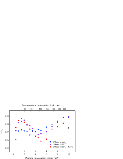
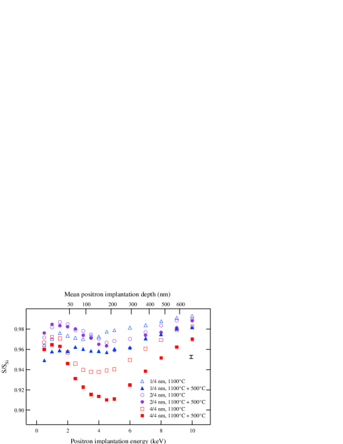
Figure 2 shows how (E) behaves as a function of Si layer thickness in annealed samples. The features mentioned in the previous paragraph are present in all samples but their magnitude is almost negligible in the 1 nm sample. The valley is deepest in the data from the 4 nm sample but the highest peak is actually found in the 2 nm sample. The effect of additional annealing is similar in all samples although the valley at 5 keV deepens considerably more in the 4 nm sample than in the other two.
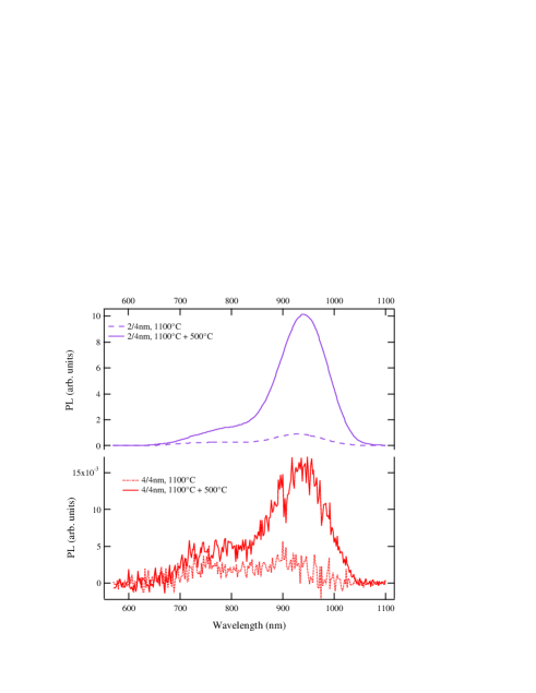
The photoluminescence results shown in Fig. 3 correlate nicely with the positron results. The PL signal from the 2 nm sample is the strongest whereas no photoluminescence at all is observed in the 1 nm sample. The PL peak is positioned at the same wavelength regardless of sample thickness. This indicates that recombination does not occur directly over the band gap as the gap width changes with respect of sample thickness. Thus, the PL signal must come from defects. Furthermore, no PL was observed from the reference SiO2 layer either which means that the defects seen in the PL spectra are located at (SiO2/Si) interfaces and not in the SiO2 matrix.
The positron (, ) parameters of annealed samples are shown in Fig. 4. These results clearly reveal the presence of four different positron states in the samples: the surface (1), two interface states (2 and 3) and the Si substrate (4). The interface numbered 3 in the figure seems to be the (SiO2/Si bulk) interface reported by Kauppinen Kauppinen et al. (1997). Interface 2, however, has unique annihilation parameters which most likely correspond to an unknown defect. Even though the data points coincide with the SiO2 layer reference point in the 1 and 4 nm samples, preliminary coincidence Doppler broadening measurements show that the state seen in these samples does not correspond to SiO2. The signal from the (SiO2/Si bulk) interface is the strongest in the 4 nm sample whereas the unknown interfacial state is most clearly seen in the 2 nm sample.
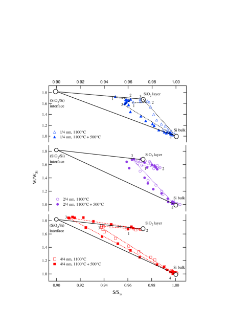
The unknown interfacial state seen at positron implantation energies of roughly 2 keV can be attributed to the interface between the Si nanoparticles and SiO2 in the 2 nm and 4 nm samples. The fact that the positron signal from the nanoparticle interface is the strongest in the 2 nm samples shows that the nanoparticle formation is optimized in that sample. The PL results are in agreement with this observation. At a glance the unknown interfacial state in the 1 nm samples looks similar to the other samples, especially when the (, ) plot of Fig. 4 is considered. However, when looking at the parameter data in Fig. 2, it becomes obvious that the changes in positron diffusion length are much smaller in this sample than in the other two. In fact, the peak at roughly 2 keV looks more like a plateau. This indicates that while positrons get trapped by something also in the 1 nm samples, the trapping state is not the nanoparticle interface. Most likely another positron-trapping structure is formed during the annealing in these samples. No PL is observed from the 1 nm samples so data given by the two techniques are consistent here as well.
The second annealing step slightly reduces positron trapping into the nanoparticle interfaces as seen in Figs. 1 and 2. This can be explained with H atoms filling parts of the open volume at these interfaces. Photoluminescence from the samples – as Fig. 3 shows – increases dramatically following the second annealing step. The interpretation of these two results is that only a small fraction of defects present at the nanoparticle interfaces are actually annealed out during the second annealing step and most are passivated with the help of hydrogen. Thus, it is evident that the H passivation step is successful and H ends up at the interfaces.
The signal from the (SiO2/Si bulk) interface getting stronger as the Si layer thickness increases can be explained with the Makhovian implantation profile of slow positrons Asoka-Kumar and Lynn (1990). The profile is highly asymmetric and widens at high positron implantation energies. This means that in samples where the (SiO2/Si bulk) interface is located deeper (i.e. the ones with thicker Si layers) and is probed with higher implantation energies, a larger fraction of the positrons reaches the interface and annihilates there.
In conclusion, we have studied novel solar cell materials consisting of Si nanoparticles embedded within SiO2. The nanoparticles were formed by annealing Si/SiO2 multilayer structures in N2 at 1100∘C. The samples were studied with positron annihilation spectroscopy and photoluminescence. The nanoparticle formation was shown by both techniques to be the most successful in the sample with 2 nm thick Si layers. A second annealing step at a lower temperature (500∘C) involving H was shown to make defects at or near the nanoparticle interfaces optically passive and thus enable the use of this material as a solar cell.
Financial support from the Danish Council for Independent research | Technology and Production Sciences (FTP) through the SERBINA project is acknowledged.
References
- Chapin et al. (1954) D. Chapin, C. Fuller, and G. Pearson, Journal of Applied Physics 25, 676 (1954).
- Quick (2010) D. Quick, Sunpower claims new solar cell efficiency record of 24.2 percent (2010), URL http://www.gizmag.com/sunpower-corp-solar-cell-efficiency-record/15536.
- Martí and Araújo (1996) A. Martí and M. Araújo, Solid State Technology 43, 203 (1996).
- Fraas (1981) L. M. Fraas, Multilayer photovoltaic solar cell with semiconductor layer at shorting junction interface (1981), URL http://www.freepatentsonline.com/4255211.html.
- Schaller and Klimov (2004) R. D. Schaller and V. I. Klimov, Phys. Rev. Lett. 92, 186601 (2004).
- Cho et al. (2004a) E. Cho, Y. Cho, T. Trupke, R. Corkish, and G. Conibeer, in Proc. 19th European Photovoltaic Solar Energy Conference, Paris (2004a).
- Cho et al. (2004b) E. Cho, Y. Cho, J. Xia, R. Corkish, G. Conibeer, and Y. Huang, in Proc. 14th PVSEC Conf., Bangkok (2004b).
- Conibeer and et. al. (2006) G. Conibeer and et. al., Thin Solid Films 511, 654 (2006).
- Hao and et.al. (2009) X. Hao and et.al., Thin Solid Films 517, 5646 (2009).
- Osinniy et al. (2009) V. Osinniy, S. Lysgaard, V. Kolkovsky, V. Pankratov, and A. Nylandsted Larsen, Nanotechnology 20, 195201 (2009).
- Zacharias et al. (2002) M. Zacharias, J. Heitmann, R. Scholz, U. Kahlere, M. Schmidt, and J. Blasing, Appl. Phys. Lett. 80, 661 (2002).
- Surana et al. (2010) K. Surana, H. Lepage, D. Bellet, G. Le Carval, M. Baudrit, P. Thony, and P. Mur, in Photovoltaic Specialists Conference (PVSC), 35th IEEE (2010).
- Krause-Rehberg and Leipner (1999) R. Krause-Rehberg and H. S. Leipner, Positron Annihilation in Semiconductors (Springer, New York, 1999).
- Saarinen et al. (1998) K. Saarinen, P. Hautojärvi, and C. Corbel, in Identification of Defects in Semiconductors, edited by M. Stavola (Academic Press, San Diego, 1998), vol. 51A, p. 209.
- Wilkinson and Elliman (2003) A. R. Wilkinson and R. G. Elliman, Applied Physics Letters 83, 5512 (2003).
- Yedji et al. (2011) M. Yedji, J. Demarche, G. Terwagne, R. Delamare, D. Flandre, D. Barba, D. Koshel, and G. G. Ross, Journal of Applied Physics 109, 084337 (2011).
- Koponen et al. (2009) L. Koponen, L. O. Tunturivuori, M. J. Puska, and R. M. Nieminen, Phys. Rev. B 79, 235332 (2009).
- Kauppinen et al. (1997) H. Kauppinen, C. Corbel, L. Liszkay, T. Laine, J. Oila, K. Saarinen, P. Hautojärvi, M.-F. Barthe, and G. Blondiaux, J. Phys.: Condens. Matter 9, 10595 (1997).
- Asoka-Kumar and Lynn (1990) P. Asoka-Kumar and K. G. Lynn, Appl. Phys. Lett 57, 1634 (1990).