Large-scale defect accumulations in Czochralski-grown silicon
Abstract
Czochralski-grown silicon crystals were studied by the techniques of the low-angle mid-IR-light scattering and electron-beam-induced current. The large-scale accumulations of electrically-active impurities detected in this material were found to be different in their nature and formation mechanisms from the well-known impurity clouds in a FZ-grown silicon. A classification of the large-scale impurity accumulations in CZ Si is made and point centers constituting them are analyzed in this paper. A model of the large-scale impurity accumulations in CZ-grown Si is also proposed. In addition, the images of the large-scale impurity accumulations obtained by means of the scanning mid-IR-laser microscopy are demonstrated.
1 Introduction
The detection of the large-scale impurity accumulations (LSIAs) with the sizes ranged from several to several tens m in CZ Si by means of the low-angle light scatter (LALS) [1] was reported for the first time in Ref. [2]. It was supposed in that work that LSIAs are analogous in their nature to the oxygen and carbon clouds observed in FZ Si in Ref. [3]. It was shown, however, as a result of the research of Si crystals grown at variable growth rate done by LALS and EBIC that most of LSIAs in CZ Si have a shape close to cylindrical [4] which contradict the cloud model [2]. In the present work, an attempt is made to select different in their nature types of LSIAs in CZ Si and an information about their parameters as well as the influence of different thermal treatments on them is given.
2 Experimental details
Industrial substrates of CZ Si:B studied in this work were grown in the 100 and 111 directions and had the specific resistivity from 1 to 40 cm. The specific resistivity of wafers of CZ Si:P, which were also investigated in the work, were from 2 to 20 cm. The oxygen concentration in the material ranged from 6 1017 to 1018 cm-3, the carbon concentration was less than 1016 cm-3.
The investigation was carried out by LALS and EBIC. CO- and CO2-lasers oscillating at the wavelength of 5.4 and 10.6 m, respectively, were used in LALS to select the scattering by free carrier accumulations [5]. To determine the activation energies () of the centers constituting LSIAs, the temperature dependances of LALS intensity were investigated in the range from 85 to 300 K [6]. A shape of LSIAs was determined from the dependances of the LALS diagrams on the sample orientation with respect to the detection plane. The plasma etching of the sample surface in a special regime before the Schottky barrier creation greatly increased the sensitivity of EBIC to electrically-active defects in crystals [7].
Besides, the images of LSIAs were obtained by means of the scanning mid-IR-laser microscopy in both modes: scanning LALS (SLALS) and optical-beam-induced LALS (OLALS) [8]. The 10.6-m emission of CO2-laser was used as a probe beam, the 0.97-m laser radiation served for excess carrier generation in OLALS.
In the experiments on annealings, wafers were cut into four sections. One of them was not treated, the others were subjected to either isothermal
processes at 600 or 800∘C for 24, 48 and 120 h, respectively, or high-temperature treatments at 965, 1100, 1150, 1200 and 1250∘C for several tens minutes. The treatments of CZ Si:B at C resulted in the formation of a large amount of defects of structure which were revealed by the selective etching (SE). The substrates grown in the 100 direction were subjected to both the former and the latter treatments, while those grown in the 111 direction were treated only in the latter way.
3 CZ Si:B
3.1 Initial samples
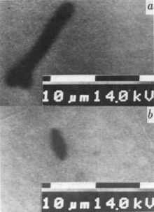
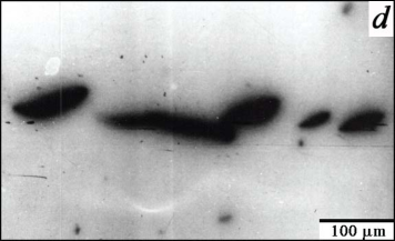
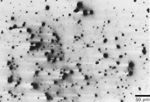
Fig. 1 demonstrates the EBIC images of defects. The samples shown there contain many non-uniformities with the sizes from several to several tens m — mainly cylindrical. In addition, spherical defects are also seen. We have classified the observed defects in the following way.
3.1.1 Cylindrical defects (CDs).
There are sections of LALS diagrams, the shape of which is dependent on the sample orientation to the detection plane (Fig. 4, ). These sections are well fitted with the curves of scattering by cylinders [1] with the diameters from 3–4 to 8–10 m and length from 15 to 40 m depending on a sample. They predominantly oriented along the 110 direction. It is seen from the EBIC patterns that CDs have rather elliptical or curved-cylindrical shape (Fig. 1 ). We assume the CDs revealed by EBIC and LALS to be the same defects similar to CDs observed in Ref. [4].
The concentration of CDs — the most usual defects in CZ Si:B — estimated from EBIC ranged from 106 to 107 cm-3. We could not find a dependance of the CD concentration on oxygen concentration, growth direction, ingot diameter or location on a wafer. Nonetheless we found their concentration to vary within a wafer as well as in different wafers.
LALS measurements at 10.6 and 5.4-m wavelength showed CDs to be domains of the enhanced free carrier concentration [5]. Using the CD concentrations from EBIC, the variations of the dielectric function () and the maximum free carrier concentration in them () were evaluated [1]: they are (1–4) 10-4 and (3–10) 1015 cm-3, respectively. CDs occupy less than 3 % of crystal volume and the total amount of impurities contained in them () is not greater than 3 1014 cm-3.
LALS temperature dependances showed for CDs a small (2 to 3 times) drop of the scattering intensity () at about 90 K (Fig. 4, curve 1). This allows us to state that LALS by CDs at 300 K at 10.6 m is controlled by the centers with 40–60 meV containing in CDs. Naturally another defects, such as deep or compensating centers as well as precipitates, inclusions and structural imperfections can also be contained in CDs.
3.1.2 Spherical defects (SDs).
Besides the above sections of LALS diagrams, those independent of the sample orientation were also observed (Fig. 4, ). These sections are well fitted with the curves of light scattering by spherical defects with the Gaussian profile of [1]


and sizes from 5–8 to 20 m. Such defects are also seen in the EBIC pictures (Fig. 1 ). Their concentration is usually about 105 cm-3, (1–3) 10-3, (3–9) 1016 cm-3 [1]. SDs occupy less than 0.04 % of the crystal volume, cm-3.
LALS temperature dependances showed SDs, like CDs, to be domains with enhanced concentration of ionized at 300 K impurities with 120–160 meV. These impurities are “frozen out” at about 250 K, so SD-related scattering is smothered in the range from 90 to 250 K which enables the accurate selection of CD-related scattering in LALS diagrams (Fig. 4).
3.1.3 Superlarge (SLDs) and small (SmDs) defects.
The sections of LALS diagrams well approximated with the curves of light scattering by defects with the sizes greater than 50 m were sometimes observed. SLDs were sometimes seen in the EBIC photographs (Fig. 1 ). These defects appeared to have an asymmetrical shape.
The sections of LALS diagrams independent of the scattering angle (“plateaux”) were often observed at 5.4 m (and sometimes at 10.6 m) which correspond to defects with the sizes less than 4–5 m. for SmDs was also independent of the probe wavelength, so they are domains with the enhanced free carrier concentration. SmDs were sometimes observed in the EBIC picture as well. Although we could not unambiguously determine their shape, SmDs seem to be very small CDs and SDs rather than a separate class of defects. This was verified
by LALS temperature dependances: SmDs were “frozen out” at 90 K when CDs predominated and at 250 K if SDs predominated.
3.2 Annealed samples
The LALS diagrams and EBIC pictures for the annealed crystals did not differ in general features from those for the as-grown samples. The following peculiarities may be emphasized.
1. In crystals annealed in the temperature range of 600–1100∘C, the light scatter by SDs was greatly (but not completely) suppressed, and CDs and SmDs predominated. EBIC showed mainly CDs and SmDs too.
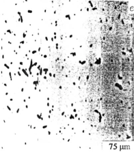
2. Annealing at C resulted in predominance of SD-related scattering and general growth of . A great number of SDs was observed by EBIC (Fig. 5).
3. After annealing at C, the centers with the same as in the as-grown samples composed LSIAs ( 120–160 meV).
4. Annealing at 800∘C and short (up to 48 h) treatment at 600∘C did not change of the centers composing CDs and SDs. Longer treatment at 600∘C resulted in prevailing of the centers with 70–90 meV in CDs and SDs.
5. After 120-h annealing at 600 and 800∘C, SLDs became more habitual than in the as-grown samples. The centers with 130–170 meV were contained in SLDs.
4 CZ Si:P
The data for CZ Si:P are much less complete than those for CZ Si:B. This material was investigated only by LALS. The main results for CZ Si:P can be summarized as follows.
1. The mid-IR-light scattering intensity by the as-grown samples was as a rule rather low, it was in excess of 2 orders of magnitude weaker than that for CZ Si:B 444The similar regularity was observed for FZ Si in passing from -type to -type material [2].. Usual shape of the LALS diagrams was “plateau” which corresponds to the scattering by defects with the sizes less than 4 m, although the diagrams typical for the CZ Si:B crystals reported above were observed sometimes too. These crystals showed the standard for CZ Si:B mid-IR-light scattering intensity and set of defects.
2. Annealings at moderate temperatures (C) resulted in manifestation of the same set of defects that is characteristic for the CZ Si:B crystals. General growth of the mid-IR-light scattering intensity was also observed 555It should be mentioned that as well as the defect size as a function of the annealing temperature is very non-monotonic and consists of a set of maxima and minima [3]. This behaviour is common for both boron and phosphorus doped materials and very different from that in FZ Si where routine diffusion process takes place [2]..
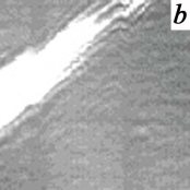
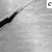
5 SLALS and OLALS images
Recently, a technique of the scanning mid-IR-laser microscopy has been proposed by us for LSDA and LSRD visualization in semiconductors [8]. As it is based on LALS, we use the titles “scanning LALS (SLALS)” and “optical-beam-induced LALS (OLALS)” for its two main modes which are designed for the investigation of LSDAs and LSRDs, respectively.
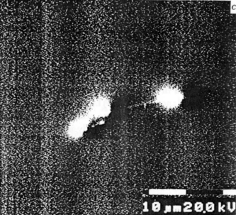
The measurements made by this technique have shown a good agreement with our former observations made by EBIC, so the estimates of the parameters of defects made using EBIC and given above were confirmed by the direct method. Fig. 6 demonstrates pictures of defects in CZ Si crystals measured by SLALS and OLALS.
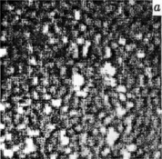
A great number of LSDAs were observed in CZ Si:P with cm which was related to the group of samples with high and a set of defects registered by LALS analogous to that in CZ Si:B (Fig. 6 , white spots are the images of defects). Unfortunately, now we cannot judge about the defects sizes and shapes from SLALS images, as the resolution of the instrument we use at present is two bad [8], but at least the defect concentrations can be evaluated.
Fig. 6 demonstrates the SLALS and OLALS images of a defect which looks like SLD (or a group of SLDs) and is very similar to the image of a group of SLDs shown in Fig. 1 . This picture was obtained from the boundary region between and zones in CZ Si:B crystal with cm, i.e. in the conditions analogous to those in which SLDs usually were observed.
6 Discussion
It is difficult now to determine the nature of LSIAs in CZ Si:B unambiguously. Ii is clear, however, that CDs are domains with the enhanced free carrier concentration caused by point centers with 40–60 meV. CDs look like the defects observed by EBIC after oxidizing annealings [9]. Our research gave an evidence to the presence of these defects in initial crystals, moreover the CD-related sections of LALS diagrams do not change after high-temperature annealings. In our opinion, however, CDs are the impurity atmospheres (IAs) around some defects-precursors, e.g. stacking faults (SFs). Remark that some authors connect the contrast of EBIC patterns with the formation of precipitate colonies around SFs [9]. As these colonies may have no influence on the free carrier concentration in IAs, the following scenario might be proposed.
In initial wafers, the precipitate concentration in IAs is low. At the same time, the dissolved ionized impurity concentration is high enough but insufficient for the precipitate formation, hence is high and the recombination contrast in EBIC is low. During high-temperature annealing, precipitate colonies arise in CDs but the dissolved impurity () and free carrier () concentrations change weakly (e.g. because the impurity concentration in CDs in the as-grown samples was close to the saturation limit or due to the growth of the compensation degree). The recombination contrast will have grown and will have changed weakly and randomly.
From the other hand, the enhanced EBIC contrast may be caused by the specificity of the sample preparation. Two variants are possible. The centers enhancing the EBIC contrast may arise as a result of the plasma etching applied. Alternatively, an “exhaustion” of CDs may be a result of the chemical etching usually applied for sample preparation for EBIC.
Thus, the hypothesis according to which CDs are IAs around SFs does not meet contradictions. As to the point defects composing CDs, we suppose them to be the “new” thermal donors [10] whose activation energies are close to the estimates made 666Although, some alternatives exist [11], and B and [Cu–O] are among them.. The influence of annealing at 600∘C on the activation energy of the centers composing CDs indirectly verifies the assumption 777The growth of ionization energy of “new” thermal donors as a result of long-term annealing at 650∘C was reported in Ref. [12].. New experiments are required to obtain more evidences to the model proposed, though.
SDs also are domains with the enhanced dissolved impurity and free carrier concentrations. We assume SDs to be IAs around defects of structure (e.g. precipitates). This hypothesis is confirmed by the growth of the SD concentration during the high-temperature annealings and correlation with the appearance of structural defects revealed by SE. This assumption also have no sufficient evidences 111Some alternatives to the assumption — the cloud models — are discussed in Ref. [11]. and require an additional research, however.
Some more definite assumption can be made for the centers composing SDs. It was supposed in Ref. [13] that SDs likely contain the centers with the negative correlation energy. Regarding annealing at 600∘C resulting in predominance of the centers with changed in SDs, we assume that, like in CDs, double thermal donors are contained in SDs 888Possible alternatives to these centers are discussed in Ref. [11], they are Bi, [O–V], [Ci–Cs], etc..
SmDs are likely very small CDs and SDs. The nature of SLDs is hard to be discussed now. It is evident only that they are domains with the enhanced concentration of the free carrier and dissolved impurities.
7 Conclusion
On the basis of the above we can summarize in the conclusion that at least two types of LSIAs different in their nature and composition exist in CZ Si:B. Their parameters determined for the group of crystals investigated in this work are rather typical for the industrial Si:B with the specific resistivity from several to several tens cm.
References
-
[1]
V. V. Voronkov, G. I. Voronkova, B. V. Zubov et alSov. Phys.– Solid State 23 (1) (1981) 65–75
V. P. Kalinushkin Proc. Inst. Gen. Phys. Acad. Sci. USSR vol. 4 Laser Methods for Defect Investigations in Semiconductors and Dielectrics (New York: Nova) (1988) 1–79 -
[2]
V. V. Voronkov, G. I. Voronkova, V. P. Kalinushkin et alSov. Phys.– Semicond. 17 (12) (1983) 2137–2142
T. Nazarov Cand. Sci. Dissertation (Tashkent: Tashkent State University) (1986) - [3] V. V. Voronkov, G. I. Voronkova, B. V. Zubov et alSov. Phys.– Semicond. 13 (5) (1979) 846–854
- [4] A. N. Buzynin, S. E. Zabolotskiy, V. P. Kalinushkin et alSov. Phys.– Semicond. 24 (2) (1990) 264–270
- [5] V. P. Kalinushkin, V. I. Masychev, T. M. Murina et alJourn. Tech. Phys. Letters 12 (3) (1986) 129–133
-
[6]
S. E. Zabolotskiy, V. P. Kalinushkin, D. I. Murin et alSov. Phys.– Semicond. 21 (8) (1987) 1364–1368
V. P. Kalinushkin, V. A. Yuryev, D. A. Murin and M. G. Ploppa M G Semicond. Sci. Technol. 7 (1992) A255–A262
V. P. Kalinushkin, V. A. Yuryev and D. I. Murin Sov. Phys.– Semicond. 25 (5) (1991) 798–806 - [7] A. N. Buzynin, N. A. Butylkina, A. E. Lukyanov et alBul. Acad. Sci. USSR. Phys. Ser. 52 (7) (1988) 1387–1390
-
[8]
O. V. Astafiev, V. P. Kalinushkin and V. A. Yuryev
Proc. Soc. Photo-Opt. Instrum. Eng. 2332
(1994) 138–145
O. V. Astafiev, V. P. Kalinushkin and V. A. Yuryev Mater. Sci. Eng. B 34 (1995) 124–131
O. V. Astafiev, V. P. Kalinushkin and V. A. Yuryev Inst. Phys. Conf. Ser. 146 (1995) 775–780
O. V. Astafiev, V. P. Kalinushkin, V. A. Yuryev, A. N. Buzynin and N. I. Bletskan Mater. Res. Soc. Symp. Proc. Vol. 378 (1995) 615–620
O. V. Astafiev, V. P. Kalinushkin and V. A. Yuryev Russian Microelectronics 25 (1) (1996) 41–53
O. V. Astafiev, V. P. Kalinushkin and V. A. Yuryev Inst. Phys. Conf. Ser. 149 (1996) 361–366 - [9] K. Schmalz, F.-G. Kirscht, S. Niese et alPhys. Status Solidi(a) 89 (1985) 389–395
- [10] A. Bouret Proc. 13n Int. Conf. on Defects in Semiconductors ed. L. C. Kimerling (1985) 129–134
-
[11]
O. V. Astafiev, A. N. Buzunin, A. I. Buvaltsev et alSemicond. 28 (3) (1994) 407–415
V. P. Kalinushkin, A. N. Buzynin, V. A. Yuryev et alInst. Phys. Conf. Ser. 149 (1996) 219–224 -
[12]
A. Kanamori and M. Kanamori J. Appl. Phys.50 (1979) 8095–8101
M. Tajima, A. Kanamori and S. Kishino Japan. J. Appl. Phys.19 (1980) L755–L758
K. Yasutake, M. Umeno, H. Kawabe et alJapan. J. Appl. Phys.19 (1980) L544–L546 -
[13]
K. A. Valiev, L. B. Velikov, V. P. Kalinushkin et alSov.
Phys.– Microelectronics 19 (5) (1990) 453–459
D. E. Abdurahimov, P. M. Bochikashvily, V. L. Vereschagin et alRussian Microelectronics 21 (1) (1992) 21–27
LARGE-SCALE DEFECT ACCUMULATIONS
IN CZOCHRALSKI GROWN SILICON
V. P. Kalinushkin, A. N. Buzynin, V. A. Yuryev, and O. V. Astafiev
General Physics Institute of RAS, 38, Vavilov Street, Moscow,
117942, GSP–1, Russia
Tel./Fax: 7 (095) 135 13 30
E-mail: vkalin@ldpm.gpi.ru
It was reported in Ref. [1] about detecting of the large-scale electrically active defect accumulations (LSDAs) in CZ Si. In this work, the data on their nature are presented.
The method of low-angle light scattering (LALS)2 including scanning LALS (SLALS)3, EBIC and selective etching have been used in the experiments. The crystals grown under different conditions and subjected to different treatments have been studied.
It has been shown that CZ Si crystals contain the following types of LSDAs:
-
1.
Cylindrical defects range by diameters from 3–4 to 8–10 m and by lengths from 10 to 40m. They line up with crystallographic directions. Their concentration makes up to 10cm-3, the free carrier concentration in them is (1–10)1015 cm-3. The centers with activation energy of 40–60 meV — presumably “new thermal donors”— form them.
-
2.
Spherical defects have the radii up to 15 m. Their concentration ranges within 104–105 cm-3. They are composed by point centers with activation energy of 130–170 meV. These centers are likely metastable ones with negative correlation energy, probably, oxygen–vacancy complexes and double thermal donors. The free carrier concentration in these LSDAs is (5–50)1015 cm-3.
-
3.
Superlarge defects are those of intricate shape with the sizes greater than 50 m. They have been observed most often in silicon obtained in “vacancy-rich” regime of growth. The nature of these defects has not been found out yet.
-
4.
The crystals of CZ Si contain also a large number of small defects with the sizes less than 2–3 m. At present, their detailed investigation is difficult because of limitations imposed on LALS and EBIC. It may be supposed, however, that at least in a number of cases they are spherical or cylindrical defects of very small dimensions.
A. N. Buzynin et al, Sov. Phys.–Semicond. 24 (1990) No 2.
V. P. Kalinushkin, Proc. Inst. Gen. Phys. Acad. Sci. USSR, Vol. 4, New York, Nova, 1988, p.1.
O. V. Astafiev et al, Proc. SPIE 2332 (1994) 138.