Optical beam-induced scattering mode of mid-IR laser microscopy: a method for defect investigation in near-surface and near-interface regions of bulk semiconductors
Abstract
This paper presents a new technique of optical beam-induced scattering of mid-IR-laser radiation, which is a special mode of the recently developed scanning mid-IR-laser microscopy. The technique in its present form is designed for investigation of large-scale recombination-active defects in near-surface and near-interface regions of semiconductor wafers. However, it can be easily modified for the defect investigations in the crystal bulk. Being in many respects analogous to EBIC, the present technique has some indisputable advantages, which enable its application for both non-destructive laboratory investigations and quality monitoring in the industry.
1 Introduction
A method of low-angle mid-IR-light scattering (LALS) in combination with current carrier photoexcitation in the studied sample has been used for the investigation of large-scale centers of recombination and gluing in the bulk of semiconducting materials for many years [1]. This method has not been applied to the investigation of these defects in near-surface layers of semiconductors until recently, however, although it is evidently promising for both the investigation of near-surface and near-interface regions of semiconducting materials and the inspection of “working” layers of technological semiconductor wafers as well as the studies of large-scale recombination-active defects (LSRDs) directly in “working” layers of semiconductor substrates: in contrast to e.g. SEM in the EBIC mode, it requires practically no special preparation of substrate surfaces and consequently affects the physical properties of neither the studied near-surface layers nor the investigated defects 333The only requirement imposed by this method upon a substrate — polishing on both sides, while a considerable part of technological substrates is polished on one side — seem to be removed by use of the methods of the laser heterodyne microscopy [2].; the method allows one to investigate the interfaces of semiconductors as well as the surfaces covered with dielectric coatings (without coating removing, until the substrate is metallized) that, as far as we know, impossible to do using any of presently existing methods of material investigation and diagnostics. Nevertheless the first works demonstrating the applicability of LALS with surface photoexcitation to investigation of LSRDs in near-surface regions of semiconductors using Ge single crystals as an example were made by us very recently [3]. A method for visualization of LSRDs presented in the current paper — the optical beam-induced scanning low-angle mid-IR-light scattering technique (OLALS) — has become a direct logical development of these works [4]. A scanning dark-field mid-IR-laser microscope (scanning LALS or SLALS) recently proposed for the investigation of the large-scale electrically-active defect accumulations (LSDAs) in semiconductors [5–8] was applied in this technique as a basic instrument.
2 Experimental details
2.1 Optical diagram
An ideal optical diagram of the SLALS microscope in the OLALS mode (Fig. 1) gives a sufficiently clear idea of the instrument used in the present work. Note only the 55-mW He-Ne laser oscillating at the wavelength of 633 nm was applied as a light source for the “surface” photoexcitation of the studied samples, the modulated emission of which was focussed on the sample surface in the back focus of the lens L1 in the spot with the dimensions of around 50 m. The imperfection of the optical and mechanical parts of the laboratory prototype we used impeded us to reach the optimal focusing of the exciting beam 444The microscope resolution in the OLALS mode is controlled by the effective dimensions of the domain, in which the non-equilibrium carrier exist, i.e. at the optimal focusing of the exciting beam the sizes of the light spot must be as small as possible and not exceed several m. The effective dimensions of the non-equilibrium carrier domain — and the resolution — must be controlled only by the carrier lifetime, diffusion coefficient and the surface recombination velocity (we mean materials with s lifetimes). In addition, the SLALS microscope itself imposes some restrictions on the sizes of the scattering domain —the domain of non-equilibrium carriers. Due to spacial filtering applied it depresses the images of too large objects [7, 8].. Nonetheless even the available rather imperfect instrument allowed us to obtain the images of LSRDs in near-surface layers of silicon wafers and demonstrate the serviceability of the proposed technique.
10.6-m CO2-laser emission was used as a probe beam to produce a scattered wave. A liquid nitrogen cooled MCT photoresistor was used as an IR detector.
To obtain images of LSRDs we used the lock-in detection at the modulation frequency of the Ne-Ne laser emission (the probe CO2-laser radiation was not
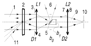
modulated in the OLALS mode), while the lock-in detection at the frequency of the CO2-laser light modulation was applied to obtain images of the same regions of the wafers without photoexcitation (in the basic mode of the SLALS microscope).
2.2 Samples
76-mm 38115 m thick wafers of single crystalline FZ n-Si:P grown in the 100 direction were used as experimental samples. Their specific resistivity ranged from 16 to 24 m. The samples were chemical-mechanically polished on one side by the manufacturer (“Wacker”), the other side of the samples was mechanically polished up to the optical precision grade at GPI of RAS. In addition, we studied a sample of 76-mm CZ n-Si:P grown in the 100 direction (type KEF–4.5) on one side of which 1200 Å thick SiO2 layer was produced by oxidation process (this sample was taken from the CCD matrix production cycle). The opposite side of this sample was polished mechanically up to the optical precision grade.
3 OLALS images
3.1 LSRDs in subsurface region
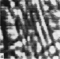
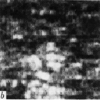
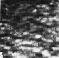
Fig. 2 presents an OLALS image of the subsurface layer of chemical-mechanically polished side of one of the wafers. The same region scanned without photoexcitation (SLALS image) is given in Fig. 2 . The average signal level in Fig. 2 is 5–7 times greater than that in Fig. 2 . The image contrast in Fig. 2 — white spots — is determined by LSDAs in the crystal bulk (these defects were studied by LALS e.g. in [1, 9]), while the contrast in Fig. 2 — dark objects — is caused by domains with the enhanced recombination rate in the near-surface layer of the wafer, i.e. LSRDs. It is seen that most of these LSRD-rich domains look like traces of scratches but no scratches were observed on this side of the wafer by conventional methods.
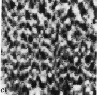
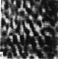
Fig. 2 shows an OLALS image of the opposite — mechanically polished side — of the same wafer, and Fig. 2 presents an image of the same region as Fig. 2 in the SLALS mode. The average signal levels in Figs. 2 and 2 practically equal, while that in Fig. 2 is 10–15 times lower than in Figs. 2 and 2 . A chaotic conglomeration of small LSDAs is seen in Fig. 2 in the damaged by mechanical polishing subsurface layer.
As it should be expected, absolutely different LSRD-rich domains were observed on the wafer sides subjected to different polish processes.
Note that similar inferences were previously made by us from the experiments on LALS with surface photoexcitation of Ge samples [3]. The difference of the data presented in Ref. [3] from the results of this work consists in the following: the big stripe-like LSRDs observed in the present work on the sample side subjected to chemical-mechanical polish cannot be revealed from the light-scattering diagrams in LALS. That is why only defects similar to impurity clouds [1, 9] were observed in Ref. [3] (as it was established in Ref. [3], the latter are also LSRDs). On the mechanically polished side of the samples, like in the present work, rather intense light scatter by small LSRDs was registered in the near-surface layer [3].
Remark also that different schemes of elecron–hole pairs were used in the present work and in the work [3]. In the current work, as mentioned above, the non-equilibrium carriers in the near-surface layer were excited by the focussed light beam in a quasi-continuous regime, and a whole domain of the non-equilibrium carriers scattered light, while in [3], the photoexcitation was produced with a wide light beam in a pulse regime and a surface inhomogeneity in the distribution of non-equlibrium carrier
concentration inside the sight spot caused by subsurface LSRDs was a source of the mid-IR-light scatter. In both cases, the light scatter intensity must be proportional to the square of the non-equilibrium carrier concentration and, in case of linear recombination, the square of the photoexcitation power. The real excitation power dependances will be discussed below.
3.2 LSRDs under SiO2 layer
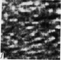
Fig. 2 presents an OLALS image of the silicon wafer surface under the oxide layer. The dark spots in the image represent the domains with low non-equilibrium carrier lifetime 555The closely spaced parallel stripes are the noises brought in the picture by the scanner mechanics.. As far as we know, such defects of a near-interface semiconductor layer directly under the oxide layer have never been observed thus far. It is clear that such a strong nonuniformity of recombination properties of the subinterface layer must disastrously affect the quality of devices, in particular CCD matrices, from the production cycle of which the studied sample was taken. It is obvious also that these defects arose due to wafer processing before the oxidation.
3.3 OLALS signal dependence on photoexcitation power
Fig. 3 demonstrates the dependencies of the scattered CO2-laser light intensity registered by the detector on the power of He-Ne laser radiation absorbed by the crystal for the FZ Si:P wafer sides subjected to chemical-mechanical (1) and mechanical polish processes, OLALS images of which are shown in Fig. 2. The square dependence obtained for chemical-mechanically polished side verifies the fact that this surface is imaged in the rays scattered by the non-equilibrium carrier domain and the recombination is linear 666It is generally known that the light scattering intensity is proportional to the square of the dielectric constant deviation in the scatterer.. The situation is much more sophisticated for the mechanically polished side, for which the cubic dependence was obtained.

The similar dependence was previously obtained by us for the mechanically lapped surface of the Ge sample in Ref. [3]. As of now, we have got no perspicuous explanation for these dependances. Perhaps the cubic dependence is conditioned by the recombination processes in the vicinity of a huge amount of potential barriers in the damaged by mechanical polish subsurface layer of the samples [10]. It is obvious, though, that in this case the surface image is also formed in the rays scattered by the non-equilibrium carrier domain.
4 Conclusion
Summarizing the above we can conclude that this work presents an optical non-destructive technique which can be a powerful tool for the investigation of near-surface and near-interface layers of semiconducting materials. The described method is in some respects analogous in its physics to EBIC or OBIC but as distinct to the latter ones, it requires neither special preparation of a sample surface nor Schottky barrier or p–n junction. It enables the investigation of semiconductor interfaces and surfaces coated with dielectric layers and does not require to remove the coatings.
To demonstrate the method potentialities, the images of LSRDs situated in the vicinity of the chemical-mechanically and mechanically polished surfaces of single crystalline silicon were obtained without preliminary preparation of the surfaces. The images of LSRDs located near the surface, on which the SiO2 layer was created by the industrial process of oxidation, were also obtained without removing the coating and surface processing. As far as we know, such images can be obtained by means of no presently used methods of microscopy. The defects observed on the Si crystal side subjected to chemical-mechanical polish and under the oxide layer, caused by the technological treatments of the wafers, undoubtedly must disastrously affect the serviceability of devices fabricated of such wafers.
We should remark in the conclusion that the technique described is
easily adaptable for work directly in the technological line of
semiconductor devices production and can serve as a promising tool
e.g. for monitoring of the “working” layer quality. Some potential
industrial applications of the technique are disused in Refs. [6, 8].
References
-
[1]
Zubov B V, Kalinushkin V P, Krynetsky B B et al1974
JETP Letters 20 (3) 167–71
Voronkov V V, Murina T M, Voronkova G I et al1978 Sov. Phys.– Solid State 20 (5) 1365–8
Kalinushkin V P, Murin D I, Murina T M et al1986 Sov. Phys.– Microelectronics 15 (6) 523–7
Kalinushkin V P 1988 Proc. Inst. Gen. Phys Acad Sci USSR vol 4 Laser Methods of Defect Investigations in Semiconductors and Dielectrics (New York: Nova) pp 1–79 - [2] Protopopov V V and Ustinov N D 1985 Laser Heterodyning (Moscow: Nauka)
-
[3]
Kalinushkin V P, Murin D I, Yuryev V A, Astafiev O V and Buvaltsev A I 1994 Proc. SPIE 2332 146–53
Astafiev O V, Buvaltsev A I, Kalinushkin V P, Murin D I and Yuryev V A 1995 Phys. Chem. Mech. Surf. (4) 79–83 - [4] Astafiev O V, Kalinushkin V P and Yuryev V A 1995 Journ. Tech. Phys. Letters 21 (11) 52–60
-
[5]
Astafiev O V, Kalinushkin V P and Yuryev V A 1994
Proc. SPIE 2332 138–45;
1995 Mater. Sci. Eng. B 33 in press;
1995 Proc. 9th Int. Conf. on Microscopy of Semiconducting Materials,
Oxford, 20–23 March 1995 (IOP Conf. Ser.) in press
Yuryev V A, Kalinushkin V P and Astafiev O V 1995 Semiconductors 29 (3) 455-8 - [6] Astafiev O V, Kalinushkin V P, Yuryev V A et al 1995 Proc. 1995 MRS Spring Meeting vol 378 ed S Ashok, J Chevallier et al (Pittsburgh: Material Research Soc.) in press
- [7] Astafiev O V, Kalinushkin V P and Yuryev V A 1996 Microelectronics 25 in press
- [8] Kalinuhkin V P, Yuryev V A and Astafiev O V 1995 Proc. 1st Int. Conf. on Materials for Microelectronics, Barcelona, 17–19 October 1994 (Mater. Sci. Technol. 11) in press
-
[9]
Voronkov V V, Voronkova G I, Golovina V N et al1981 J. Cryst. Growth
52 939–42
Zabolotsky S E, Kalinushkin V P, Murina T M, Ploppa M G and Tempelhoff K 1985 Phys. Status Solidi(a) 88 539–42 - [10] Zegrya G G and Kharchenko V A 1992 JETP 101 (1) 327–43