Influence of photoexcitation depth on luminescence spectra of bulk GaAs single crystals: application to defect structure characterization
Abstract
The results of investigation of bulk GaAs photoluminescence are presented taken from near-surface layers of different thicknesses using for excitation the light with the wavelengths which are close but some greater than the excitonic absorption resonances (so-called “bulk” photoexcitation). Only the excitonic and band-edge luminescence is seen under the interband excitation, while under the “bulk” excitation, the spectra are much more informative. The interband excited spectra of all the samples investigated in the present work are practically identical, whereas the bulk excited PL spectra are different for different samples and excitation depths and provide the information on the deep-level point defect composition of the bulk materials.
1 Surface and quasi-bulk photoexcitation: two approaches to luminescence characterization of semiconductors
Photoluminescence (PL) technique is a powerful tool for the investigation of defects in semiconducting materials. In most cases, the luminescence of semiconductors is investigated under the interband excitation, so that electrons are excited from the valence band to the conduction band. After the excitation, the electrons and holes thermalize to the thermoequilibrium distribution in the conduction and valence bands due to electron–phonon and electron–electron (hole–hole) interactions in a time less than 0.1 ps for the holes in the valence band and of about 1 ps for the electrons in the conduction band [1, 2], and then recombine. Main channels of the radiative recombination in semiconductors are the following: free and bound exciton luminescence, band-edge PL involving shallow acceptor-like defects, and luminescence via the states of the deep-level defects or the defect associations. All three types of the PL yield the information on the defect structure of semiconductors.
1.1 Do PL measurements show real deep-level defect structure at band-to-band excitation?
In case of the interband excitation , the exciting light is absorbed in the region less than 0.1 m close to the surface. For this reason, the spectra of the observed luminescence reflect mainly the defect structure of the near-surface layer but not of the sample bulk, whereas the information about the defect structure of the crystal bulk is of primary interest for solving many fundamental and applied issues. The case is that the procedures of preparation of experimental samples or technological wafers — such as cutting, abrading, and lapping — enter a great amount of defects in the near-surface layer, and despite the following etching removes this damaged layer, a considerable concentrations of non-uniformly distributed defects entered by these procedures remains in the near-surface layers [3]. Moreover, even if the damaged layer is etched off up to the depth where the influence of the former treatments seems to be practically absent, the etching itself changes the defect structure of the near-surface layer [4], e.g. by removing the impurities, intrinsic defects, precipitates and their agglomerations, which are present in the crystal bulk, or by entering some new defects. Besides, some sample treatments, such as annealing (or those involving annealing), etc, lead to creation and/or redistribution of the defects between the crystal bulk and its near-surface layer, so the defect structure of the near-surface region becomes not identical to the bulk one and nonuniform. Therefore, interband excited PL reflects neither the real defect structure of the crystal bulk nor its changes after the exposures given to the samples.
Unfortunately, in the PL measurements and particularly in the PL mapping of semiconducting materials neither the above considerations nor the circumstance, that the near-surface layer modified with special treatments — e.g. with etching — is investigated rather than the material bulk, are often taken into account. (It should be noted that we do not mean etching simulating one of the technological steps of a device fabrication — in this case the procedure used would be correct, but only etching aimed to reduce the non-radiative recombination beneath the surface and enlarge the PL efficiency 333Note that this remark is valid for some other methods of investigations of semiconductors such as EBIC, OBIC, DLTS, etc, as well..) The inferences valid for the particular way of surface preparation are often spread to whole the material bulk or near-surface regions subjected to other kinds of pre-experimental treaments.
1.2 Photoluminescence at band-tail excitation: a way to obtain true information on subsurface defect structure
Nonetheless some modifications of the routine PL measurements might easily be done, which enable obtaining more correct information about the defects in the bulk of crystals. To study the photoluminescence of the crystal bulk, the light with a wavelength close but some greater than the excitonic absorption resonances for the PL excitation can be used. At these wavelengths, the absorption is expected to be still effective for PL excitation due to the band tails. At the same time, the absorption coefficient for this light is not so large as for the interband excitation hence the absorption length is large enough to excite a bulk of a sample (a layer with effective thickness up to 100 m might easily be studied).
All three types of the luminescence mentioned above for the interband photoexcitation can be excited under the “bulk” excitation. Nevertheless, the excitonic and band-edge PL generated in the sample bulk could hardly be seen in the PL spectra due to absorption and re-radiation by the near-surface layer because of the large absorption coefficient at these wavelengths. It means that the surface generated excitonic and band-edge PL is always seen in the spectra irrespectively to the “surface” or “bulk” excitation is used. Another situation takes place for the deep-level luminescence. The wavelengths of this luminescence are far from the band gap and the absorption is weak at these wavelengths, so the spectrum of the bulk-excited deep-center luminescence is less affected by the surface layer. It gives one the possibility to investigate the defect structure in a bulk of samples by means of the deep-level-center PL excited by the bulk-absorbed light.
In the present paper, the authors strive to demonstrate how the band-tail excited PL might be used for the investigation of the effect of sample processing on the deep-level structure of the crystal bulk, and the vapour phase epitaxy (VPE) of GaAs as well as the VPE-simulating annealing are taken as an example.
2 Experimental details and basic result
2.1 PL setup
The photoluminescence spectra were recorded using 20-ps pulses from a tunable parametric oscillator consisting of two DKDP crystals pumped by the second harmonic of the YAG:Nd3+–laser radiation [5]. The output radiation wavelength could be continuously tuned from 370 to 1890 nm. The emission with the wavelengths of 580, 810, 835 and 845 nm was used for PL excitation. The maximum energy of the pulses was of 0.1 and 0.5 mJ at 580-nm and 810-nm excitation wavelengths, respectively, and 1 mJ at 835-nm and 845-nm excitation wavelengths. The unfocused beam was used to avoid too high excitation densities at which nonlinear effects could predominate. Relaxation processes in GaAs single crystals were expected to be fast enough in order to consider 20 ps-pulse excitation as quasistationary one [1]. Taking into account the difference between an absorbance at the excitation wavelengths and between the energies of pump pulses, the concentration of the excited electrons was estimated to be ranged from to cm-3 under all the excitation wavelengths. In average, the effective thicknesses of the layers excited in our experiments were estimated to be of around 0.1, 0.5, 1, and 10 m at 580, 810, 835, and 845-nm excitation wavelengths, respectively.
The spectra were taken at the temperature of 80 K using a liquid nitrogen cooled cryostat. For the spectral analysis, a MDR–3 diffraction monochromator (LOMO) and photomultiplier were used. The PL signal was averaged over 20 pump pulses whose intensity was in the preset range.
2.2 Samples
To investigate the effect of the vapour phase epitaxy (VPE) on the defect structure of the bulk substrate, undoped GaAs epitaxial layers were grown using the trichloride VPE process on substrates of chromium-doped LEC gallium arsenide.


The wafers intended for epitaxial growth were cut from the same ingot. The dislocation density in the substrates was – cm-2 and their resistivity was in excess of cm. The substrate surfaces were oriented at angles of 2 – 6∘ with respect to the (100) plane. The thicknesses of the substrates were 300 m. The thicknesses of the films grown were about 6 m, the film growing rate was 0.1 m/min, the growth temperature was 720∘C. The carrier concentration in the epilayers did not exceed cm-3 at room temperature.
Some of the samples were subjected to a thermal treatment alone at 720∘C in a hydrogen atmosphere, which simulates the VPE procedure. The annealing lasted 1 h. Reference samples were cut from the same ingot being usually adjacent wafers in the ingot to the processed ones.
The samples were etched in the liquid etchant before the PL measurements, so as the epilayers in the samples subjected to VPE as well as about 10 m thick near-surface layers in the samples, which were not subjected to the VPE process, were etched off.
The defects in the analogous samples after the same exposures were previously investigated by means of the low-angle mid-IR-light scattering technique (LALS) [6].
2.3 Basic result
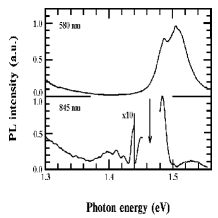
As it is clearly seen from Fig. 2 where the spectra for the


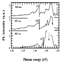
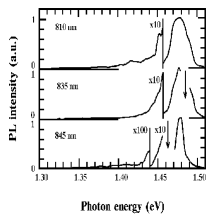
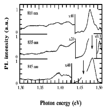
as-grown GaAs sample are presented under the interband (580 nm) and band-tail (845 nm) excitations, only the excitonic and band-edge luminescence is observed under the interband excitation, while under the bulk excitation the spectrum is much more informative. The interband excited spectra of all the samples investigated are practically identical, whereas the influence of the sample treatment is clearly seen under the band-tail excitation (Figs. 2–4). Three groups of bands are observed in the spectra of the band-tail excited PL: excitonic and hot PL ( eV), band edge luminescence ( eV), and deep centers related luminescence ( eV). The relative intensities and spectral positions of the PL bands depend on the excitation wavelength as well as the wafer treatment. Excitonic-related and hot photoluminescence depends weakly on the excitation wavelength, that reflects its surface nature, but this PL is very sensitive to the sample treatment.
This is a basic result of the current work from which a technique for correct analysis of the subsurface layer deep-level defect structure can be easily derived in application to bulk semiconductors and thick films.
The intensity of the deep-level related PL is not always a straightforward measure of the center concentration. The ratio of the extrinsic to intrinsic luminescence components is to be used to compare the center concentrations from the luminescence intensity [7]. For this reason, all the presented spectra are normalized on the band edge luminescence intensity. The excitation intensities varied from sample to sample and from one excitation wavelength to another by less than 8% during the measurements, therefore the difference between the monomolecular and bimolecular types of the deep-level and interband types of recombination is expected to be small enough. So we can use the normalized PL intensities from the spectra of different samples to compare the defect concentrations in the samples.
Not only the intensities of the corresponding luminescence bands but also the PL-bands wavelengths reflect the changes of the composition and/or concentration of the defects in the bulk and in the near-surface region because of the formation of different complexes and defect associations in the bulk as well as close to the surface that leads to the shift and/or splitting of the PL bands. Annealing or etching of the wafers can result in the changes of the intensities and the spectral positions of the PL bands because the treatments change the concentrations and compositions of defects as well as the defect associations.
3 Example of defect structure characterization: defect redistribution as a result of vapor phase epitaxy and simulating annealing of GaAs
After the treatments, dramatic changes of the PL intensities were observed. Relative intensity of the excitonic PL increased compared to the band-edge PL, while the deep-level related PL decreased, and the degree of this decrease depended on the treatment. The defect-related PL from the crystal bulk decreased by about 6 times after the annealing, and more than 10 times after the epitaxy (Figs. 2 – 4), i.e. during the treatments either the defect diffused to the surface, either the compensation of the sample changed which led to the radiative recombination centers became nonradiative, or the defects gathered in the precipitates, where they could not participate in the radiative recombination. The epitaxial growth resulted in the decrease of the defect-related luminescence. This decrease was stronger for PL at 845-nm excitation (about 100 times) and weaker for that at 810-nm excitation (about 10 times). The 810-nm excited PL from the annealed wafer and the epitaxy subjected one had comparable intensities for the bands at 1.39 and 1.41 eV, while the concentration of more deep centres close to the surface was much lower after the epitaxy than after the annealing.
Deep centers related PL had a strong dependence on the excitation wavelength that reflected the nonuniform distribution of the defects between the bulk and the near-surface layer rather than the resonance excitation of the luminescence, since all the excitation wavelengths were far from the locations of direct deep-level-to-band transitions and this PL was excited via the interband or band-tail absorption. When the excitation changed from “surface” one to “bulk” one, the increase of the deep centres related luminescence intensity with respect to the band-edge PL intensity could be clearly seen for all the investigated samples (Figs. 2 – 4).
4 Summary
Photoluminescence at band-tail excitation is a fruitful way to obtain a true
information on a real subsurface deep-level defect structure of
bulk semiconductors and thick layers. It enables the investigation
of the defect distribution deep inside the crystal bulk as well as the
redistribution of defects in subsurface layers resulting from
sample treatments.
References
- [1] Scholz R, Stahl A, Zhou X-Q, Leo K and Kurz H 1992 IEEE J. Quantum Electron. 28 2473–85
- [2] Nintunze N and Osman M A 1994 Proc. SPIE vol 2142 Ultrafast Phenomena in Semiconductors ed D K Ferry and H M van Driel pp 286–97
-
[3]
Kalinuhkin V P, Yuryev V A and Astafiev O V 1995
Mater. Sci. Technol. 11 in press
Astafiev O V, Kalinushkin V P, Yuryev V A et al 1995 Proc. 1995 MRS Spring Meeting vol 378 Defect- and Impurity-Engineered Semiconductors and Devices ed S Ashok, J Chevallier et al (Pittsburgh: MRS) in press - [4] Baude P F, Tamagawa T and Polla D L 1990 Appl. Phys. Lett. 57 2579–81
- [5] Zayats A V, Repeyev Yu A, Nikogosyan D N and Vinogradov E A 1992 Journ. Luminesc. 52 335–43
- [6] Yuryev V A and Kalinushkin V P 1995 Mater. Sci. Eng. B 33 103–14
-
[7]
Bryskevich T, Bugajski M, Lagowski J and Gatos H C 1987
J. Cryst. Growth 85 136–41
Dean P J 1982 Progress in Crystal Growth and Characterization vol 5 ed B Pampin (Oxford: Pergamon) p 89