Density-functional investigation of rhombohedral stacks of graphene: topological surface states, nonlinear dielectric response, and bulk limit
Abstract
A comprehensive density-functional theory (DFT)-based investigation of rhombohedral (ABC)-type graphene stacks with finite and infinite layer numbers and zero or finite static electric fields applied perpendicular to the surface is presented. Electronic band structures and field-induced charge densities are critically compared with related literature data including tight-binding and DFT approaches as well as with own results on (AB) stacks. It is found, that the undoped AB-bilayer has a tiny Fermi line consisting of one electron pocket around the K-point and one hole pocket on the line K-. In contrast to (AB) stacks, the breaking of translational symmetry by the surface of finite (ABC) stacks produces a gap in the bulk-like states for slabs up to a yet unknown critical thickness , while ideal (ABC) bulk (-graphite) is a semi-metal. Unlike in (AB) stacks, the ground state of (ABC) stacks is shown to be topologically non-trivial in the absence of external electric field. Consequently, surface states crossing the Fermi level must unavoidably exist in the case of (ABC)-type stacking, which is not the case in (AB)-type stacks. These surface states in conjunction with the mentioned gap in the bulk-like states have two major implications. First, electronic transport parallel to the slab is confined to a surface region up to the critical layer number . Related implications are expected for stacking domain walls and grain boundaries. Second, the electronic properties of (ABC) stacks are highly tunable by an external electric field. In particular, the dielectric response is found to be strongly nonlinear and can e.g. be used to discriminate slabs with different layer numbers. Thus, (ABC) stacks rather than (AB) stacks with more than two layers should be of potential interest for applications relying on the tunability by an electric field.
pacs:
73.22.Pr, 73.20.At, 81.05.U-I Introduction
Recently, much attention has been attracted by the class of two-dimensional (2D) graphene systems, which consist of one or a few layers of carbon atoms Novoselov et al. (2004); Castro Neto et al. (2009). Their unusual properties provided the impetus to suggest many potential applications as electronic materials Oostinga et al. (2008); Karpan et al. (2007); Nomura and MacDonald (2006). One of the key properties of graphene devices is that their electric conduction can conveniently be switched on and off. This aim has been achieved in several ways, including breaking the symmetry of a graphene sheet by depositing it on a substrate Zhou et al. (2007); Giovannetti et al. (2007), controlling its band structure by doping Ohta et al. (2006), and adjusting the electronic properties of a graphene bilayer by applying an external electric field perpendicular to the surface Oostinga et al. (2008); McCann (2006); Castro et al. (2007); Min et al. (2007). Among these methods, the latter is most promising since the electric field can easily be manipulated and the process is reversible. It has been proven that the gap of a graphene bilayer can be tuned continuously from zero to mid-infrared energies by changing the strength of the field Castro et al. (2007); Min et al. (2007).
Besides the electric field, also the stacking sequence of graphene layers influences the electronic structure of this material Latil and Henrard (2006); Aoki and Amawashi (2007); Min and MacDonald (2008); Guinea et al. (2006); Koshino (2010). Two stacking types, (AB) or Bernal stacking with hexagonal symmetry and (ABC) stacking with rhombohedral symmetry, exist besides a disordered fraction both in natural and in synthesized graphite Lipson and Stokes (1942). Here and in the following we denote the general stacking types with (AB) and (ABC), and specific stacks with AB (bilayer), ABA or ABC (trilayer), etc.
Recent work using the tight-binding approach was carried out to investigate the effect of the thickness of (AB)-type films including single-layer graphene on their -band overlap Partoens and Peeters (2006) and to study the effect of an external electric field on few-layer (AB)-graphene Lu et al. (2006). Koshino Koshino (2010) compared the tight-binding electronic structures of (AB) and (ABC) stacks in electric field and found that a gap is opened in (ABC) stacks while (AB) stacks with more than two layers stay semimetallic in the field.
Band structures of both (AB)- and (ABC)-type few-layer systems obtained by density-functional theory (DFT) calculations were examined by Latil and Henrard Latil and Henrard (2006) (without external electric field) and by Aoki and Amawashi Aoki and Amawashi (2007) (with external electric field). The electric-field response of the DFT band structure of an ABC-trilayer was investigated by Zhang et al. Zhang et al. (2010). On the experimental side, the existence of ABAB and ABCA stackings in tetralayer graphene was recently proved by infrared absorption spectroscopy in combination with tight-binding calculations; no other tetralayer stackings were found Mak et al. (2010).
For bulk systems, on the other hand, clear evidence that rhombohedral graphite is a true carbon allotrope seems to be lacking, see Ref. Cousins, 2003 and references therein. The available data point to the occurrence of about ten-layers thick (ABC) stackings with areas in the order of unit rhombi in filings from single crystals Cousins (2003). A comparative DFT study of (A), (AB) and (ABC) bulk systems was performed by Charlier et al. Charlier et al. (1994). Obviously, Bernal-type graphite (-graphite) is energetically more stable than rhombohedral graphite (-graphite) Charlier et al. (1994); Cousins (2003) and has been studied much more intensely than the latter.
The most important structural difference between (AB)- and (ABC)-type stackings is that the (AB) stacking shows straight lines of bonds connecting all atoms of one sub-lattice perpendicular to the layers through the whole stack, whereas in the (ABC) stacking only single pairs of atoms are connected perpendicular to the layers, see Fig. 1. In other words, in (AB) stacks there are two kinds of atoms, one with dangling bonds in both -directions and the other without any dangling bonds, whereas in (ABC) stacks each atom has one dangling bond, either in positive or in negative z-direction. Evidently, this difference must have a large impact on the structure of the -bands.
The present paper is devoted to a comprehensive study of the electronic structure and the dielectric response of stacks of graphene by means of high-precision DFT calculations combined with a topological analysis at tight-binding level. While the focus lies on the hitherto less intensely studied rhombohedral stacks including bulk -graphite, comparison with AB-bilayers and other Bernal stacks is made in appropriate places below.
Computational details with emphasis on the correct treatment of external electric fields applied to 2D slabs are outlined in Section II. Section III A contains a critical comparison of the AB-bilayer band gap versus external electric field with related literature data and the low-energy band structure of few-layer (ABC) systems with and without field. The low-energy states are characterized as surface states in Section III B. Further, we provide evidence that (ABC) slabs have a gap in their bulk-like states only up to a critical thickness. A detailed band structure of bulk -graphite is shown and discussed in critical comparison with literature data. In Section III C, we discuss the topological distinction between rhombohedral stacks and Bernal stacks. The former are shown to possess topologically protected zero-energy surface states. Next, the field-induced charge densities of bi- and 6-layer systems and an analysis of induced dipole moments for single- and bilayer systems are provided in Section III D. The analysis of the electric field response is continued in Section III E by comparing the field-induced charge transfer with the chemical charge transfer, in Section III F where conclusions for the modelling of the dielectric response of graphene stacks are drawn, and in Section III G where local densities of states without and with external field are shown. The field-dependent dielectric constant of few-layer stacks is presented in Section III H. Finally, the main results are summarized and conclusions are drawn in Section IV. Earlier arguments by Aoki and Amawashi Aoki and Amawashi (2007) concerning a better electric tunability of (ABC) stacks compared with (AB) stacks are confirmed and extended.

II Computational details
DFT calculations have proven to be powerful in predicting the ground state properties of various systems, including three-dimensional (3D) bulk and 2D thin films without and with external electric field. In this context, 2D films are frequently modeled by forming a 3D system from periodically stacked slabs with vacuum regions in between. There is however one severe problem with a straight application of the supercell approach for 2D slabs in self-consistent calculations with external fields. The field-induced dipole moment of a single slab causes a potential difference between the vacuum regions on the two sides of the slab. This induced potential difference would break the translational invariance of the supercell. It is, thus, compensated by a linear potential term forced by the periodic boundary conditions in a straight application. This linear term is not harmful in the vacuum region but it reduces the induced (screening) potential inside the slab and thus enhances the effective external field to a degree depending on the ratio between vacuum and slab thickness.
In order to avoid these problems, Kunc and Resta Kunc and Resta (1983) applied a sawtooth-like external potential with symmetric teeth of alternately rising and descending flanks. This potential can be implemented by introducing alternately positive and negative capacitor plates into the vacuum regions. In this model, two neighboring slabs form a double cell, where the dipole moments of both slabs cancel each other and the periodicity of the potential is saved. To circumvent the extra numerical effort by doubling the supercell, Neugebauer and Scheffler Neugebauer and Scheffler (1992) (see also a similar approach in Ref. Bengtsson, 1999) proposed to use an asymmetric external sawtooth potential with ascending flanks followed by jumps. They introduced artificial dipole layers in the vacuum region to compensate the induced dipole moments. Although both methods produce a periodic potential, which provides in principle the same electronic structure within the periodic slabs as within a single slab, there are inaccuracies if the vacuum region is not wide enough, and the extra discontinuities in the effective potentials worsen the convergence of Fourier transformation-based 3D methods.
Within the FPLO (full-potential local-orbital) approach fpl , Tasnádi recently implemented a single-slab method which guarantees the correct boundary behavior in the vacuum region F.Tasnádi (2007). Like in similar isolated-slab methods FLE , the advantages of this approach are the following: (1) there are no side effects of any artificial periodicity, (2) the external electric field is smooth everywhere, and (3) the electrostatic properties can be calculated correctly without any dipole correction.
Most of the presented results, in particular the data of Table 1 and of all figures except Figs. 4, 5, 6, 8, 9, and 11 were obtained with the FPLO-slab-1.00-10 code F.Tasnádi (2007). The data of the other figures, where no external electric field is considered, were calculated with the FPLO-code fpl ; Koepernik and Eschrig (1999), version , in a 3D supercell approach. The local density approximation (LDA) with the exchange-correlation (XC) parameterization by Perdew and Wang Perdew and Wang (1992) was applied in all calculations.
Fixed geometries according to Fig. 1 with Å C-C bond length and Å not (a) inter–layer distance were used both in the 2D and 3D approaches. Thus, possible surface relaxations and bucklings were disregarded. On the other hand and at variance with tight-binding model calculations, surface effects on the charge distribution and influence of the stacking and the surface on the hopping parameters are taken into account in a self-consistent manner. Further, since the present investigation is focussed on the electronic structure and not on structural or elastic properties, the fixed inter–layer distance avoids any functional-dependence of the geometry which might be relatively large for weak bonds. In the supercell calculations, a well-converged vacuum thickness of 16 Å was chosen. The following space groups were taken: 166 for bulk -graphite, 143 for 3D supercells, and 69 (layer group p3m1) for 2D slabs.
The basis set comprised carbon 1, 2, 2, 3, 3, and 3 orbitals. It was enhanced by including orbitals for the calculation reported in Fig. 11 in order to obtain a precise empty-states band structure.
If not stated otherwise, we used a k-mesh of points in the full Brillouin zone (FBZ) for the slab calculations and of points for the supercell calculations in a linear tetrahedron method with Blöchl corrections.
In order to cross-check the FPLO results and to elucidate the role of the dipole correction in 3D supercell calculations, we compared AB-bilayer results of the pseudo-potential code QUANTUM-ESPRESSO-3.2.3 (QE) in supercell geometry esp ; Giannozzi et al. (2009) (both with and without dipole correction, Fig. 2) with the FPLO slab results. The same atomic positions and LDA version were used in QE and FPLO calculations. In QE, a supercell height of Å (implying a vacuum thickness of Å) was used. An external sawtooth-like potential was applied with linear increase between Å and Å (slab centered at ) and linear decrease in the remaining region. The cut-offs used in QE are 40 Ryd for the wave functions and 480 Ryd for the charge density. We obtained converged band gaps with a k-mesh of points and a cold smearing of 0.0001 Ryd (Monkhorst-Pack sampling).
III Results and discussion
III.1 Field-dependent band structure of AB, ABC, ABCA, and ABCAB stacks
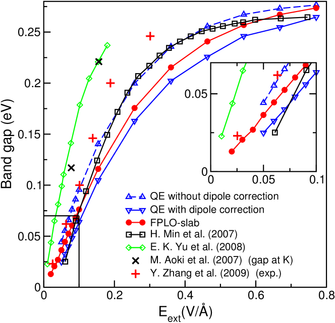
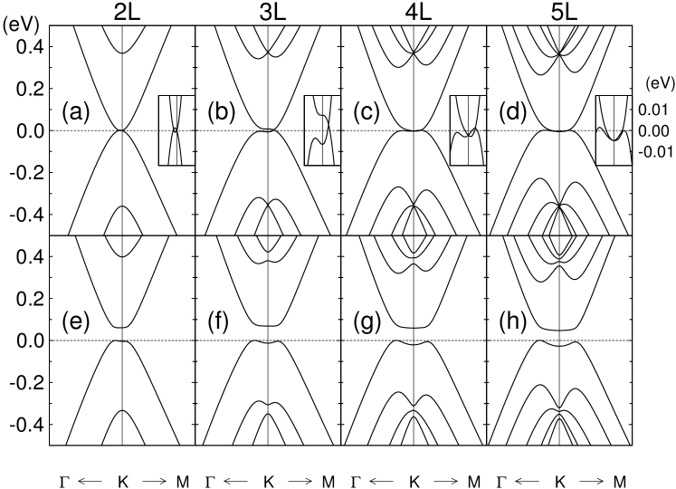
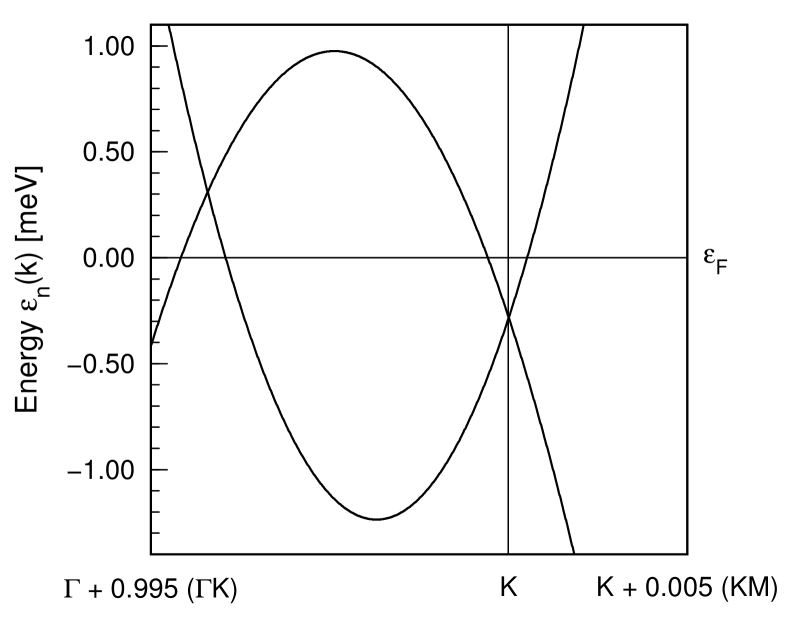
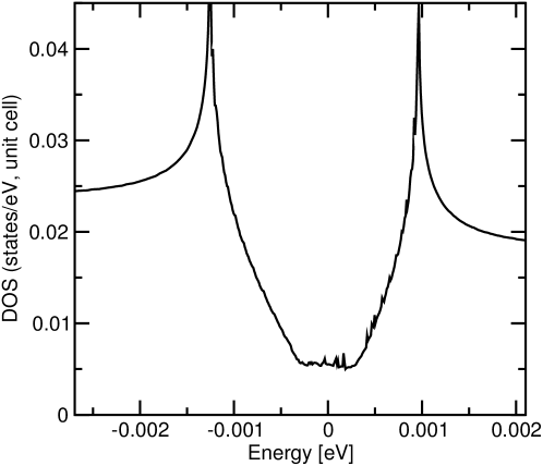
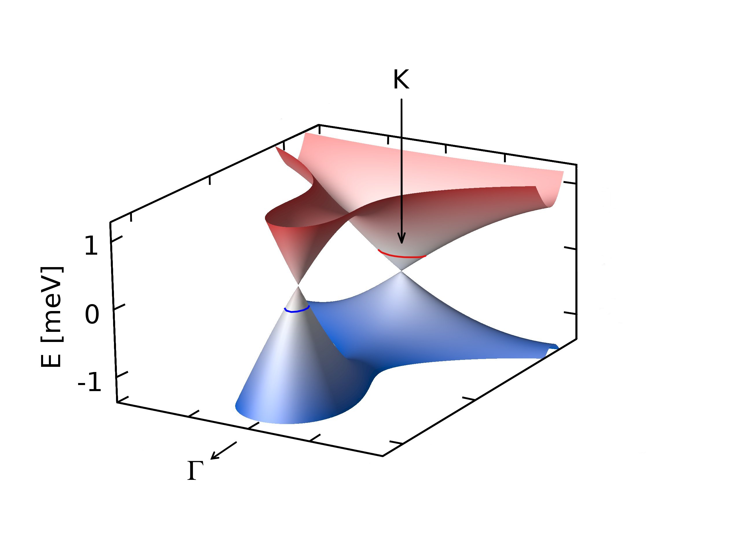
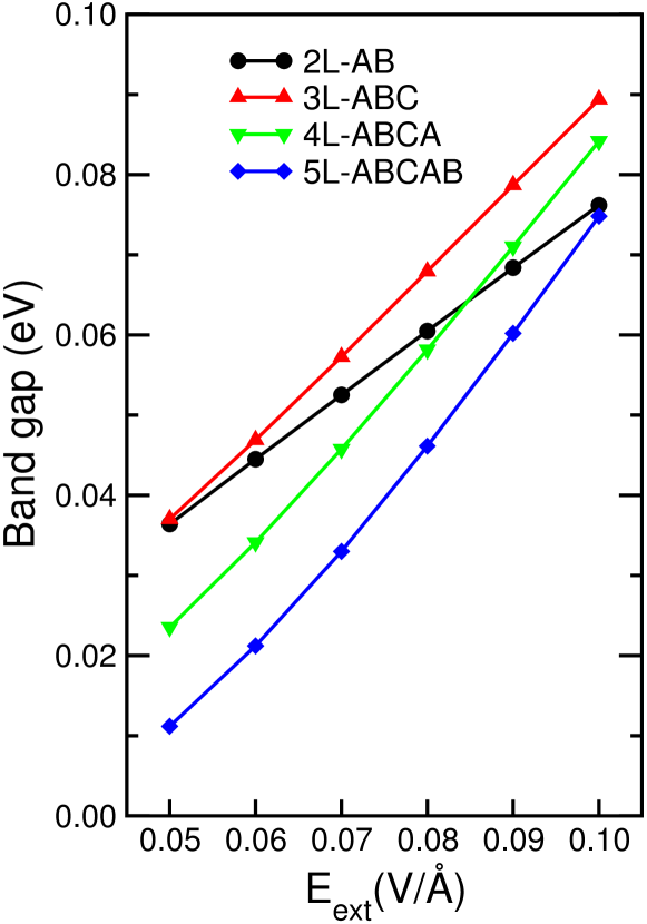
Fig. 2 shows calculated band gaps of graphene AB-bilayers in an external electric field using different approaches and codes. We first note, that the dipole correction in QE decreases the band gap substantially. According to our discussion in the previous section, the induced screening field inside the slab is artificially reduced by approximately a factor (vacuum thickness divided by supercell height), if the dipole correction is omitted, thus enhancing the effect of the external field. For the given choice of QE parameters and V/Å, the band gaps obtained using QE with and without dipole correction amount to 64 meV and 96 meV, respectively. The band gaps calculated with the FPLO-slab code, which does not need a dipole correction, are about 1015 meV larger than those obtained with the QE-code with dipole correction. All FPLO data fall in between the QE data with and without correction, thus providing confidence in the new slab approach. Notably, our and most of the other values are smaller than the experimental values deduced from infrared absorption Zhang et al. (2009). This can be attributed to the fact that DFT (even if it could be done exactly) systematically underestimates the Kohn-Sham gap width Hybertsen and Louie (1986).
The energy distance between the two Dirac points of the semi-metallic AB-bilayer is very small, 0.8 meV Latil and Henrard (2006) or even less (see our results below). Thus, a small but finite external electric field is needed to open a gap in this system. Indeed, an extrapolation of the experimental data in Fig. 2 yields a field of about 0.003 V/Å necessary to open a gap. This value coincides with the extrapolated FPLO-slab result. On the other hand, extrapolation of the data by Min et al. Min et al. (2007) provides a critical field about one order of magnitude larger, while the data by Yu et al. Yu et al. (2008) point to a small gap even at zero field (see insert in Fig. 2). In order to suggest possible reasons for the severe deviations between our results and the other published DFT data, we note the following problems. In the calculation by Min et al. Min et al. (2007), a single bilayer was placed in a supercell without applying a dipole correction. This could explain the similarity between their data and the uncorrected QE data for intermediate fields. Further, these authors used a relatively fine k-mesh of 5,000 points in the 3D FBZ, which however might still be too coarse at lower fields. Note, that our calculations were carried out with an ultra-fine mesh of 90,000 points in the 2D (sic) FBZ. Yu et al. Yu et al. (2008) employed a perturbative bulk approach based on the modern Berry-phase technique to investigate the effect of a homogeneous electric field. To the best of our knowledge, this approach is also lacking the dipole correction for the study of slabs. Moreover, this method yields for the (semi-)metallic case of bulk -graphite an unphysical finite bulk polarization Yu et al. (2008) which might point to problems of the method with small- and zero-gap systems. These authors applied a -sampling with 900 points in the 2D FBZ. Finally, also Aoki and Amawashi Aoki and Amawashi (2007) do not mention dipole corrections and used a k-mesh with 100 points in the 2D FBZ.
Fig. 3 shows band structures near the K point for 25 layers of graphene with stackings AB, ABC, ABCA, ABCAB. The first and the second row display the electronic structure without and with external electric field, respectively. The inserts in the upper row show some subtleties at the meV scale with ten times magnified energy scale. Corresponding figures for the (AB) stacked systems can be found in Ref. Lu et al., 2006 (tight-binding approach with overlap integrals from bulk graphite) and in Ref. Latil and Henrard, 2006 (self-consistent DFT-calculations with the ABINIT code).
Apart from details on the meV scale, visible in the magnifications in Fig. 3, the results from a self-consistently screened minimum-basis tight-binding Hamiltonian taking into account only the interaction parameters and from bulk graphite (see Fig. 4 in Ref. Koshino, 2010) agree qualitatively with Fig. 3. Such a qualitative agreement holds even in the meV-range, comparing our self-consistent DFT results for zero electric field (inserts of Fig. 3) with Fig. 5 of Ref. Koshino and McCann, 2009, where the low-energy band-structure of rhombohedral stacks was obtained in a tight-binding approximation taking into account the interaction parameters . On the other hand, we note large quantitative differences between the DFT results and self-consistently screened tight-binding data. For example, the AB-bilayer band gap, Fig. 2, is a factor of about two smaller than the related band gap shown in Fig. 6 of Ref. Koshino, 2010. A possible reason for these differences will be discussed in Section III F.
Before we further discuss the results for stacks with 3, 4, and 5 layers, we have a look at the bilayer results with yet higher resolution, Figs. 4, 5, and 6. The band structure in Fig. 4 agrees qualitatively with the DFT result published in Fig. 4a of Ref. Latil and Henrard, 2006 where the ABINIT code was used. Our energy difference between the local extrema – called in Ref. Latil and Henrard, 2006 – is 2.2 meV compared with 2.6 meV in Ref. Latil and Henrard, 2006. Also, the energy difference between the Dirac points amounts to 0.6 meV (Fig. 4) vs. 0.8 meV (Ref. Latil and Henrard, 2006). An important difference is, however, that in Ref. Latil and Henrard, 2006 the intersection of both bands (the “Dirac point”) at the K-point coincides with the Fermi energy, leaving only a hole pocket on the line -K. This is not correct because the volume of the electron- and hole-pockets must be equal in neutral carbon stacks. In order to get an accurate Fermi energy we chose the -grid in such a way that at both intersection points of the two bands mesh points for the linear tetrahedron method are located. Then the linearly interpolated bands, which are used for the calculation of the density of states, reproduce the real band structure around the band intersections as good as possible. To be specific, a mesh with points in the 2D FBZ was used to obtain the accurate position of the Fermi level in Fig. 4. In order to achieve reasonable resolution in Fig. 5, a special mesh of points was employed. This mesh was chosen such that it fills only about 0.1% of the 2D FBZ around the K-point, the only region where states in the energy window of interest are present.
The simplest two-parameter tight-binding model for the bilayer (considering only and ) provides a semi-metal with two touching parabolas at the K-point McCann and Fal’ko (2006); Guinea et al. (2006), leaving no Fermi surface at all. If additionally is taken into account, the bands show the two “Dirac cones”, but both have the same energy (namely the Fermi energy) and there is no Fermi surface without doping McCann and Fal’ko (2006). Our result, Fig. 4, means that the prediction of a Lifshitz transition to a gap-less state Lemonik et al. (2010), which rests on a band structure model including only these 3 overlap integrals, has to be revisited. On the other hand, the numerical tight-binding approach in Ref. Lu et al., 2006 which considered the 7 most important overlap integrals from bulk graphite shows an energy difference in the two cusps, but in the opposite order compared with the self-consistent DFT approaches (i.e. the crossing at point K is higher in energy than the other one). In other words, Ref. Lu et al., 2006 provides a hole pocket around K unlike the electron pocket in our self-consistent DFT approach. Consequently we have to state, that the meV-features and the topology of the Fermi surfaces are very delicate and tight-binding results using overlap parameters from bulk graphite may not agree with the results from self-consistent DFT calculations. A similar conclusion was drawn for the ABC trilayer case in Ref. Zhang et al., 2010.
Fig. 6 shows the band structure of an AB-bilayer close to the Fermi level in a 3D representation. The hole pocket on the -K line is nearly elliptical (with the axis along -K being 3 times longer than perpendicular to it) and the electron pocket around K is roughly a circle with a slight deformation maintaining a three-fold symmetry according to the symmetry of the band structure at the K point. An estimate using a model with linear dispersion and circular (electron pocket around K) and elliptical (hole pocket on -K) iso-energy curves provides for the number of holes (which equals the number of electrons) in the pockets the tiny value of per unit cell, or equivalently, per atom. The density of states (DOS) at the Fermi level obtained from the same model is for both holes and electrons (which need not to be equal) approximately states per eV per unit cell. This agrees well with the numerical value seen in Fig. 5. The peaks in the DOS of Fig. 5 are actually logarithmic singularities resulting from the saddle points between the two Dirac points (see Fig. 6). The two kinks at the bottom of the valley between the peaks are located at the Dirac point energies.
We now resume the discussion of stacks with more than two layers, Fig. 3. Without external field, the ABC stack is a zero-gap semi-conductor, while the ABCA and ABCAB stacks show a small overlap between the valence and the conduction band near the K point. This confirms previous DFT results on ABC stacks Latil and Henrard (2006); Zhang et al. (2010) and on ABCA stacks Latil and Henrard (2006). These findings together with the information that also (i) all other rhombohedral stacks with up to ten layers and bulk -graphite (see Section III B) are found to be semi-metallic in our DFT calculations and (ii) stacks with layers were found to be semi-metallic in a tight-binding approach with five hopping parameters Koshino and McCann (2009) leads us to claim that except the trilayer all rhombohedral stackings are semi-metallic.
As a general feature, we notice in Fig. 3 that for an arbitrary number of layers , there are only two bands near the Fermi level, and bands around eV. These two bands at the Fermi level were identified in earlier tight-binding calculations as surface states Guinea et al. (2006); Min and MacDonald (2008). When an external electric field is applied, the conduction band becomes flat and the valence band becomes a little concave at the K point. Further, the degeneracy around eV is lifted.
Fig. 7 shows the calculated minimum gap for the AB-bilayer and for graphene layers with (ABC)-type stacking as a function of the external electric field ranging from to V/Å. Due to the subtleties in the band structure around the Fermi energy, our self–consistent procedure did not converge for the 35 layer systems in small (but non–vanishing) external fields below approximately V/Å. Our results show that all considered systems have a band gap in the considered fields, though they are semi-metallic at zero field. In all cases the band gap increases with in the considered range.
The prediction that a gap is opened for (ABC) stacks by an external electric field differs from the behavior reported for systems with Bernal stacking and . There, diverse results were obtained by tight-binding calculations. While Lu et al. found that small gaps for ABA- and ABAB-slabs exist in finite external field ranges (see Fig. 4 of Ref. Lu et al., 2006), Koshino Koshino (2010) reported that these systems and also (AB) stacks with more layers stay semimetallic in a moderate field. DFT calculations for ABA- and ABAB-slabs support the latter result Aoki and Amawashi (2007).
For the AB-bilayer the general trend in the gap width with external field has been experimentally verified Zhang et al. (2009). Also, field-induced band gaps were obtained for (ABC) tri- and tetralayers by means of earlier DFT calculations Aoki and Amawashi (2007); Zhang et al. (2010).
Extrapolation of the band-gap vs. field curves of Fig. 7 to zero field should yield a zero band gap for the trilayer and a very small negative band gap of about meV for the other systems, corresponding to the band overlaps visible in Figs. 3 and 4. While this can be achieved by an almost linear extrapolation for the bilayer system, non-linear behavior is expected from our data for all other systems. Thus, we predict a positive curvature of the low-field band-gap vs. field dependence for rhombohedral stacks with three and more layers, where the non-linearity increases with the number of layers.
III.2 Bulk limit and surface states
An intriguing trait of the electronic structure of finite (ABC) stacks is that all states in the vicinity of the Fermi energy are localized near the two surfaces. This was recently demonstrated for stacks of arbitrary thickness by tight-binding model calculations Koshino and McCann (2009). Here we show by DFT calculations, that there must be a finite thickness beyond which the bulk gap is closed and the whole slab turns semi-metallic.
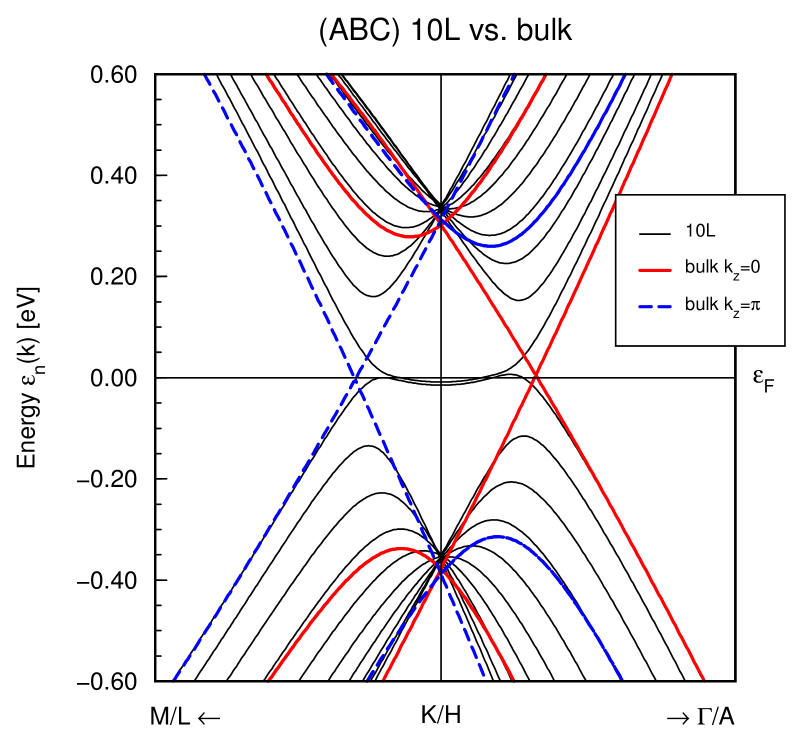
We first discuss the DFT results for slabs of finite thickness and for bulk rhombohedral graphite. In addition to the results on up to five layers, Fig. 3, consider the 10-layer result (for ) shown in Fig. 8. We observe in all stacks a pair of bands at the Fermi level which is very flat over an increasing part of the k-space around the point K, if the number of layers is increased. The detailed behavior is complicated for thinner slabs with as seen in Fig. 3 and also for , not shown. For it however resembles qualitatively the behavior seen in Fig. 8 showing two nearly parallel lines over a large k-space region. The Fermi energy lies amidst these two almost parallel bands. This behavior is a refinement of the dispersion provided by the simplified model in Ref. Min and MacDonald, 2008. Tight-binding calculations taking into account the interaction parameters show the same behavior for . Unlike our results, these calculations still show crossings of the two bands for , Fig. 5 of Ref. Koshino and McCann, 2009, but the band overlap is considerably smaller than for lower .
A crucial point is that the wave functions belonging to the states
of close proximity to the Fermi energy are strongly localized at the
slab surfaces, whereby each band is localized on one surface.
At the K symmetry point, 99% of the related band weight belongs
to the top or surface layer.
If we follow these two bands away from the K point to the
regions where the splitting becomes increasingly larger,
they gradually turn into bulk-like states.
The weights of all other bands,
which do not intersect the Fermi level, are spread all over the slab,
i.e., they are bulk-like.
This interpretation is supported by consideration of the
projected bulk band structure (PBBS,
projected onto the plane parallel to the slab)
shown in Fig. 9.
The PBBS rests on periodic boundary conditions in all 3 dimensions.
Concerning the relation between the PBBS
and slab band structures for ,
the following theorems are familiar from surface band theory:
(i) The modulus of all slab states turns asymptotically
(in inward direction) either into
periodic bulk states or into surface states
with an exponentially decaying envelope.
(ii) The energy of the bulk states agrees exactly with the
corresponding states in the PBBS.
Therefore, all bulk bands lie within the continuum of the PBBS.
(iii) For given , the component of the Bloch vector parallel
to the slab, all states in gaps of the PBBS are surface states.
Fig. 9 shows that the boundaries of the PBBS
in the central rhombic gap region are identical with the Dirac-like bands
for and , also shown in Fig. 8.
There, we can focus our attention to the space around the line K-H,
because in all other regions the bulk bands are far away from the Fermi level.
It follows from the above mentioned theorems,
that the pair of states in the central rhombus of Fig. 8
have to be surface states, provided, this pair stays there in the limit
.
This conclusion coincides with the mentioned investigation of the
weights of the Bloch states.
Our discussion also explains, why the pair of surface bands
turns into bulk bands upon immersion into the PBBS.
The bulk-like states of the 10-layer slab in Fig. 8 are not yet completely localized within the boundaries of the PBBS. However, we checked that with increasing the energies of the bulk-like states at K move closer to the Fermi energy making a complete overlap for very likely.
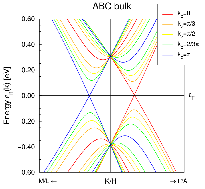
It follows from Fig. 9, that the low-energy band structure of bulk -graphite consists of four bands with linear (Dirac-like) dispersion. Two of these bands cross the Fermi level close to the K-point, the other two close to the H-point. This crossing is not lifted by spin-orbit interaction. The “Dirac points” on the planes and have an energy difference of 9 meV and lie above and below the Fermi energy, respectively, giving rise to tiny hole and electron pockets in the bulk band structure. Thus, bulk -graphite is a semi-metal. From the fact that the Dirac points for are found slightly below and slightly above the Fermi level we conclude, that the gap of the bulk-like states already closes at a large but finite stack thickness, .
a)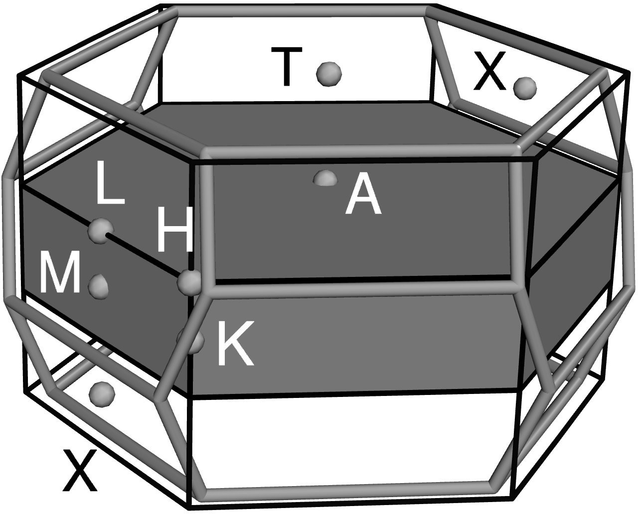 b)
b)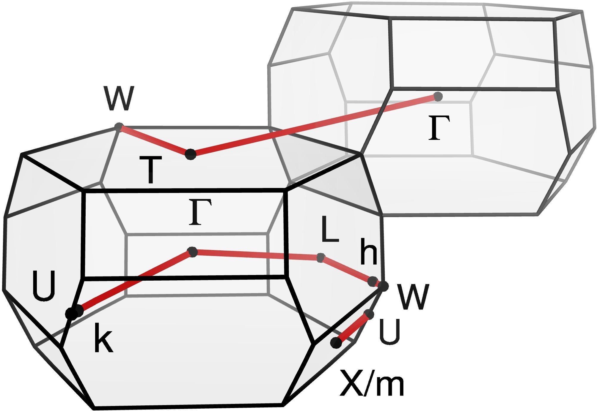
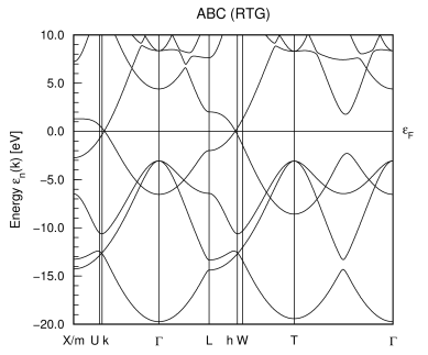

We close this subsection by showing the band structure of bulk -graphite in a more complete overview. This aims at clarifying the position of the two Fermi-level Dirac cones in the rhombohedral trigonal (RTG) BZ and at comparing with previously published band structures Charlier et al. (1994). In Fig. 10a the relation between the RTG (2-atom setup) and the hexagonal (6-atom setup) BZs is shown. The first BZ of the hexagonal setup is drawn opaque in the center of the rhombohedral BZ. The hexagonal high symmetry points are labelled in white, the RTG points T and X in black. The first hexagonal BZ can be shifted by a reciprocal lattice vector of the hexagonal lattice, which gives the two transparent cells above and below the opaque cell in the figure (shift by ). Note, that the X-point (the T-point) of the RTG BZ coincides with the M-points (the A-points) of the shifted hexagonal cells. This leads to a back-folding of the bands around the X-point (T-point) onto the M-point (A-point), when the hexagonal 6-atom setup is used. In Fig. 11 (lower panel) the bands obtained from an RTG 2-atom setup along the three paths -M-K--A-L-H-A of the three hexagonal cells are plotted into one figure. The resulting band structure is equivalent to the one obtained from a straight-forward 6-atom hexagonal setup.
Comparing the band structure of Fig. 11 (lower panel) with Fig. 3 of Ref. Charlier et al., 1994 we find that both band structures agree except on the symmetry points K and H and the related symmetry lines. It was already noted by the authors of Ref. Charlier et al., 1994 that the wide-gap insulating behavior found in their hexagonal setup is not correct. Instead, they find a band crossing close to the Fermi level on the line L-W in the RTG setup and an avoided crossing on -X.
In Fig. 11 (upper panel) the band structure as obtained from the RTG setup along the path shown in Fig. 10b is shown. Note, that the part X/m-(U)-k- and the part L-h-(W)-T correspond to the parts M-K- and L-H-A of Fig. 11 (lower panel), respectively. Of course, only the bands belonging to the centered hexagonal BZ (opaque in Fig. 10a) are present. The RTG band structure shown in Fig. 11 (upper panel) agrees qualitatively with that published in Ref. Charlier et al., 1994, Fig. 4, with the severe difference that we find a crossing on -X. We conclude, that the two Dirac cones close to the Fermi level of the band structure of bulk (ABC) graphite shown in Figs. 8 and 9 originate from band crossings on two symmetry lines of the RTG BZ which coincide with symmetry lines of the hexagonal BZ.
III.3 Topological nature of the surface states
A remarkable and until now obscured characteristic of the surface states, present in finite (ABC)-stacked graphene, is their topological nature. It has been demonstrated in the literature Guinea et al. (2006) that a low energy, long wavelength model (expanded around the K-points of the basal 2D Brillouin zone) for stacked graphene layers can be mapped onto a formally equivalent one-dimensional (1D) problem, reminiscent of electrons moving along a 1D chain. One can define such a mapping for Bernal-stacked graphene as well as for rhombohedral stacking, resulting in two distinct effective 1D chain models. When considering two hopping processes Guinea et al. (2006), the tight-binding model for electrons moving along a 1D chain derived from rhombohedral stacking is in turn equivalent to the famous Su-Schrieffer-Heeger model for a dimerized chain Su et al. (1979); Jackiw and Rebbi (1976). The latter model is known to accommodate both trivial and non-trivial topological phases, depending on the relative strength of the hopping parameters. The consequence of non-trivial topology is the existence of zero energy modes, localized on the edges of the 1D chain.
From this perspective, the surface states in (ABC)-stacked graphene emerge as a consequence of the non-trivial topology of the bulk model system, which is revealed by the formal mapping onto a 1D chain. In order to clarify the topological distinction between rhombohedral graphite (RG) and Bernal hexagonal graphite (BHG) in the tight-binding approximation, we briefly discuss the 1D models derived from them, taking into account in-plane nearest neighbor hopping and vertical nearest neighbor interlayer hopping . Both for BHG and RG the mapping onto a 1D chain renders a problem with a two-site unit cell. We label the two sites and and use the wave function basis , where designates the chain unit cell, . The two hopping processes in RG lead to the effective inherited hopping parameters and for the chain. Here, , denoting the in-plane carbon-carbon distance and the in-plane momentum in the basal BZ with respect to the K-point. In both cases, RG and BHG, we can transform to momentum space. In terms of the momentum along the chain, which we call to avoid confusion, the respective Hamiltonians for RG and BHG read
| (1) |
and
| (2) |
where are the Pauli-matrices (). Based on these expressions we can immediately identify how they fit into the generic form of any 1D two band Hamiltonian, given by . The topological properties are contained in the vector , which reads for RG and for BHG . The vector may be considered as a mapping from the circle (due to the periodicity in ) to the 2D plane not (b). The topological distinction between the two models can now be explicitly formulated in terms of the winding of the -vector around the origin, as is cycled from 0 to . It is easy to see that for BHG there is no possibility for winding around the origin, while for RG the -vector does wind around the origin if . The latter inequality then is the condition for non-trivial topology and hence the presence of edge states (surface states). It is in full agreement with the results reported in Ref. Guinea et al., 2006, but here derived from topological arguments. From this simplified picture we can gain qualitative insight in the projected band structure shown in Fig. 8. The surface states appear in the vicinity of the K point, for small momenta , and have zero energy. At some point the bulk bands touch after which, for larger , the surface states have disappeared.
The same kind of reasoning can be applied to models that take into account additional hopping processes. We have investigated a more involved tight-binding description of (ABC)-stacked graphene layers, including hopping processes , , and , and found analytically (for ) and numerically (for ) that the topological distinction is retained. There remains an area in the in-plane k-space where topological zero-energy modes exist. We would like to recall, however, that the DFT results of the previous subsection indicate a bulk (semi)-metallic state for slabs with . Thus, the predicted surface metallic behavior will turn into bulk metallic behavior with surface states present in the bulk gap for very thick slabs.
The interpretation of the surface states in terms of topology leads to an interesting speculation, since zero-energy modes in the 1D dimerized chain are not only expected on the edges, but also localized at domain walls separating topologically distinct phases. In RG one would expect these zero modes to appear when the stacking sequence is reversed somewhere in the bulk, going from ABCABC to CBACBA. They would be bound to the layer where the reversal occurs and may have potentially interesting properties, different from stacking faults in Bernal stacked graphene. The same kind of zero-energy modes should be present at boundaries between (ABC) and (AB) stackings.
III.4 Induced charge density and dipole moment
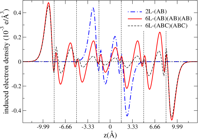
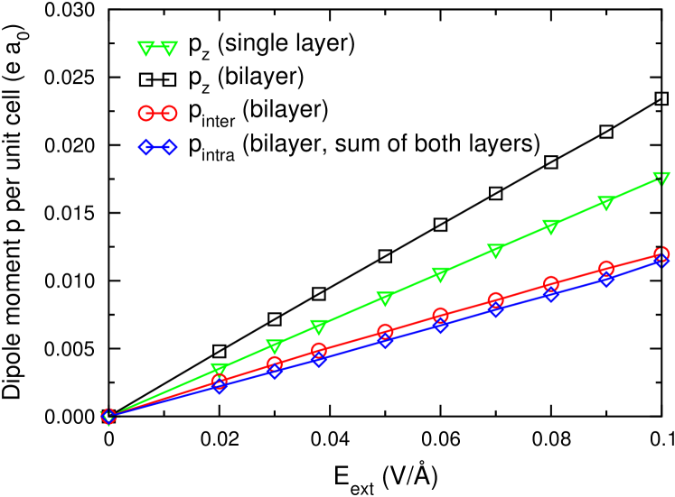
We proceed with the discussion of few-layer stacks in an external electric field along the -direction. A detailed analysis of the field-induced charge density exhibits some interesting features which are not shown by non–selfconsistent tight binding models. We consider an average of the induced charge density in the plane, , which can be used to evaluate the induced dipole moment per unit cell ,
| (3) |
where denotes the elementary charge and the area of the unit cell in the plane.
The behavior of presented in Fig. 12 shows a significant asymmetry around each carbon plane. Thus, it makes sense to distinguish an intra-layer and an inter-layer contribution to the dipole moment, . We intend to analyze these contributions only for the bilayer case and define . Here, denotes the induced charge per layer, obtained as sum of projections to the two atomic sites, and Å is the layer distance. Fig. 13 shows that in the bilayer both contributions have approximately equal size. Both contributions produce a dipole moment in the same direction which is consistent with the classical notion of a density shift in the direction of the Coulomb force due to the external field. Fig. 13 includes also the dipole moment calculated for a single layer (graphene), which is about three times larger than the intra–layer contribution of one layer in a bilayer system (observe, that the related curve in Fig. 13 shows the sum of both intra–layer contributions in the bilayer system). The reason for this difference is that in a mono-layer system there is no inter–layer charge transfer that screens an essential part of the external field.
Fig. 12 shows the planar average of the induced electron densities for an AB-bilayer and for 6-layer systems with (AB) and with (ABC) stackings. Due to the screening of the external field the amplitudes of the induced electron density are significantly smaller in the interior of the 6-layer slabs than on their surface. This feature is in contrast to the results for (AB) stacks published in Ref. Yu et al., 2008, where the amplitudes of the induced electron densities in the middle of the 6-layer system differs from the surface layer amplitudes by a few percent only. These results however refer to electric fields which are one order of magnitude weaker than in our calculation. In order to ensure reliability of our data, we repeated the FPLO calculations with the QE code and found virtually the same results. Note, that both codes are completely independent. Not understandable from a fundamental point of view are induced electron densities published in Ref. Yu et al., 2008 for bulk graphite. Though -graphite is metallic and should not show any induced charges in the bulk, the induced bulk charge densities shown in Fig. 3(d) of Ref. Yu et al., 2008 are yet larger than the surface charge densities of the 6-layer slab.
It is interesting to note, that the ABABAB slabs show a larger induced screening charge density in the inner layers than the ABCABC slabs. This seems to contradict the fact, that ABABAB slabs stay metallic for the electric field range in question, whereas the ABCABC slabs turn semi-conducting. Qualitatively, the same trend is seen in the results from the simplest possible tight binding model calculation Koshino (2010). We suggest that the observed astonishing behavior can be understood from the different character of states contributing to the screening. In rhombohedral stacks, only the two surface states are close to the Fermi level. Thus, the screening charge density is concentrated close to the surface. In Bernal stacks, states are present at the Fermi level in the absence of an external field. Hence, screening charge density is contributed from a number of layers if a field is applied. Obviously, the hand-waving argument that screening in metals is more effective than in semi-conductors does not necessarily apply to few-layer slabs, where the asymptotic exponential behavior is not yet valid. The following analysis will however show, that the layer-integrated charges decay on a shorter length-scale than the charge densities.
III.5 Inter-atomic charge transfer
chemical electron transfer
physical electron transfer
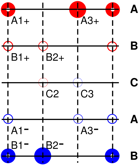
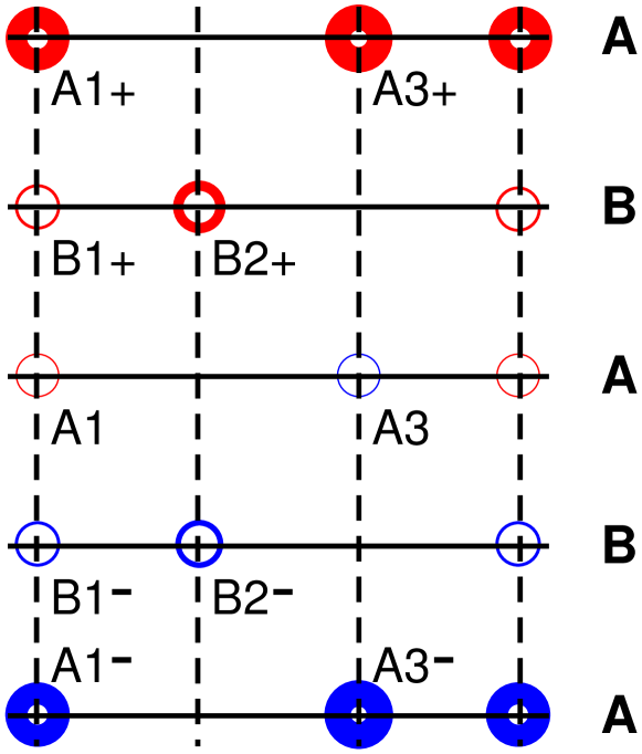
Table 1 and Fig. 14 show the electron transfer between the atoms for both (ABC) and (AB) stacking, calculated by atomic site projections.
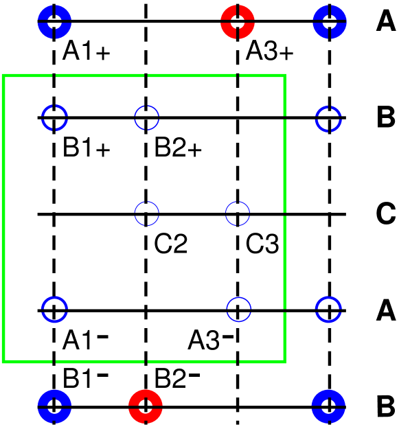
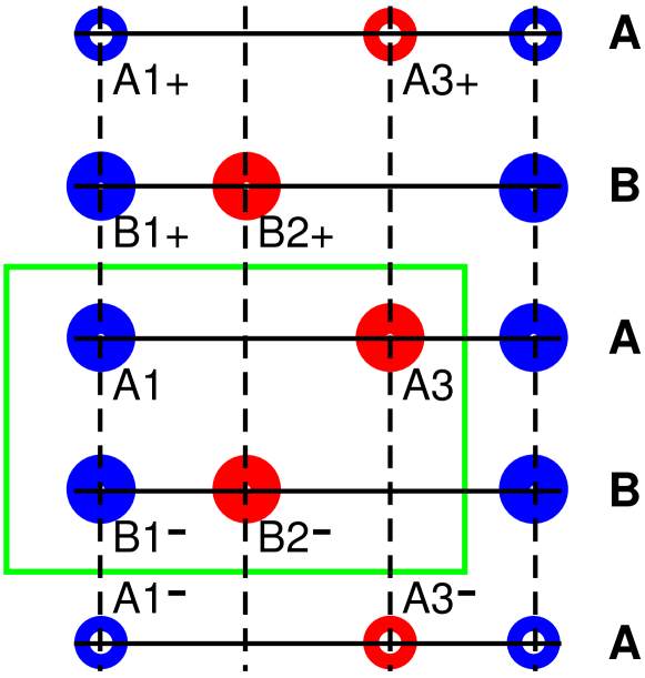
Without external field (see upper panel of Fig. 14 and left columns of Table 1) the layers are not completely neutral (except in the bilayer case), but there is a small electron transfer toward the surface so that the surface layer is slightly negatively charged. The electron flow from the interior to the surface produces a surface dipole barrier and decreases the ionization energy or work function. Additionally, there is a much stronger chemical intra-layer transfer away from saturated bonds towards dangling bonds (e.g. from position ’1’ to ’2’ or ’3’ in the surface layers in Fig. 14). For (ABC) stacking, this transfer converges to zero toward the interior, because in the bulk all six lattice positions in the repetition unit are physically equivalent for symmetry reasons. (Note that the bulk unit cell for (ABC) material is different from this repetition unit: it contains only two atoms and has rhombohedral symmetry.) For (AB) stacking, however, the intra-layer electron transfer converges to a finite value, because there are two different lattice positions in the unit cell: one has only saturated and one has only dangling bonds, Fig. 1.
| (ABC) | 2L | 3L | 4L | 5L | ||||
|---|---|---|---|---|---|---|---|---|
| A1+ | 6.74 | +0.79 | 6.58 | +0.90 | 6.56 | +0.94 | 6.55 | +0.95 |
| A3+ | +6.74 | +0.97 | +6.79 | +1.26 | +6.82 | +1.37 | +6.84 | +1.41 |
| B1+ | 6.74 | 0.80 | 0.22 | 0.00 | 0.18 | +0.10 | 0.18 | +0.16 |
| B2+ | +6.74 | 0.96 | 0.22 | 0.00 | 0.07 | +0.07 | 0.07 | +0.10 |
| C2 | 6.58 | 0.91 | 0.07 | 0.07 | 0.04 | +0.03 | ||
| C3 | +6.79 | 1.23 | 0.18 | 0.11 | 0.04 | 0.02 | ||
| A1 | +6.82 | 1.35 | 0.18 | 0.14 | ||||
| A3 | 6.56 | 0.96 | 0.07 | 0.08 | ||||
| B1 | 6.55 | 0.99 | ||||||
| B2 | +6.84 | 1.41 | ||||||
| (AB) | 2L | 3L | 4L | 5L | ||||
| A1+ | 6.74 | +0.79 | 6.56 | +0.79 | 6.58 | +0.81 | 6.57 | +0.84 |
| A3+ | +6.74 | +0.97 | +6.80 | +0.89 | +6.81 | +0.95 | +6.81 | +0.99 |
| B1+ | 6.74 | 0.80 | 13.63 | 0.05 | 13.47 | +0.06 | 13.49 | +0.11 |
| B2+ | +6.74 | 0.96 | +13.15 | 0.05 | +13.25 | +0.27 | +13.23 | +0.40 |
| A1 | 6.56 | 0.75 | 13.47 | 0.08 | 13.30 | 0.05 | ||
| A3 | +6.80 | 0.82 | +13.25 | 0.14 | +13.34 | 0.05 | ||
| B1 | 6.58 | 0.86 | 13.49 | 0.12 | ||||
| B2 | +6.81 | 1.02 | +13.23 | 0.22 | ||||
| A1 | 6.57 | 0.87 | ||||||
| A3 | +6.81 | 1.03 | ||||||
The external field produces an average physical inter–layer transfer in the direction of the external force from one surface to the other, whereby the induced excess electrons (holes) are well localized in the very surface layer (see lower panel of Fig. 14 and right columns of Table 1). Moreover, the induced excess charge is almost equally spread over both atoms within the surface layers. This is not in contradiction to Fig. 13 which shows a sizable -dependence of the induced electron density even in the interior, as the -dependence of the induced density in the interior is mainly due to intra-layer polarization, which contributes to the dipole moment, but not to the total excess charge. We also observe that the positively and the negatively charged surface layers (i.e. the lower versus the upper layers) do not carry the same absolute amount of induced charge, except for the bilayer. In other words, the absolute excess charge is not symmetric in -direction. As an example, in the (ABC) 5-layer system the upper (negative) surface layer has induced excess electrons per layer cell, whereas the lower positive) surface layer has . Reasons for this asymmetry can be the lacking mirror symmetry of the (ABC) system and/or lacking electron/hole symmetry of the electronic structure around the Fermi level. Since the charge transfer is yet more asymmetric in the (AB) systems, the latter reason is probably more important.
We also want to draw the attention to the fact that even for the maximum considered external field strength the chemical intra–layer transfer is about one order of magnitude larger than the physical inter–layer transfer.
III.6 Consequences for modelling the dielectric response of graphene stacks
What can we learn from the results in the previous subsections about the validity of simple models and the notions of macroscopic electrodynamics for the dielectric response in graphene stacks with microscopic thickness?
The fact that almost all induced charge per layer is located within the very surface layer is consistent with the notion of location of the induced charge on the mathematical surface in the model for metals in macroscopic electrodynamics. This trait is also seen in the results of the simplified screening models McCann (2006); Zhang et al. (2010) applied to stacks of up to 20 layers Koshino (2010), which treat the atomic layers as mathematical planes carrying the screening charge.
On the other hand, as seen in the induced charge densities in the last but one subsection, the induced dipole moments per layer, which drop off very slowly in moving inward, call for a model which is reminiscent of the picture with localized polarizable dipoles traditionally used for insulators. This contribution to the screening field is not included in the simplified models McCann (2006); Zhang et al. (2010); Koshino (2010) at all. Consequently, these models can provide only qualitative answers, and the graphene stacks behave neither like traditional metals nor like traditional insulators.
III.7 Local density of states (LDOS)
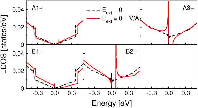

Fig. 15 shows the LDOS for the bilayer near the Fermi energy. The chemical charge transfer (for vanishing field) from atoms A1+ and B1+ to A3+ and B2+ (see Fig. 14 and Table 1) is reflected in the fact that the LDOS below the Fermi level for the atoms with excess charge (A3+ and B2+) is much higher than for the deficit atoms (A1+ and B1+). An electric field changes the analytical properties of the energy bands qualitatively: the cusps turn into Mexican hat structures, Fig. 3. Because the iso-energy lines of the extrema are roughly speaking circles, which resembles a one-dimensional band structure, the total DOS (sum of all LDOS) must exhibit -type singularities at the edges of the gap Guinea et al. (2006). The intuitive guess that the singularity at the occupied side of the gap should appear in the LDOS of atom A3+ and the singularity at the unoccupied side of the gap on atom B2+ is confirmed by the calculation. Both atoms have dangling -bonds toward the interior of the slab. The occupied peak at A3+ is connected with the physical charge accumulation at the A3+ atom (see Table 1) in the electric field.
Fig. 16 shows the LDOS of the ABCAB slab. The LDOS of the surface atoms of this stack is expected to show virtually the features of an infinitely thick slab. Despite the fact that Fig. 16 shows much more singularities and structures than the bilayer due to the more complicated band structure, the LDOS of the surface atoms near the Fermi energy in the electric field is very similar to the bilayer: the LDOS at the band edges of the surface atoms with dangling bonds have singularities and the LDOS of the other surface atoms is very small. This is partly due to the fact that the energy bands in the external field in the vicinity of the Fermi energy shown in Fig. 3 are similar: all exhibit a Mexican hat shape. These singularities at the band edges are still observable in a weaker form at atoms with inward pointing dangling bonds, which are located in the second layer below the surfaces (B1+ and A1-). As a rule, the singularities are located on the occupied side of the gap in the negatively charged layers and on the unoccupied side of the gap for positively charges layers (see Figs. 14 and 16). As shown in Mak et al. (2010) for the 4-layer system, the corresponding singularities in the joint density of states are clearly seen in infra-red absorption spectra and can be used to identify the stacking order of stacks prepared by exfoliation.
III.8 Dielectric constant
We are aware of the fact that a general response relation in inhomogeneous systems should include nonlocal effects,
| (4) |
Therefore, for the extraction of the full information about the dielectric response function from a finite field calculation we had to apply -dependent external fields . The local field corrections included in Eq. (4) imply that even for a constant external field the internal field is -dependent. Because it is numerically extremely difficult to extract the full information about from a finite field approach, we here use a mesoscopic description by a dielectric constant (DC) which is independent of within the slab. To this end, we follow macroscopic electrodynamics and determine a spatially averaged internal field from
| (5) |
where is the dipole moment per volume, induced by the homogeneous external field . For the definition of the volume of the -layer slab we used a thickness of . Thus, . We consider only the -components of , , and , since by symmetry the other components are zero.
The next point to note is that the gap was found to be strongly dependent on the strength of , see Fig. 7. This implies that also should be strongly field dependent. Thus, we take a differential definition,
| (6) |
The more commonly used alternative of a power expansion of in with field-independent expansion coefficients is not suited for strong nonlinearities, in particular in cases like ours where the gap depends strongly on the external field and for vanishing field the system is (semi)metallic.
In order to establish a relation with Eq. (5), we define an averaged DC via integration of Eq. (6),
| (7) |
Using Eq. (5), we find
| (8) |
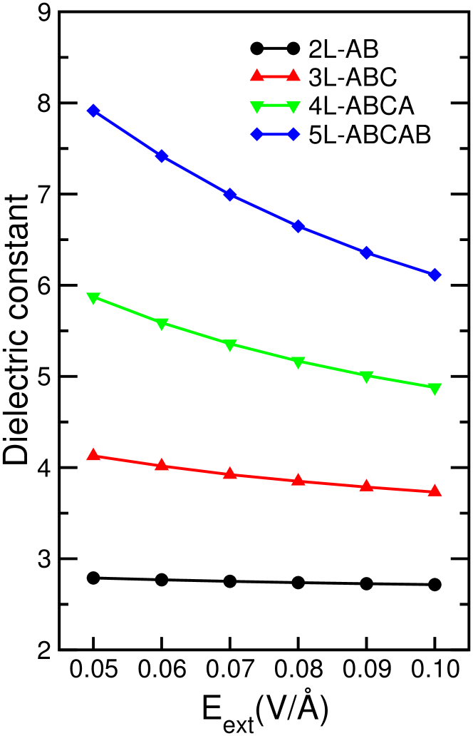
Despite the somewhat loose connection to the fully non-local dielectric response function, provides exact information about the induced dipole moment per surface area.
As seen in Fig. 17, decreases with increasing . This trend can be understood from the fact that the gap width grows monotonously with the external field in the considered field range, Fig. 7. Another trend also seen in Fig. 17 is the increase of with increasing number of layers for fixed external field. For this trend can be qualitatively explained with the same argument as before, since the gap width decreases with increasing . Obviously the opening of a gap by an external field is the harder the thicker the slab is. The bilayer is an exception, because in this system there is no next-neighbor inter–layer interaction.
An interesting application is offered by the distinct values of for a relatively large range of external field values. Namely, a measurement of should allow to discriminate the number of layers and, perhaps, also the stacking type. Such a discrimination was only recently achieved by synchrotron-based infrared absorption-spectroscopy Mak et al. (2010).
We should finally mention the small absolute value for the DC of the bilayer system, about 2.7 in the considered field range. This is well below the value for , , and might be relevant for fast nano- or molecular electronics.
IV Summary and Conclusions
We performed a DFT investigation of the electronic structure and of
the electric-field response of (ABC)-stacked graphene slabs with
finite thickness. For comparison, related calculations were carried
out for single layer graphene, AB-bilayer, 5-layer and 6-layer
(AB)-slabs. Further, the electronic structure of bulk -graphite
was clarified.
The main results can be summarized as follows:
(i) The ABC-trilayer is a zero-gap semi-conductor,
but all other (ABC) slabs up to 10
layers thickness and also bulk (ABC) graphite (-graphite)
are semi-metals.
Thus, very probably all (ABC)-slabs with more than 3 layers
are semi-metallic.
(ii) We confirmed that in (ABC) slabs up to at least 10
layers thickness
only surface states are located at the Fermi energy
and provided a topological argument based on a tight-binding Hamiltonian
that this should hold for layer thickness larger than 10 as well.
This means, that electronic transport parallel to
such slabs is confined to a surface region.
Another, more general implication arising from our
topological argument is that
conducting zero-energy modes also should appear at
grain boundaries between (AB) and (ABC) stacking
and at domain walls separating (ABC) from (CBA)
regions. Since finite-thickness (ABC) stacking is
common both in natural and in synthesized graphite, the electric
conductance of graphite should be very sensitive to
the specific amount of stacking domain walls
and grain boundaries.
(iii) The band structure of the AB-bilayer has been thoroughly
revisited. We found on the meV-scale a tiny electron pocket around
the K-point and a hole pocket on the line K- close to K.
Thus, already an undoped AB-bilayer has a finite Fermi line,
in contrast to results from tight-binding calculations with
up to three hopping parameters and in agreement with other
DFT results.
We found that meV-features and the topology of
the Fermi surfaces are very delicate.
Thus, tight-binding results using overlap parameters from
bulk graphite may on the low-energy scale considerably differ
from self-consistent DFT results.
(iv) Band structures of several few-layer (ABC) slabs
and of bulk (ABC) graphite were presented and critically
compared with available literature data.
The low-energy band structure of bulk -graphite
consists of two Dirac-like cones above and
below the Fermi level with an energy distance of 9 meV.
Since for few-layer (ABC) slabs there is a gap
in the bulk-like states, we conclude that
there is a critical thickness
beyond which (ABC) slabs are bulk semi-metallic.
(v) (ABC)-stacked graphene systems with
layers were found to open a band gap in external electric fields,
which increases with the electric field strength
in the considered range up to 0.1 V/Å.
(vi) The strong electric-field dependence of the
electronic structure of (ABC) slabs yields a related field dependence
of the dielectric response. A properly defined field-averaged
dielectric constant decreases with increasing
external field.
Both the band gap and the dielectric constant are
determined by the number of graphene layers and
systems with different numbers of layers show different
tuning ratios for the
dielectric constant.
These properties provide a chance to choose a specific
graphene system according to application requirements.
Vice versa, the specific dielectric response can be
used to identify the number of layers in (ABC) stacks
and, perhaps, even be used to discriminate the stacking sequence.
(vii) The AB-bilayer shows a remarkably small
value of the static dielectric constant of about .
So small a value might be of interest for
fast nano- or molecular electronics.
(viii) Although not investigated quantitatively in this paper,
it is obvious that in (ABC) slabs the strong dependence of the gap on the
perpendicular field will lead to
a strong dependence of the conductivity parallel to the layer
on the perpendicular field.
(ix) The local density of states was presented both for the
AB-bilayer and for an ABCAB-stack.
This information can be useful for the identification
of a certain stack by infrared absorption spectroscopy.
(x) We found that
the screening properties of finite-thickness graphene stacks resemble
neither those of traditional metals nor those of traditional insulators.
For the AB-bilayer, the inter-layer charge transfer and
the induced atomic intra-layer dipole moments
contribute nearly equally to the total induced dipole moment.
In the thicker slabs, the screening charge per layer induced
by an external
field shows a rapid decay toward the interior of the slab.
More than of the induced charge is located
in the very surface layers, where it is distributed roughly equally
over the lattice sites within the layer cell.
On the other hand, the induced intra–layer dipole
moments decay on a much larger length-scale.
The latter contribution is not included in simplified
screening models.
Consequently, such models can provide only qualitative
results.
(xi) Whereas (ABC)-stacked slabs show chemical charge transfer
only near the surface, in the (AB) stacks this transfer
is largest in the interior and decreases toward the surface.
The electrons are transfered from the atoms with saturated bonds
toward atoms with dangling bonds.
As a bottom line, we note that (ABC) stacks rather than (AB) stacks with more than two layers may turn out to be of potential interest for applications relying on the tunability of electronic properties by an external electric field. Such slabs with rhombohedral stacking have non-metallic bulk-like states up to a large critical thickness and topologically protected zero-energy surface states. Thus, they open a tunable gap in an external field which can additionally be tailored by the choice of the layer thickness. Beyond this practical aspect, many interesting features are expected both for pure -graphite micro-crystals as well as for graphite with controlled embeddings of (ABC) stacks.
V Acknowledgements
We gratefully acknowledge discussions with Helmut Eschrig, with Jeroen van den Brink, and with Ulrike Nitzsche. Financial support was provided by Deutsche Forschungsgemeinschaft via grant RI932/6-1.
References
- Novoselov et al. (2004) K. S. Novoselov, A. K. Geim, S. V. Morozov, D. Jiang, Y. Zhang, S. V. Dubonos, I. V. Grigorieva, and A. A. Firsov, Science 306, 666 (2004).
- Castro Neto et al. (2009) A. H. Castro Neto, F. Guinea, N. M. R. Peres, K. S. Novoselov, and A. K. Geim, Rev. Mod. Phys. 81, 109 (2009).
- Oostinga et al. (2008) J. B. Oostinga, H. B. Heersche, X. Liu, A. F. Morpurgo, and L. M. K. Vandersypen, Nature Mater. 7, 151 (2008).
- Karpan et al. (2007) V. M. Karpan, G. Giovannetti, P. A. Khomyakov, M. Talanana, A. A. Starikov, M. Zwierzycki, J. van den Brink, G. Brocks, and P. J. Kelly, Phys. Rev. Lett. 99, 176602 (2007).
- Nomura and MacDonald (2006) K. Nomura and A. H. MacDonald, Phys. Rev. Lett. 96, 256602 (2006).
- Zhou et al. (2007) S. Y. Zhou, G.-H. Gweon, A. V. Fedorov, P. N. First, W. A. de Heer, D.-H. Lee, F. Guinea, A. H. Castro Neto, and A. Lanzara, Nature Mater. 6, 770 (2007).
- Giovannetti et al. (2007) G. Giovannetti, P. A. Khomyakov, G. Brocks, P. J. Kelly, and J. van den Brink, Phys. Rev. B 76, 073103 (2007).
- Ohta et al. (2006) T. Ohta, A. Bostwick, T. Seyller, K. Horn, and E. Rotenberg, Science 313, 951 (2006).
- McCann (2006) E. McCann, Phys. Rev. B 74, 161403(R) (2006).
- Castro et al. (2007) E. V. Castro, K. S. Novoselov, S. V. Morozov, N. M. R. Peres, J. M. B. Lopes dos Santos, J. Nilsson, F. Guinea, A. K. Geim, and A. H. Castro Neto, Phys. Rev. Lett. 99, 216802 (2007).
- Min et al. (2007) H. Min, B. Sahu, S. K. Banerjee, and A. H. MacDonald, Phys. Rev. B 75, 155115 (2007).
- Latil and Henrard (2006) S. Latil and L. Henrard, Phys. Rev. Lett. 97, 036803 (2006).
- Aoki and Amawashi (2007) M. Aoki and H. Amawashi, Solid State Commun. 142, 123 (2007).
- Min and MacDonald (2008) H. Min and A. H. MacDonald, Phys. Rev. B 77, 155416 (2008).
- Guinea et al. (2006) F. Guinea, A. H. Castro Neto, and N. M. R. Peres, Phys. Rev. B 73, 245426 (2006).
- Koshino (2010) M. Koshino, Phys. Rev. B 81, 125304 (2010).
- Lipson and Stokes (1942) H. Lipson and A. R. Stokes, Proc. R. Soc. A 181, 101 (1942).
- Partoens and Peeters (2006) B. Partoens and F. M. Peeters, Phys. Rev. B 74, 075404 (2006).
- Lu et al. (2006) C. L. Lu, C. P. Chang, Y. C. Huang, J. M. Lu, C. C. Hwang, and M. F. Lin, J. Phys.: Condens. Matter 18, 5849 (2006).
- Zhang et al. (2010) F. Zhang, B. Sahu, H. Min, and A. H. MacDonald, Phys. Rev. B 82, 035409 (2010).
- Mak et al. (2010) K. F. Mak, J. Shan, and T. F. Heinz, Phys. Rev. Lett. 104, 176404 (2010).
- Cousins (2003) C. S. G. Cousins, Phys. Rev. B 67, 024110 (2003).
- Charlier et al. (1994) J.-C. Charlier, X. Gonze, and J.-P. Michenaud, Carbon 32, 289 (1994).
- Kunc and Resta (1983) K. Kunc and R. Resta, Phys. Rev. Lett. 51, 686 (1983).
- Neugebauer and Scheffler (1992) J. Neugebauer and M. Scheffler, Phys. Rev. B 46, 16067 (1992).
- Bengtsson (1999) L. Bengtsson, Phys. Rev. B 59, 12301 (1999).
- (27) http://www.fplo.de/.
- F.Tasnádi (2007) F.Tasnádi, J. Comput. Theor. Nanosci. 4, 1206 (2007).
- (29) http://www.flapw.de/.
- Koepernik and Eschrig (1999) K. Koepernik and H. Eschrig, Phys. Rev. B 59, 1743 (1999).
- Perdew and Wang (1992) J. P. Perdew and Y. Wang, Phys. Rev. B 45, 13244 (1992).
- not (a) While general agreement about the in-plane lattice constant of graphite exists, different values of the layer distance are found in the literature; here, the value taken in ref. Aoki and Amawashi, 2007, which is close to the exprimental low-temperature value of 3.336 å Baskin and Meyer (1955), was used.
- (33) http://www.quantum-espresso.org/.
- Giannozzi et al. (2009) P. Giannozzi, S. Baroni, N. Bonini, M. Calandra, R. Car, C. Cavazzoni, D. Ceresoli, G. L. Chiarotti, M. Cococcioni, I. Dabo, et al., J. Phys.: Condens. Matter 21, 395502 (2009).
- Zhang et al. (2009) Y. Zhang, T.-T. Tang, C. Girit, Z. Hao, M. C. Martin, A. Zettl, M. F. Crommie, Y. R. Shen, and F. Wang, Nature 459, 820 (2009).
- Yu et al. (2008) E. K. Yu, D. A. Stewart, and S. Tiwari, Phys. Rev. B 77, 195406 (2008).
- Hybertsen and Louie (1986) M. S. Hybertsen and S. G. Louie, Phys. Rev. B 34, 5390 (1986).
- Koshino and McCann (2009) M. Koshino and E. McCann, Phys. Rev. B 80, 165409 (2009).
- McCann and Fal’ko (2006) E. McCann and V. I. Fal’ko, Phys. Rev. Lett. 96, 086805 (2006).
- Lemonik et al. (2010) Y. Lemonik, I. L. Aleiner, C. Toke, and V. I. Fal’ko (2010), arXiv:1006.1399.
- Su et al. (1979) W. P. Su, J. R. Schrieffer, and A. J. Heeger, Phys. Rev. Lett. 42, 1698 (1979).
- Jackiw and Rebbi (1976) R. Jackiw and C. Rebbi, Phys. Rev. D 13, 3398 (1976).
- not (b) In both cases one component of the vector is zero, which is a strict requirement for the possibility of non-trivial topology.
- Baskin and Meyer (1955) Y. Baskin and L. Meyer, Phys. Rev. 100, 544 (1955).