Many-body effects in van der Waals-Casimir interaction between graphene layers
Abstract
Van der Waals-Casimir dispersion interactions between two apposed graphene layers, a graphene layer and a substrate, and in a multilamellar graphene system are analyzed within the framework of the Lifshitz theory. This formulation hinges on a known form of the dielectric response function of an undoped or doped graphene sheet, assumed to be of a random phase approximation form. In the geometry of two apposed layers the separation dependence of the van der Waals-Casimir interaction for both types of graphene sheets is determined and compared with some well known limiting cases. In a multilamellar array the many-body effects are quantified and shown to increase the magnitude of the van der Waals-Casimir interactions.
I Introduction
Graphene appears to be the only known mono-atomic two-dimensional (2D) crystal and apart from the intrinsic interest it engenders, it is becoming more and more also a focus of possible and desired advanced technological applications Novoselov . It is for these reasons that in the past several years we have witnessed a veritable explosion of theoretical and experimental interest in graphene Novoselov2 . The Nobel prize for physics in 2010 only consolidated this trend. Graphene differs fundamentally from other known 2D semiconductors because of its unique electronic band structure, viz. the monoatomic sheet of carbon atoms arranged in a honeycomb lattice leads to an electron band structure that displays quite unusual properties Electronic . The Fermi surface is reduced to just two points in the Brillouin zone and the value of the band gap is reduced to zero. The energy dispersion relation for both the conduction and the valence bands are linear at low energy, namely less than 1 eV, meaning that the charge carriers behave as relativistic particles with zero rest mass. The agent responsible for many of the interesting electronic properties of graphene sheets is the non-Bravais honeycomb-lattice arrangement of carbon atoms, which leads to a gapless semiconductor with valence and conduction -bands.
States near the Fermi energy of a graphene sheet are described by a massless Dirac equation which has chiral band states in which the honeycomb-sublattice pseudospin is aligned either parallel or opposite to the envelope function momentum. The Dirac-like wave equation leads to both unusual electron-electron interaction effects and to unusual response to external potentials. When the graphene sheet is chemically doped with either acceptor or donor impurities its carrier mobility can be drastically decreased Doped . Because of its 2D periodic structure graphene is closely related to single wall carbon nanotubes, being in fact a carbon nanotube rolled out into a single 2D sheet Saito . The main difference between the electronic properties of single wall carbon nanotubes and graphene is that the former show circumferential periodicity and curvature that leave their imprint also in the electronic spectrum and consequently also van der Waals (vdW) interactions Rajter1 ; Rajter2 .
On the other hand, graphite appears to be the poor cousin of graphene though it is the stable form of carbon at ordinary temperatures and pressures. Many efforts have been invested into understanding its structural and electronic details (for an account see Ref. Graphitecalcs ). Various known modifications of graphite differ primarily in the way the mono-atomic two-dimensional graphene layers stack. Their stacking sequence in terms of commonality is ABA for the Bernal structure, AAA for simple hexagonal graphite or ABC for the rhombohedral graphite Graphite .
Graphene layers in graphitic systems are basically closed shell systems and thus have no covalent bonding between layers which makes them almost a perfect candidate to study long(er) ranged non-bonding interactions. Indeed, they are stacked at an equilibrium interlayer spacing of about 0.335 nm and are held together primarily by the non-bonding long range vdW interactions GraphitevdW . Therefore the interaction between graphene layers can be described as a balance between attractive vdW dispersion forces and corrugated repulsive (Pauli) overlap forces Crespi , following in this respect closely the paradigm of nano-scale interactions Rudi-RMP-2010 .
Besides a few notable exceptions earlymanybodyeffects , until 2009 many electronic and optical properties of graphene could be explained within a single-particle picture in which electron-electron interactions are completely neglected. The discovery of the fractional quantum Hall effect in graphene fqhe represents an important hallmark in this context. By now there is a large body of experimental work eeinteractionsgraphene ; bostwick_science_2010 ; kotov_arXiv_2010 showing the relevance of electron-electron interactions in a number of key properties of graphene samples of sufficiently high quality.
Because of band chirality, the role of electron-electron interactions in graphene sheets differs in some essential ways Asgari-MacDonald-PRL ; ourdgastheory ; dassarmadgastheory from the role which it plays in an ordinary 2D electron gas. One important difference is that the contribution of exchange and correlation to the chemical potential is an increasing rather than a decreasing function of carrier density. This property implies that exchange and correlation increases the effectiveness of screening, in contrast to the usual case in which exchange and correlation weakens screening dft . This unusual property follows from the difference in sublattice pseudospin chirality between the Dirac model’s negative energy valence band states and its conduction band states Asgari-MacDonald-PRL ; ourdgastheory , and in a uniform graphene system is readily accounted for by many-body perturbation theory.
In this work we focus our efforts on the vdW dispersion component of the graphene stacking interaction. Dispersion forces can be formulated on various levels vdWgeneral giving mostly consistent results for their strength and separation dependence. In the context of graphene stacking interactions, the problem can be decomposed into the calculation of the dielectric response of the carbon sheets and the subsequent calculation of the vdW interactions either via the quantum-field-theory-based Lifshitz approach, as advocated in this paper, by means of the electron correlation energy Sernelius or the non-local vdW density functional theory Rydberg . One can show straightforwardly that in fact the non-local van der Waals functional approach of the density functional theory and the Lifshitz formalism are in general equivalent Veble .
Specifically we will calculate the vdW-Casimir interaction free energy, per unit area between two graphene sheets as a function of the seperation between them, in a system composed of
-
a)
two apposed undoped or doped graphene sheets,
-
b)
an undoped or a doped graphene layer over a semi-infinite substrate, and
-
c)
a multilayer (infinite) array of graphene sheets.
In the latter case we will investigate the many-body non-pairwise additive effects in the effective interaction between two sheets within a multilayer array. We should note that non-pairwise additive effects are ubiquitous in the context of vdW interactions vdWgeneral often leading to non-trivial properties of macromolecular interactions. In this case they will lead to variations in the equilibrium stacking separation as a function of the number of layers in a graphitic configuration. In the calculation of the vdW-Casimir free energy we will employ the dielectric response function of a single graphene layer calculated previously Asgari-MacDonald-PRL .
II vdW-Casimir interaction between two layers of graphene
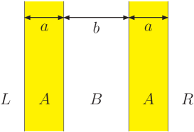
The geometry of the system composed of two parallel graphene layers with thicknesses , facing each other in a bilayer arrangement at a separation , is shown schematically in Fig. 1. In view of later generalizations we label the left semi-infinite vacuum space as , graphene sheets as , the intervening layer as and the right semi-infinite vacuum space by .
In order to calculate the vdW-Casimir dispersion interaction free energy in the planar geometry we use the approach of Ref. Rudi-JCP-119-1070-2003 where it has been calculated exactly for a multilayer planar geometry. The thus derived general form of the interaction free energy per unit area includes retardation effects and is therefore valid for any spacing between the layers.
For the system which is shown schematically in Fig. 1, the vdW-Casimir interaction free energy is obtained in the Lifshitz form as
| (1) |
where stands for the graphene-graphene interaction free energy as a function of the layer spacing (normalized in such a way that it tends to zero at infinite interlayer separation). In the above Lifshitz formula the summation is over the transverse wave vector and the summation (where the prime indicates that the term has a weight of ) is over the imaginary Matsubara frequencies
| (2) |
where is the Boltzman constant, is the absolute temperature, and is the Planck constant devided by . All the quantities in the bracket depend on as well as .
The other quantities entering the Lifshitz formula are defined as
| (3) | |||||
with
| (4) |
where quantifies the dielectric discontinuity between homogeneous dielectric layers in the system, where a layer labeled by is located to the left hand side of the layer labeled by (for details see Ref. Rudi-JCP-119-1070-2003 ). Also for each electromagnetic field mode within the material is given by
| (5) |
where is the speed of light in vacuo, is the magnitude of the transverse wave vector, and and are the dielectric function and the magnetic permeability of the -th layer at imaginary frequencies, respectively. For the sake of simplicity we assume that for all layers and that the dielectric function for vacuum layers equals to for all frequencies.
Note that is standardly referred to as the vdW-London transform of the dielectric function and is defined via the Kramers-Kronig relations as Wooten
| (6) |
It characterizes the magnitude of spontaneous electromagnetic fluctuations at frequency . In general is a real, monotonically decaying function of the imaginary argument (for details see Parsegian’s book in Ref. vdWgeneral ).
In order to proceed one needs the vdW-London transform of the dielectric function of all layers in the system. The detailed - and -dependent form of the dielectric function for undoped and/or doped graphene layers are introduced in Secs. II.1 and II.2.
II.1 Two undoped graphene layers
We employ the response function of a graphene layer from Refs. Asgari-MacDonald-PRL ; others which for doped graphene assumes the form
| (7) | |||||
where , is the Fermi velocity in graphene layer and is the chemical potential, the Fermi energy, and is the Fermi momentum, where and is the the average electron density.
To begin with, we assume that two layers are decoupled and ignore the interlayer Coulomb interaction. The vdW-London dispersion transform of the dielectric function on the level of the random phase approximation (RPA) is then given by
| (8) |
where is the (transverse) 2D Fourier-Bessel transform of the Coulomb potential, , is the electric charge of electron, is the permittivity of the vacuum and is the average of the dielectric constant for the surrounding media which is equal to 1 for vacuum. In what follows we furthermore assume that to the lowest order the dielectric properties of the graphene layers are not affected by the variation of the separation between them. This assumption is also consistent with the Lifshitz theory that presumes complete independence of the dielectric response functions of the interacting layers.
For undoped graphene layer, i.e. , the expression for the vdW-London dispersion transform of the dielectric function simplifies substantially and assumes the form
| (9) |
where is the electromagnetic fine-structure constant . It should be noted that, in general, a model going beyond the RPA is necessary in order to account for enhanced correlation effects that would be present in an undoped system LA . In this paper, however, we restrict ourselves to the RPA approximation and analyze its predictions in detail.
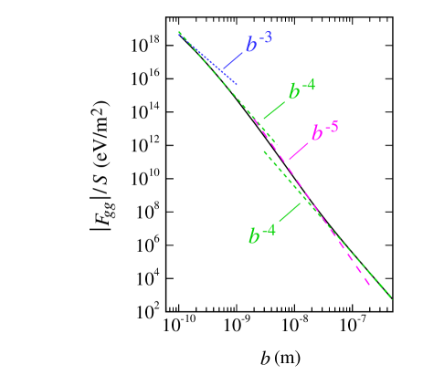
The functional dependence of the interaction free energy of the system per unit area, Eq. (1), is presented in Fig. 2 as a function of the separation between two graphene layers. We assume that the graphene layers are immersed in vacuo and both of them have the same thickness Å as well as equal susceptibilities. Note that in all cases considered in this paper the interaction free energies as defined in Eq. (1) are negative reflecting attractive vdW-Casimir force between graphene layers in vacuum. For the sake presentation, we shall plot the absolute value (magnitude) of the free energy in all cases.
As one can discern from Fig. 2 the general dependence of the vdW-Casimir interaction free energy on the separation between the graphene layers has the scaling form of a power law, , with a weakly varying separation-dependent scaling exponent, . This scaling exponent can be defined standardly as vdWgeneral
| (10) |
For two undoped graphene sheets we observe that at small separations the functional dependence of the free energy on interlayer spacing yields the scaling exponent for smallest values of the separation. The scaling exponent then steadily increases to , then , and finally at asymptotically large separations it reverts back to . This variation in the scaling exponent for the separation dependence of the interaction free energy can be rationalized by invoking some well known results on the vdW interaction in multilayer geometries (see e.g. the relevant discussions in Ref. vdWgeneral ).
For example, for two semi-infinite layers the interaction free energy should go from the non-retarded form characterized by for small spacings, through retarded form for larger spacings and then back to zero-frequency-only form that also scales with but with a different prefactor than the non-retarded form. For two infinitely thin sheets, on the other hand, we have the non-retarded form for small separation, followed by the retarded form for larger spacings and then reverting back to zero-frequency-only term with scaling, but again with a different prefactor than the non-retarded limit. Furthermore, the transitions between various scaling forms and the locations of the transition regions are not universal but depend crucially on the characteristics of the dielectric spectra and can thus be quite complicated, sometimes not yielding any easily discernible regimes with a quasi-constant scaling exponent .
Reading Fig. 2 with this in mind we can come up with the following interpretation of the calculated separation dependence: for small separation the interaction free energy is dominated by the dependence except in the narrow interval very close to vanishing separation where the dependence asymptotically levels off at form. This form is consistent with the non-retarded interaction between two very thin layers, see above, for small but not vanishing separations. For vanishing interlayer separations the final leveling-off of the scaling exponent is due to the fact that the system is approaching the limit of two semi-infinite layers where in principle , but in reality the finite thickness of the graphene sheets is way too small to observe this scaling in its pure form. All we can claim is that for vanishing interlayer spacings the scaling exponent drops below the value, valid for two infinitely thin layers.
For larger values of the interlayer separations we then enter the retarded regime with scaling exponent, again valid strictly for two infinitely thin layers. The retarded regime finally gives way to the regime of asymptotically large spacings where the interaction free energy limits towards its form given by the zero frequency term in the Matsubara summation and characterized by scaling dependence. Obviously the numerical coefficient in the small separation non-retarded and asymptotically large separation regimes (both with ) are necessarily different.
The interaction free energy scaling with the interlayer separation is thus completely consistent with the vdW-Casimir interactions between two thin dielectric layers for all, except for vanishingly small, separations where finite thickness effects of the graphene sheets leave their mark in a smaller value of the scaling exponent that should ideally approach the value valid for a regime of interaction between two semi-infinite layers.
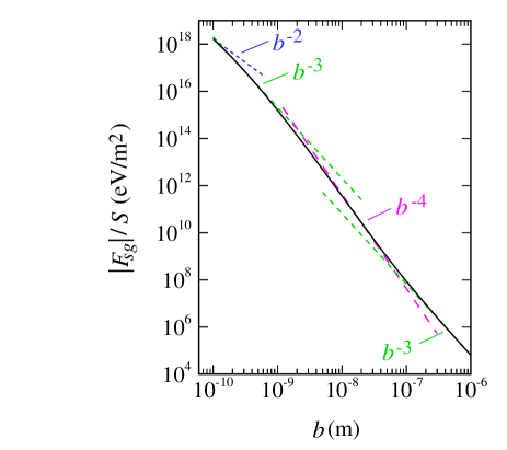
The numerical value of the interaction free energy per unit area at is about . That means that for two graphene layers with surface area of the magnitude of the free energy is about at 1 nm separation; at it is about and at about for the same surface area.
II.2 Two doped graphene layers
For a doped graphene layer the vdW-London dispersion transform of the dielectric function can be read off from Eqs. (8) and (7) as
| (11) | |||||
with the following coefficients
| (12) |
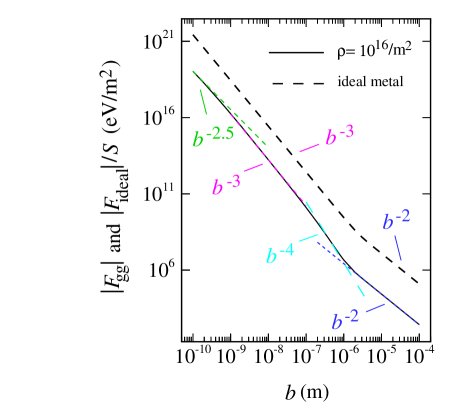
With this dielectric response function we again evaluate the vdW-Casimir interaction free energy of the system per unit area, Eq. (1), as a function of the separation between two graphene layers as shown in Fig. 3. The interaction free energy has again a scaling form with a scaling exponent varying with the separation between the layers. It is clear that in this case it is much more difficult to partition the variation of the scaling exponent into clear-cut piecewise constant regions.
As it can be seen from Fig. 3 at small separations the form of the functional dependence of the interaction free energy has . Then for increasing spacings there follows a relatively broad regime with , followed eventually by the scaling form with for . One needs to add here that only the scaling regime of for asymptotically large separations and an intermediate regime with are clearly discernible.
We can gain some understanding of these regimes by comparing with the various exact limits in the layer geometry as before. Such comparison is however not as straightforward as before. The asymptotic regime is easiest to rationalize: it has the same scaling form as the finite temperature vdW-Casimir interaction between two metallic sheets at asymptotically large separations. The presence of free charges would in fact be a reasonable characterization of doped graphene layers. For smaller separations we then enter the regime dominated by the retardation effects with form, and finally for vanishing separations we approach the regime of . Recent calculations of vdW interactions between thin metallic layers indeed lead to exactly this exponent for small layer separations sernelius2 . The doped graphene sheet results would thus indicate that the dependence of the vdW-Casimir interactions free energy on the separation could be rationalized in terms of interactions between two thin metallic sheets.
For comparison we have also plotted the interaction free energy between two ideal metallic sheets which exhibits a much stronger attractive interaction free energy, i.e. vdWgeneral
The numerical value of the energy per unit area at is about which is equal to for surface area of ; at it is about and at it is about for the same surface area.

II.3 Doped vs. undoped graphene
It is instructive to compare the interaction between two graphene layers in the undoped and doped cases. For this purpose we have plotted the interaction free energy of the system for both cases in Fig. 4. The electron density in doped graphene is assumed to be (solid curve). The dashed curve is the interaction free energy of the system composed of two undoped graphene layers. As it can be seen, for all separations the magnitude of the interaction free energy for doped graphene layers is more than that of the undoped one (note again that the interaction free energies as defined in Eq. (1) are negative in the present case due to attractive vdW-Casimir force between graphene layers in vacuum). At separation the vdW-Casimir interactions for doped graphene is about 30 times the magnitude of the interaction for undoped graphene, while at the separation of this ratio is about 1600. This means that the attractive interaction between graphene layers is enhanced when the contribution of the electron density in the dielectric function of the graphene layers is taken into account. This same trend was observed also in the work of Sernelius Sernelius and is clearly a consequence of the fact that the largest value of vdW-Casimir interactions is obtained for ideally polarizable, i.e. metallic layers. The closer the system is to this idealized case, the larger the corresponding vdW-Casimir interaction will be.
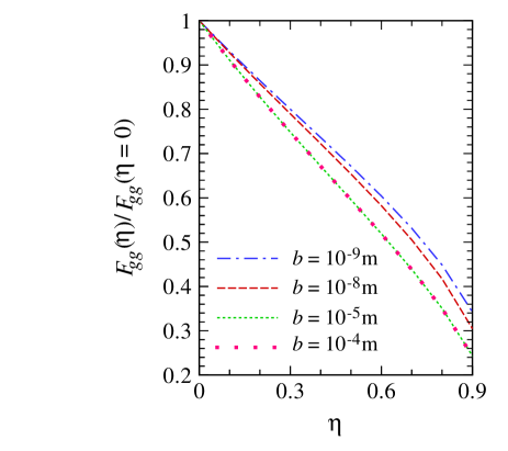
Let us investigate also the effect of asymmetry of doped graphene sheets on vdW-Casimir interactions between them. Introducing the dimensionless parameter , where is the electron density of the -th graphene layer (), we find that the interaction free energy depends on the asymmetry in the system. When , the electron densities are the same for both graphene layers and we have a symmetric case, whereas means that one of the graphene layers is undoped while the other one is doped, leading to an asymmetric case. In Fig. 5 we have plotted the rescaled free energy of the system composed of two graphene layers as a function of for different values of the interlayer separation. The magnitude of the electron density for one of the layers has been fixed at while that of the other layer, , varies. As seen from this figure, the curves show a monotonic dependence on with a stronger interaction at smaller values of . Note that at large separations the curves tend to coincide and will become indistinguishable. The asymmetry effects are therefore largest at small separations between the interacting graphene layers.

II.4 Hamaker coefficient for two graphene layers
The general form of the Hamaker coefficient, , for a system composed of two dielectric layers of finite thickness (Fig. 1) when retardation effects are neglected is defined via vdWgeneral
| (14) |
At large separations , the Hamaker coefficient, , can be obtained from
| (15) |
while at small separations , it can be read off from
| (16) |
In Fig. 6, we show the Hamaker coefficient as a function of the layer separation for a system of two undoped graphene layers. We show the general form of the Hamaker coefficient from Eq. (14) (solid line) as well as the limiting forms at small (dotted line, Eq. (16)) and large (dashed line, Eq. (15)) separations. The large-distance limiting form obviously coincides with the general form at separations beyond . The small-distance limiting form tends to the general form at small separations but given that the thickness of the layers is only about Å, it is expected to merge with the general form in sub-Ångström separations. For doped graphene, a similar analysis to Eq. (14) is not possible because the corresponding general expression for the interaction free energy is missing.
III vdW-Casimir interaction between a graphene layer and a semi-infinite substrate
In this section we study the interaction between a graphene layer and a semi-infinite dielectric substrate as depicted schematically in Fig. 7. For this system the free energy per unit area is
where now stands for the interaction free energy between the substrate and the graphene layer. We have excluded the explicit dependence of the quantities in the bracket on the imaginary Matsubara frequencies, but they are the same as in Eq. (4).
In order to gain insight into the magnitude of the vdW-Casimir interaction free energy and for the sake of simplicity, we assume that the semi-infinite substrate is made of SiO2 which has the vdW-London dispersion transform of the dielectric function of the form Ninham-Mahanty-Book ; vdWgeneral
| (18) |
where the values of the parameters, CUV = 1.098, CIR = 1.703, rad/s, and rad/s have been determined from a fit to optical data Hough . The static dielectric permittivity of SiO2 is then obtained as . A characteristic feature of the vdW-London transform of SiO2 is thus that it contains two relaxation mechanisms. The first one is due to electronic polarization and the second one is due to ionic polarization. All calculations of the vdW-Casimir interaction free energy are done at room temperature ().
III.1 Undoped graphene apposed to a substrate
Using the vdW-London transforms of the dielectric functions given in the preceding sections, one can now calculate the free energy, Eq. (LABEL:eq:Free-Energy-substrate-and-Graphen-sheet), for an undoped graphene layer next to a semi-infinite SiO2 substrate. The results are shown in Fig. 8.
At small separations, the free energy varies with a scaling exponent , while at larger separations one can distinguish the scaling regimes , and , finally approaching the asymptotic limit at large separations with . This sequence of interaction free energy scalings can be rationalized as follows: at asymptotically large separations we are at the zero-frequency Matsubara term for a semi-infinite layer and a thin sheet. This case is right in between the asymptotically large separation limit for two semi-infinite layers () and two infinitely thin layers (). For smaller spacings we then progressively detect contributions from higher Matsubara terms which lead to scaling exponent that corresponds to a retarded form of the interaction free energy and then for yet smaller spacings the scaling exponent reverts to non-retarded form of the vdW interaction between a semi-infinite substrate and an infinitely thin sheet. For vanishing spacings the finite thickness of the sheet starts playing a role and eventually, we approach the scaling for two semi-infinite layers.
The magnitude of the interaction free energy per unit area at is about . It means that for a system with surface area of this value is about . At it is about and at it is about for the same surface area.

III.2 Doped graphene apposed to a substrate
The vdW-Casimir interaction free energy Eq. (LABEL:eq:Free-Energy-substrate-and-Graphen-sheet) for a system composed of a doped graphene layer next to a semi-infinite SiO2 substrate is shown Fig. 9 for two values of the electron density (dashed line) and (solid line).
At small separations the free energy shows the scaling, while for larger spacings it shows a scaling exponent , approaching the limit for asymptotically large separations. In this respect the case of a thin doped graphene sheet apposed to a semi-infinite substrate is very similar to the case of two thin doped layers, except that the retarded regime covers a smaller interval of spacings. This means that the metallic nature of one of the interacting surfaces is enough to switch the behavior of the interaction free energy completely towards the case of two metallic interacting surfaces. This case has in fact not yet been thoroughly discussed in the literature. The changes in the slope appear to occur at the same values of the interlayer spacing when the electron density decreases (compare dashed and solid curves).
The magnitude of the free energy for the electron density (dashed line) and surface area of at is about , while at it is about , and at is about .
These values increase for larger electron densities, e.g., for (solid line) and the same surface area, the free energy magnitude is at , while it is about at and about at .
III.3 Hamaker coefficient for the graphene-substrate system
The general form of the Hamaker coefficient, , for a system composed of a dielectric layer of finite thickness apposed to a semi-infinite dielectric substrate (Fig. 7) when retardation effects are neglected is defined via vdWgeneral
| (19) |
At large separations , the Hamaker coefficient, , can be obtained from
| (20) |
while at small separations , it can be read off from
| (21) |
In Fig. 10, we again show the Hamaker coefficient as a function of the layer separation for a system comprising a SiO2 substrate and an undoped graphene layer. We show the general form of the Hamaker coefficient from Eq. (19) (solid line) as well as the limiting forms at large (dashed line, Eq. (20)) and small (dotted line, Eq. (21)) separations. The large-distance limiting form obviously coincides with the general form at separations beyond but again since the thickness of the graphene layer is only about Å, the small-distance limiting form is expected to merge with the general form in sub-Ångström separations.
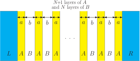
IV vdW-Casimir interaction in a system composed of layers of graphene
In this section we shall use the Lifshitz formalism in order to study the many-body vdW interactions in a system composed of layers of graphene. The layers are separated from each other by layers of vacuum and are bounded at the two ends by two semi-infinite dielectric slabs as depicted in Fig. 11. The thickness of each graphene layer is while the separation between two successive layers is . We have labeled the left semi-infinite dielectric medium with , the right one with (which both will be assumed to be vacuum), the graphene layers with and the vacuum layers with . Following Ref. Rudi-JCP-124-044709-2006 , one can calculate the vdW-Casimir part of the interaction free energy, , in an explicit form for any finite . Interestingly, it turns out that for very large values of the vdW-Casimir free energy can be written as a linear function of so that the interaction free energy becomes Rudi-JCP-124-044709-2006
| (22) |
where can be interpreted as an effective pair interaction between two neighboring layers in the stack and is given by
| (23) | |||||
with defined as
Here is
| (25) |
where and are
| (26) |
For simplicity we have dropped the explicit dependence on the Matsubara frequency in all the above expressions. We stress that is an effective pair interaction between two neighboring graphene layers in a multilayer geometry and is in general not equal to in Eq. (1), which is valid for two interacting layers in the absence of any other neighboring layers. The difference between these two interaction free energies thus encodes the non-pairwise additive effects in the interaction between two layers due to the presence of other vicinal layers.
IV.1 undoped graphene layers
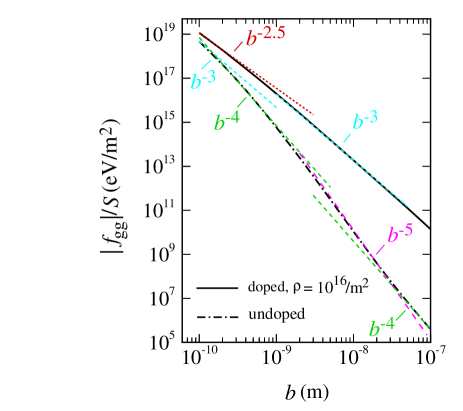
Let us first consider the case of undoped graphene layers. In this case the vdW-Casimir interaction free energy per unit area and per number of layers, (black dot-dashed line), has been plotted in Fig. 12 as a function of the separation between the layers, . The temperature of the system is chosen as , the thickness of the graphene layers is Å and we have used the dielectric function given by Eq. (9) for each undoped graphene sheet.
The value of at is about which is when the surface area is equal to . At the value of for the same surface area is about and at is about .
The scaling of for different values of the interlayer spacing is shown in Fig. 12. It shows the scaling exponent at vanishing separations while at finite yet small separations it is characterised by , continuously merging into a form and finally attaining the form. The rationalization of this sequence of scaling exponents is exactly the same as in the case of two isolated layers and will thus not be repeated here.
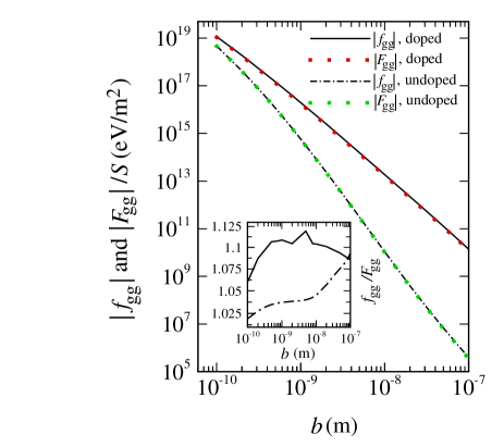
One can directly compare the reduced free energy, , with that of a system composed of only two undoped graphene layers of the same thickness , (i.e., comparing the results in Fig. 2 with the corresponding results in Fig. 12). This is shown in Fig. 13 (black dot-dashed line and green dots), where apparently the results nearly coincide. However, by inspecting the ratio between these two interaction free energies it turns out that in the multilayer system the interaction free energy per layer is slightly more attractive than in the case of a two-layer system. This difference thus stems directly from the many-body effects which in this case augment the binding interaction in a graphitic stack.
IV.2 doped graphene layers
In Fig. 12 the magnitude of the vdW-Casimir interaction free energy for doped graphene layers per unit area and per number of layers, , is plotted (black solid line) as a function of the separation between layers, . The vdW-London dispersion transform of the dielectric function for each graphene sheet is chosen as in Eq. (11). We have fixed the density of electrons for all the graphene layers as . The value of at is about , which is about when the surface area is equal to . At the value of is about and at it is about . The scaling exponents of the interaction free energy dependence for different regions of interlayer spacings are illustrated in Fig. 12. The scaling exponent is for small separations while at larger separations it tends towards the value . It is thus exactly the same as in the case of two isolated doped graphene sheets, see Fig. 3, except that in the multilayer geometry we have not shown the same range of separations as for two isolated layers.
The comparison of vdW-Casimir interaction free energies in the case of two isolated doped graphene sheets with the effective interaction between two graphene sheets in a multilayer system (i.e., comparing in Fig. 3 with in Fig. 12) is made in Fig. 13. As shown by the inset the interaction free energy is again slightly more attractive within a multilayer. Comparing the results in the inset of Fig. 13 shows that in average the many-body effects are stronger in the doped multilayer case than in the undoped case.
Note also that a direct comparison between the undoped and doped systems (Fig. 12) shows that for all separations the free energy magnitude for a doped multilayer (solid line) is more than that of the undoped one (dot-dashed line) and thus the interaction is more attractive in the former case. At separation the magnitude of the doped free energy is about 34 times larger, while at the separation it is about 1730 larger than that of the undoped one.
V Conclusion
In this work we have studied the vdW-Casimir interaction between graphene sheets and between a graphene sheet and a substrate. We calculated the interaction free energy via the Lifshitz theory of vdW interactions that takes as an input the dielectric functions, or better their vdW-London transform, of isolated layers. Within this approach it would be inconsistent to take into account any separation dependent coupling between the dielectric response of the layers. This need possibly not be the case for some other approximate approaches to vdW interactions as in, e.g., the vdW augmented density functional theory (see the paper by Langreth et al. in Ref. vdWgeneral ).
By inserting the random phase approximation dielectric function of a graphene layer into the Lifshitz theory we are thus in a position to evaluate not only the pair interaction between two isolated graphene sheets, but also between a graphene sheet and a semi-infinite substrate of a different dielectric nature (SiO2 in our case) as well as the effective interactions between two graphene sheets in an infinite stack of graphene layers. All these cases that have been analyzed and discussed above are relevant for many realistic geometries in nano-scale systems Rudi-RMP-2010 and thus deserve to be studied in detail.
In the three cases studied we found the following salient features of the vdW-Casimir interaction dependence on the separation between the interacting bodies:
-
1-
In a system composed of two graphene layers we demonstrated that the vdW-Casimir interactions in the case of undoped graphene show scaling exponents identical to those displayed in the case of interacting thin dielectric layers. In the doped case the scaling exponents are consistent with vdW-Casimir interactions between two thin metallic layers.
-
2-
In a system composed of a semi-infinite dielectric substrate and an undoped graphene layer the vdW-Casimir interactions display scaling exponents expected for this asymmetric geometry. For a doped graphene layer the exponents revert to the previous case of two doped graphene layers.
-
3-
In a multilayer system composed of many graphene sheets the vdW-Casimir interaction scaling exponents are the same as in the case of two isolated layers but the interactions are stronger due to many body effects as a consequence of the presence of other layers in a stack.
In order to describe the correlation effects especially at low doping or the interlayer coupling on a more systematic level, one needs to go beyond the standard random phase approximation by incorporating more sophisticated theoretical models for the dielectric response function which would be worth exploring further in the future.
The main motivation for a detailed study of vdW-Casimir interaction between graphene sheets in graphite-like geometries is the fact that graphitic systems belong to closed shell systems and thus display no covalent bonding, so that any bonding interaction is by necessity of a vdW-Casimir type. Its detailed characterization is thus particularly relevant for this quintessential nano-scale system Rudi-RMP-2010 .
VI Acknowledgment
We would like to thank B. Sernelius for providing us with a preprint of his work. R.P. acknowledges support from ARRS through the program P1-0055 and the research project J1-0908. A.N. acknowledges support from the Royal Society, the Royal Academy of Engineering, and the British Academy. J.S. acknowledges generous support by J. Stefan Institute (Ljubljana) provided for a visit to the Institute and the Department of Physics of IASBS (Zanjan) for their hospitality.
References
- (1) K. S. Novoselov, E. McCann, S. V. Morozov, V. I. Fal’ko, M. I. Katsnelson, U. Zeitler, D. Jiang, F. Schedin, A. K. Geim, Nature Phys. 2, 177 (2006).
- (2) A. K. Geim and K. S. Novoselov, Nature Materials 6, 183 (2007).
- (3) A. H. Castro Neto, F. Guinea, N. M. R. Peres, K. S. Novoselov and A. K. Geim, Rev. Mod. Phys. 81, 109 (2009).
- (4) J.-H. Chen, C. Jang, S. Adam, M. S. Fuhrer, E. D. Williams and M. Ishigami, Nature Physics 4, 377 (2008).
- (5) R. Saito, G. Dresselhaus, and M. S. Dresselhaus, Physical Properties of Carbon Nanotubes, 1st Ed. (World Scientific, Singapore, 1998).
- (6) R. F. Rajter, R. Podgornik, V. A. Parsegian, R. H. French, and W. Y. Ching, Phys. Rev. B 76, 045417 (2007).
- (7) A. Šiber, R. F. Rajter, R. H. French, W. Y. Ching, V. A. Parsegian, and R. Podgornik, Phys. Rev. B 80, 165414 (2009).
- (8) M. S. Dresselhaus, G. Dresselhaus, K. Sugihara, I. A. Spain, H. A. Goldberg, Graphite Fibers and Filaments (Springer Series in Materials Science), 1st Ed. (Springer, 1988).
- (9) J.-C. Charlier, X. Gonze, J.-P. Michenaud, Carbon 32, 289 (1994).
- (10) J.-C. Charlier, X. Gonze and J.-P. Michenaud, Europhys. Lett. 28, 403 (1994).
- (11) A. N. Kolmogorov and V. H. Crespi, Phys. Rev. B 71, 235415 (2005); Phys. Rev. Lett 85, 4727 (2000).
- (12) R. H. French, V. A. Parsegian, R. Podgornik et al., Rev. Mod. Phys. 82, 1887 (2010).
- (13) A. Bostwick, T. Ohta, T. Seyller, K. Horn and E. Rotenberg, Nature Phys. 3, 36 (2007); Z. Q. Li, E. A. Henriksen, Z. Jiang, Z. Hao, M. C. Martin, P. Kim, H. L. Stormer and D. N. Basov, Nature Physics 4, 532 (2008).
- (14) X. Du, I. Skachko, F. Duerr, A. Luican and E. Y. Anderia, Nature 462, 192 (2009); K. I. Bolotin, F. Ghahari, M. D. Shulman, H. L. Stormer, P. Kim , Nature 462, 196 (2009).
- (15) V.W. Brar et al., Phys. Rev. Lett. 104, 036805 (2010); E.A. Henriksen et al., ibid 104, 067404 (2010); A. Luican, G. Li, and E.Y. Andrei, Phys. Rev. B83, 041405(R) (2011); K.F. Mak, J. Shan, and T.F. Heinz, Phys. Rev. Lett. 106, 046401 (2011); F. Ghahari et al., ibid 106, 046801 (2011).
- (16) A. Bostwick, F. Speck, Th. Seyller, K. Horn, M. Polini, R. Asgari, A. H. MacDonald, E. Rotenberg, Science 328, 999 (2010).
- (17) V. N. Kotov, B. Uchoa, V. M. Pereira, A. H. Castro Neto, F. Guinea, arXiv:1012.3484.
- (18) Y. Barlas, T. Pereg-Barnea, M. Polini, R. Asgari, and A.H. MacDonald, Phys. Rev. Lett. 98, 236601 (2007).
- (19) M. Polini, R. Asgari, Y. Barlas, T. Pereg-Barnea, and A. H. MacDonald, Solid State Commun. 143, 58 (2007); M. Polini, R. Asgari, G. Borghi, Y. Barlas, T. Pereg-Barnea, and A. H. MacDonald, Phys. Rev. B77, 081411(R) (2008); A. Qauimzadeh, R. Asgari, Phys. Rev. B 79, 075414 (2009); New J. Phys. 11 095023 (2009); A. Qauimzadeh, N. Arabchi and R. Asgari, Solid State Commun. 147, 172 (2008).
- (20) E.H. Hwang and S. Das Sarma, Phys. Rev. B75, 205418 (2007); S. Das Sarma, E.H. Hwang, and W.-K. Tse, Phys. Rev. B75, 121406(R) (2007); E.H. Hwang, B.Y.-K. Hu, and S. Das Sarma, Phys. Rev. B76, 115434 (2007) and Phys. Rev. Lett. 99, 226801 (2007).
- (21) M. Polini, A. Tomadin, R. Asgari, and A. H. MacDonald, Phys. Rev. B 78, 115426 (2008).
- (22) V. A. Parsegian, Van der Waals Forces (Cambridge University Press, Cambridge, 2005); M. Bordag, G. L. Klimchitskaya, U. Mohideen, and V. M. Mostepanenko, Advances in the Casimir Effect (Oxford University Press, New York, 2009); D. C. Langreth et al., J. Phys.: Condens. Matter 21, 084203 (2009); T. Emig, Int. J. Mod. Phys. A 25, 2177 (2010); J. Schwinger, L. L. Deraad, Jr., and K. A. Milton, Ann. Phys. (N.Y.), 115, 1 (1978).
- (23) B. E. Sernelius, arXiv:1011.2363v1.
- (24) H. Rydberg et al., Phys. Rev. Lett. 91, 126402 (2003); J. Rohrer and P. Hyldgaard, arXiv:1010.2925v2.
- (25) G. Veble and R. Podgornik, Phys. Rev. B 75, 155102 (2007).
- (26) R. Podgornik, P. L. Hansen and V. A. Parsegian, J. Chem. Phys. 119, 1070 (2003).
- (27) F. Wooten, Optical Properties of Solids (Academic Press, New York, 1972).
- (28) B. Wunsch, T. Stauber, F. Sols, and F. Guinea, New J. Phys. 8, 318 (2006); X.-F. Wang and T. Chakraborty, Phys. Rev. B 75, 041404 (2007); E.H. Hwang and S. Das Sarma, Phys. Rev. B 75, 205418 (2007).
- (29) S. Gangadharaiah, A. M. Farid, and E. G. Mishchenko, Phys. Rev. Lett. 100, 166802 (2008).
- (30) R. Podgornik, R. H. French and V. A. Parsegian, J. Chem. Phys. 124, 044709 (2006).
- (31) B. E. Sernelius and P. Björk, Phys. Rev. B 57, 6592 (1998).
- (32) J. Mahanty and B. W. Ninham, Dispersion Forces (Academic Press, New York, 1976).
- (33) D. B. Hough and L. R. White, Adv. Colloid Interface Sci. 14, 3 (1980).