Density Functional Study of Ternary Topological Insulator Thin Films
Abstract
Using an ab initio density functional theory based electronic structure method with a semi-local density approximation, we study thin-film electronic properties of two topological insulators based on ternary compounds of Tl (Thallium) and Bi (Bismuth). We consider TlBiX2 (X=Se, Te) and Bi2X2Y (X,Y= Se,Te) compounds which provide better Dirac cones, compared to the model binary compounds Bi2X3 (X=Se, Te). With this property in combination with a structurally perfect bulk crystal, the latter ternary compound has been found to have improved surface electronic transport in recent experiments. In this article, we discuss the nature of surface states, their locations in the Brillouin zone and their interactions within the bulk region. Our calculations suggest a critical thin film thickness to maintain the Dirac cone which is significantly smaller than that in binary Bi-based compounds. Atomic relaxations or rearrangements are found to affect the Dirac cone in some of these compounds. And with the help of layer-projected surface charge densities, we discuss the penetration depth of the surface states into the bulk region. The electronic spectrum of these ternary compounds agrees very well with the available experimental results.
pacs:
71.15.Dx, 71.18.+y, 73.20.At, 73.61.LeI Introduction
Three dimensional (3D) Topological band Insulators (TI) have attracted considerable attention from the con- densed matter and device physics communities for the novel electronic surface states they support and the host of unusual responses to external fieldszahid . The basic understanding of their electronic structure, using Density Functional Theory (DFT) is a continuing quest in the literature. These studies have contributed to the growth of the field and helped with interpreting experiments. In recent years, binary 3D TI materials Bi2Se3 and Bi2Te3 have emerged as model systems for numerous experiments which focused on exfoliation and the molecular beam epitaxy growth of thin films and for probing the electronic structure by optical techniqueszahid2 and device fabricationsmit . The theoretical works, based on density functional theory or tight-binding calculations, focused on elucidating the structure-property relations, predicting new TIs, and mapping the band structureslouie . One of the concerns for the use of binary TI materials in devices is the intrinsic n(or p)-type vacancies in the bulk crystals of Bi2Se3 (Bi2Te3) which make the conduction through bulk states dominate transport experimentsong and the hexagonal warping effect that makes the Dirac cone anisotropic, especially in the conduction band region. This anisotropic nature of the Dirac cone leads to interesting spin-textures (or spin-momentum locking) of surface states with possible applications in spintronics and quantum information processingbansil . Recently, two promising 3D TI materials, TlBiX2 (X= Se,Te) and Bi2X2Y (X,Y = Se,Te) have been predicted to have near perfect Dirac cones, in terms of less entanglement of bulk and surface states, and experiments have supported these predictions.ando ; lin ; souma ; xu ; chen . Moreover, Bi-based ternary compounds offer high bulk resistivity, due to the structurally perfect nature of the crystals, so surface transport is enhanced.
In view of these promising advances, a comprehensive theoretical study of the thin-film structures of these ternary 3D TI is necessary to help better understand these materials and to help design future experiments to verify these effects. These materials can have intrinsic size limits which can protect the metallic nature of the surface bands, the surface states can spread inside the bulk region, and atomic rearrangements in thin layers can have profound effect on the Dirac cone itself. We address these issues in this paper using a DFT-based electronic structure method and compare our results with available experimental results as well as with the results of binary Bi-based TIs. Our studies will have implications for the understanding of topological surface states in ternary TIs and their intended applications.
Our paper is organized as follows. In Section II, we describe the bulk crystal structures of TlBiX2 (X=Se,Te) and Bi2X2Y (X,Y=Se, Te), their conduction band (CB) and valence band (VB) structures and the computational method used for this study. In Section III we present the thin film electronic structure of these materials and discuss the role of atomic relaxations or rearragements, resulting from thin film formation from the bulk crystal, on the shape and size of the Dirac cone in the bulk, and predict critical film thicknesses required to maintain the Dirac cone and degree of surface state extension into the bulk region which have yet to be determined experimentally for these class of materials. We compare these results with those available for binary TI compounds. Finally, in Setion IV, we present our summary and conclusions.
II Computational method and bulk band structures
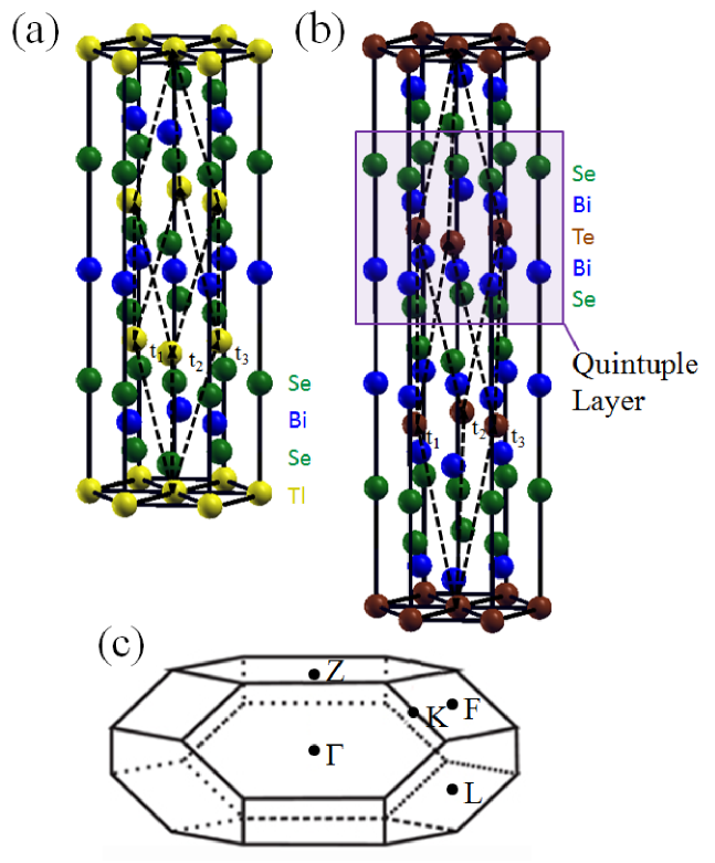
This section details the computational method used, the choice of computational parameters, the bulk crystal structures and the resulting electronic band structure. The bulk crystal structures of both Tl and Bi-based ternary compounds are similar to the binary compounds Bi2X3(X=Se,Te). Both compounds have a trigonal structure with covalently bonded alternating cations and anion layers stacked along the crystallographic z-direction. However, there is one important difference as compared to the binary compounds: The atomic layers of these Tl-based structures are not arranged in a quintuple-like (QL) order, suggesting covalent bonding between the unit-cells, and therefore, that exfoliation techniques, used to peel binary TI flakes from the corresponding bulk crystals, cannot be used for extractng Tl-based TI thin films. The layers are arranged in the order Tl-Se(Te)-Bi-Se(Te). The trigonal unit cell contains four atoms (as opposed to five in binary Bi-based TIs) with the lattice parameter a = 0.7887 nm(0.8263 nm) and the angle between the lattice vectors spanning the lattice of 31.4o(31.8o) for TlBiSe2(TlBiTe2)mahanti . The hexagonal cell, formed from the trigonal, consists of twelve atomic layers with the number of atoms tripled (Fig. 1(a)). The lattice parameters of the hexagonal cell are a=0.4264 nm(0.4534 nm) and c=2.2478 nm(2.3512 nm) for TlBiSe2(TlBiTe2) and the layer sequence in this case is same as the trigonal cell. Compared to the corresponding binary compound, the Bi-based ternary compound Bi2Se2Te (Bi2Te2Se) has one of the Se (Te) layers replaced by a Te (Se) layer, and has the layers arranged in the order Te(Se)-Se(Te)-Bi-Bi-Se(Te). The QL-like layer arrangement in these compounds facilitates exfoliation-like methods which can be used to peel thin films from the bulk-crystals. The lattice parameters of the bulk trigonal cell is almost same for Bi2Se2Te (Bi2Te2Se): a = 1.0046 nm(1.0255 nm) and 24.2o ( 24.1o)nakajima . The hexagonal cell, built from the trigonal structure, contains fifteen atomic layers with the lattice parameters a = 0.422 nm(0.428 nm) and c = 2.92 nm(2.99 nm) for Bi2Se2Te (Bi2Te2Se) (Fig. 1(b)).
We used a DFT-based electronic structure method with projector-augmented wave basisvasp1 and a generalized gradient approximation to the exchange-correlation potentialperdew for computing the electronic properties of the bulk and thin films of both of the compounds. Spin-orbit coupling (SOC) was invoked in the calculation as implemented in the numerical methodvasp2 . For the bulk structural optimizations of both the compounds, a kinetic energy cut-off of 400 eV and a non-orthogonal k-point mesh along the reciprocal lattice vectors of 9 9 9 in the first Brillouin zone (BZ) were chosen. Since previous structural studies of bulk trigonal structures reported agreement with experimental lattice parametersexpt , we chose to relax only the internal parameters, namely the atomic positions, keeping the lattice constants fixed to experimental values. The total energy is assumed to be converged when all the components of Hellman-Feynman forces on each ion are smaller than the threshold 0.001 eV/Å. Convergence of computed properties were carefully checked with respect to large energy cut-off, k-point mesh and larger force threshold. For both the compounds, the computed interlayer distances are quite close to the experimental worksexpt . These computed distances suggest van der Waals type of bonding between the adjacent QLs in ternary Bi-based TI but not in Tl-based TIs. With these informations, we built the bulk hexagonal cell and the corresponding thin-films of both the compounds as detailed in the next section.
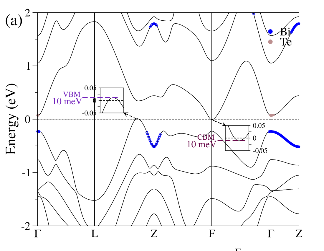
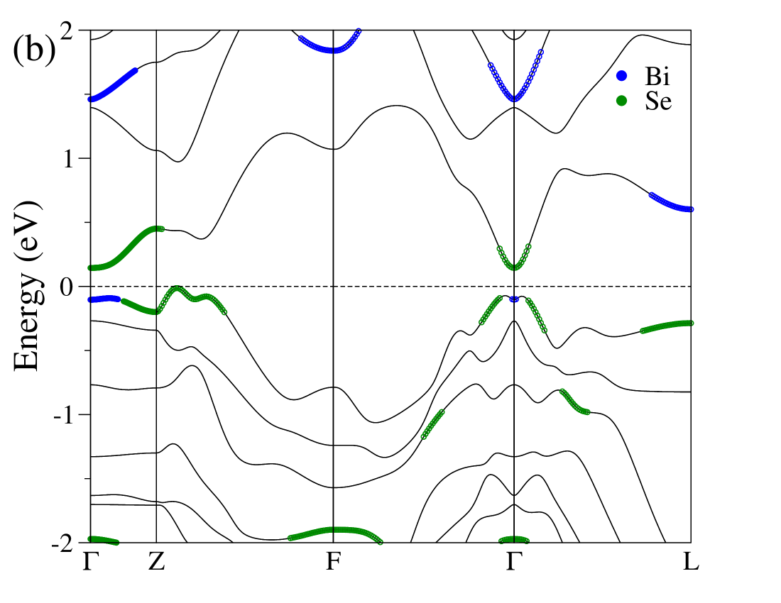
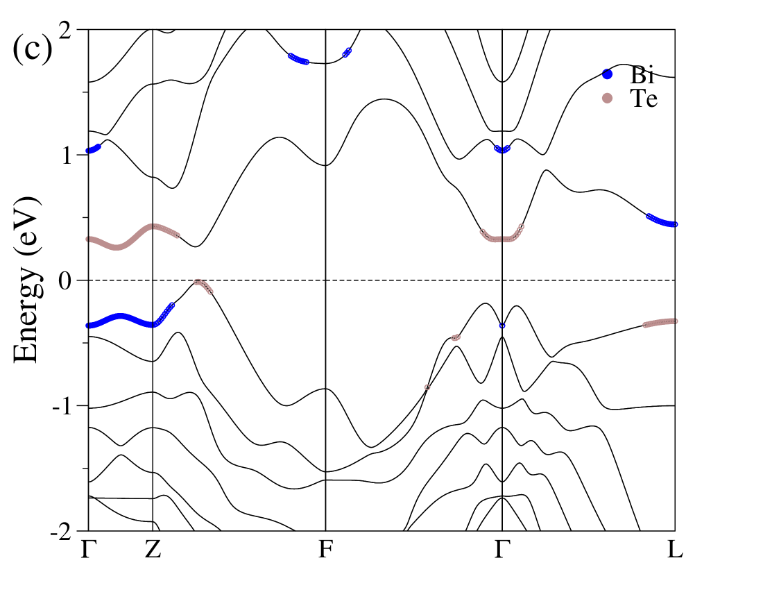
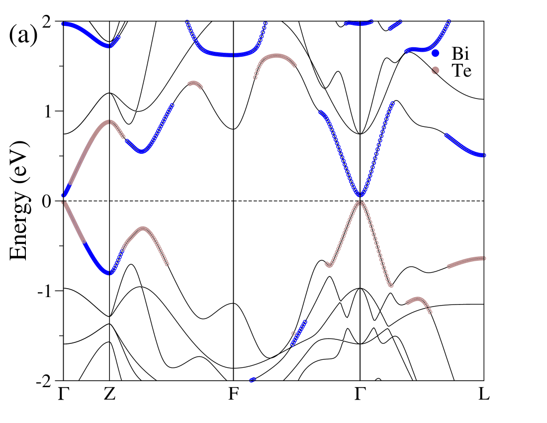

The bulk band structures of TlBiX2 (X= Se,Te), without and with SOC, agree well with other theoretical calculationsmahanti ; mahanti2 . However, with SOC, other calculations predict TlBiTe2 to be an indirect semiconductor with the CB minimum (CBM) at the point and the VB maximum (VBM) on the line joining the L and Z-points. The high-symmetry points are labeled in Fig. 1(c). Recent experimental studies argue TlBiTe2 to be a semimetal with an negative energy gap of 20 meVchen . Our results agree well with this experimental work (Fig. 2(a)). TlBiSe2 has a direct gap at of 124 meV(235 meV) without(with) SOC. Figure 2(b) and (c) show the bulk band structures of Bi2X2Y (X,Y=(Te,Se) or,(Se,Te)) with SOC, which agree quite well with a recent DFT calculationjohnson . The CBM is at the -point and the VBM is between and -points for both the Bi-based TIs. The computed indirect gap are 157 meV and 272 meV, for Bi2Se2Te and Bi2Te2Se, respectively. We note that the gap is direct at the -point without including SOC with the gap values of 633 meV and 76 meV, for Bi2Se2Te and Bi2Te2Se, respectively.
In the literature, emergence of these topological surface states within the bulk band gap of binary 3D TIs was associated with the bulk band inversion when SOC is switched onzahid . We tested this conjecture by plotting the specific orbital contributions from a given atom as a function of k and band on the band structure diagrams of Figs. 2 and 3. These specific contributions are normalized with respect to the contributions from all the orbitals in both the bulk Tl- and Bi-based ternary compounds. Since the bulk CBM and VBM at consist mainly of orbitalsmahanti2 of the Bi and Se(Te) atoms, respectively for Tl-based compounds, this state was chosen for the orbital projection studies. In Tl-based TIs, a cut-off contribution percentage is chosen which gives a reasonable picture of band inversion in these figures. If the calculated orbital contribution of a specific atom at a certain state is greater than a given cut-off percentage, we considered this state as mainly originating from that atom. This cut-off was set at 50 and 25 for Se(Te) and Bi atoms, respectively. A slight change in a cut-off percentage, below or above these choices, resulted in an insignificant change for the CBM and VBM bands at the -point, which is region of interest to study the band inversion process. For example, the orbital contributions on the band structure of TlBiTe2 in Fig. 2(a) remain similar near the CBM and VBM around the -point with the cut-off percentage of 45 and 22.5 for Te and Bi atoms, respectively (Figures not shown). A similar band inversion effect was also seen in Bi-based TIs (Bi2Te2Se and Bi2Se2Te). This effect is shown only for one of the compound Bi2Te2Se (Fig. 3(a) and (b)). The other compounds show similar effects (Figures not shown). We gave an equal weight of 30 to both Bi and Te(Se) orbital contributions since the two outermost layers of Se(Te) and Bi, out of the total of five atomic layers within each QL, mainly particpate in forming the VBM and CBM.
III Thin film band structures and surface states
In this section we discuss the surface states of ternary TIs. First we discuss the interesting nature of surface states in Tl- and Bi-based TIs. We compare our results with binary Bi-based TIs, wherever possible. We choose kinetic energy cut-off of 400 eV and k-mesh size of 9 9 1 on the surface BZ of the hexagonal supercell for computing surface band structure of both Tl- and Bi-based ternary TIs.
III.1 Surface states in Thallium-based ternary compounds
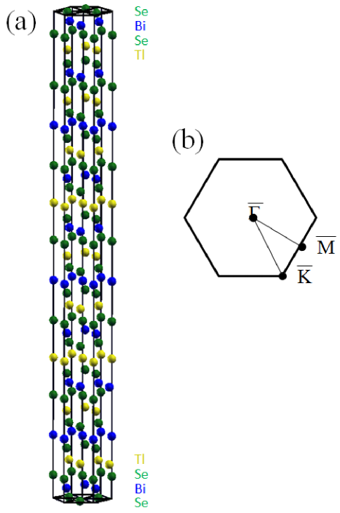
The thin films of Tl-based TIs are built from the bulk hexagonal structure with the atomic layers stacked along the crystallographic z direction and a net vacuum size of 3 nm above the top layer and below the bottom layer within a periodic simulation region. Recent theoreticallin studies suggest contributions to the surface band structure from the dangling bonds arising from the surface terminations, and that these dangling states appear along with the topological surface states. Among four surface terminations, with the atomic layer ordering as Tl-Se(Te)-Bi-Se(Te), Se(Te)-Bi-Se(Te)-Tl, Bi-Se(Te)-Tl-Se(Te) and Se(Te)-Tl-Se(Te)-Bi, the one with Se(Te) beneath the Tl layer is argued to have minimal surface dangling bond densityslin . Therefore we chose this termination in all further thin film studies. We note here that experiments do not observe any signature of dangling bond states in the optical spectraando . And, at least for this termination, we do not find any signature of the dangling bond state either, at least, within the Dirac cone region. Different thicknesses of the thin films of TlBiSe2, ranging from 23 to 39 layers, corresponding to thicknesses of 4 to 7 nm and 23 to 31 layers for TlBiTe2 with the maximum thickness value of 5.8 nm were considered. Figure 4(a) shows a representative supercell structure of 39 layers of TlBiSe2. We consider the relaxation of atomic positions in the z-direction since it is argued that the positions of Se(Te) atoms are critical in determining the topological nature of the surface stateslin . The positions are assumed to be optimized when the z-component of the forces are smaller than the threshold value 0.015 eV/Å.
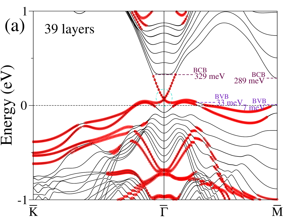
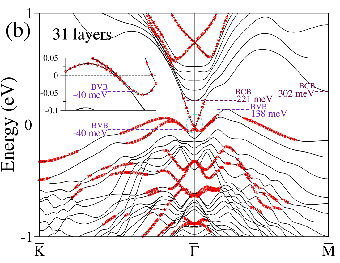
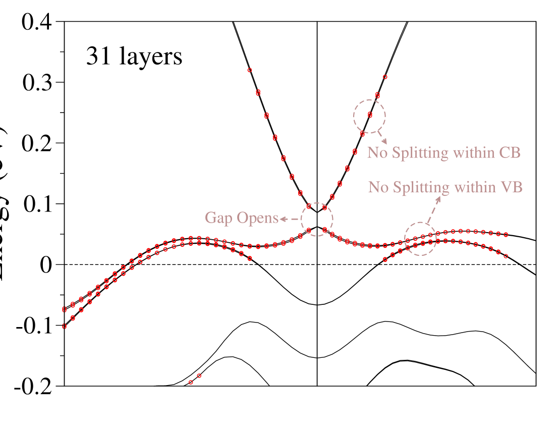
As for the Bi-based binary compounds, Tl-based ternary compounds also show thickness dependent electronic structure. The Dirac cone is preserved in TlBiSe2 with 39 atomic layers, corresponding to a thickness of 7 nm (Fig. 5(a)), and in TlBiTe2 with 31 layers of a thickness 5.8 nm (Fig. 5(b)), where red circles denote surface state contributions and the solid black lines represent the bulk bands. We reproduce the interesting experimental features of TlBiSe2ando and TlBi2Techen . The bulk VB (BVB), in TlBi2Se has two maxima between and M̄ points in the hexagonal BZ (Fig. 4(b)) and the bulk CB (BCB) has a minimum at M̄. The Dirac cone is found to exist inside the bulk band gap, at the -point of the BZ. These features are clearly seen in our computed band structure (Fig. 5(a)). Our computed band structure of TlBiTe2 shows that the Dirac point is below the BVBM (Fig. 5(b)). The BCBM is placed at and the BVBM along the line joining and M̄, producing an indirect gap of 83 meV. Another BVBM emerges along the line joining to K̄. These features including the indirect gap size, positions of BVB, BCB and the Dirac point are consistent with the recent experimental studychen .
For thin film thicknesses corresponding to fewer than 39 (31) atomic layers in TlBiSe2 (TlBiTe2), our study suggests that a band gap opens in the otherwise metallic surface states, much like those in binary Bi-based TIszhang2 . With decreasing thicknesses, the size of the gap seems to increase indicating the increased interactions between surfaces states that exist on two opposite surfaces of the TI (Figures not shown). The gap values are summarized in Table I. There are no experimental reports, so far, on the critical film thickness necessary to preserve the metallic bands for Tl-based ternary TIs which our theoretical study predicts. It is interesting to note that the predicted induced gaps in Tl-based TIs, for the same film thickness, are larger than the binary Bi-based TIs jiwon .
| Number of Layers | 23 | 27 | 31 | 35 | 39 |
|---|---|---|---|---|---|
| E | 0.059 | 0.042 | 0.023 | 0.015 | 0.000 |
| TlBiSe2 | |||||
| E | 0.018 | 0.009 | 0.000 | NA | NA |
| TlBiTe2 |
To understand the origin of the gap at the Dirac point with decreasing film thickness, we first map out the surface state contributions in the band structure from atoms within first few layers of the film, and from all the orbitals, relative to the total contributions of all orbitals from all the layers of the thin film. From the top or bottom surface of the film, 8(6) atomic layers were chosen for TlBiSe2(TlBiTe2). A larger number of atomic layers are used for TlBiSe2 than for TlBiTe2 because a larger number of atomic layers is required to preserve the metallic band structure because the surface states are less localized to the surface region in TlBiSe2. These choices also helped us to choose the same cut-off percentage for both the Tl-based compounds in estimating the surface state contributions. For film thicknesses corresponding to 23, 27, 31, 35 and 39 atomic layers in TlBiSe2, respectively, these cut-offs were varied from 70 - 50, in steps of 5 decrease. For TlBiTe2, 23, 27 and 31 atomic layers were considered with cut-offs of 70, 65 and 60. Examples results of these orbital contributions are marked on the top of the total band structure in Fig. 5(a) and (b).
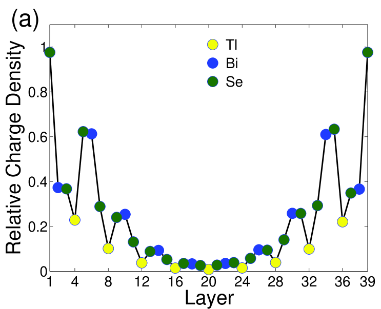
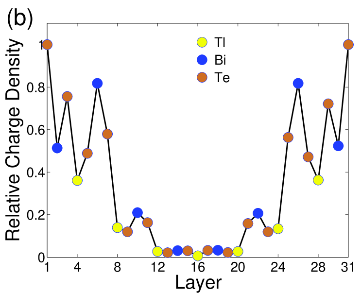
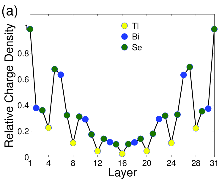
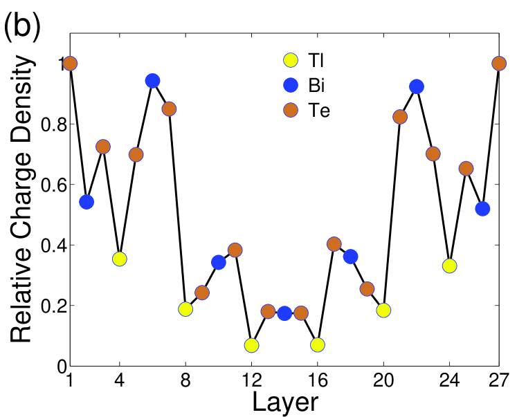
After estimating the distribution of surface states in the thin film structure, we computed the valence charge density resulting from these surface state wave-functions in both the compounds. We focused on surface states around the Dirac-point, in an energy window chosen such that same number of wave-functions are used for building the surface charge density for most relevant thicknesses considered in this study. The wave-functions at three closely spaced k-points including the -point were chosen. The charge density is computed layer-wise. We define the relative charge density, to be the ratio of peak charge density in a particular layer to the peak charge density in all layers. This quantity is plotted in Figs. 7(a) and (b). Our studies suggest exponential decay of the charge density in the bulk region but with slower decay in TlBiSe2 than in TlBiTe2. In about 12-14 atomic layers, from top or bottom surfaces of the film (corresponding to 2.3 nm), the surface state contributions decay to almost zero in TlBiTe2, whereas, the surface states extends up to 16-18 atomic layers (3 nm) in TlBiSe2. With decreasing film thickness, the charge density accumulates in the middle of bulk region in both compounds (Figs. 8(a) and (b)) suggesting increasing interactions of surface states by overlap of their wave-functions inducing a gap at the Dirac point. However, while a band gap is opened in the surface state band structure, away from the surface state band edges band structure is largely unaffected as seen in Fig. 6 -i.e., it does not split into two bands as one would expect from resonant coupling between opposite surface states-suggesting that the splitting is due to interband coupling between the top surface CB and the bottom surface VB and between the top surface VB and the bottom surface CB.
III.2 Surface states of Bismuth-based ternary compounds
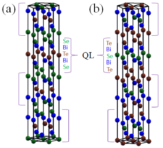
We discuss the surface state properties of Bi2Se2Te and Bi2Te2Se in this section. The building blocks of these compounds are QLs, arranged in the order -Se(Te)-Bi-Te(Se)-Bi-Se(Te)-, and stacked along the crystallographic z-direction (Figs. 9(a) and (b)). Different film thicknesses corresponding the different number of QLs were considered with a maximum of 4 QLs. The choice thickness is guided by the necessity to maintain the metallic nature of the surface bands. The computational parameters used in this study are same as those for Tl-based TIs. We first construct the thin film from experimental parametersnakajima and then study the thin-film properties without and with relaxing the atomic positions with the force convergence criteria of 0.05 eV/Å. The procedure for extracting surface states from crystal wave-functions and the construction of layer-wise surface charge density is same as that for Tl-based TIs discussed in the previous section.
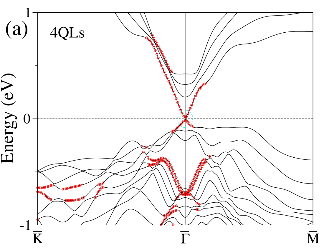
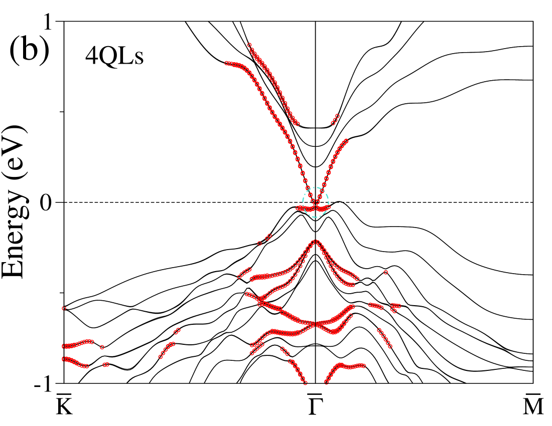
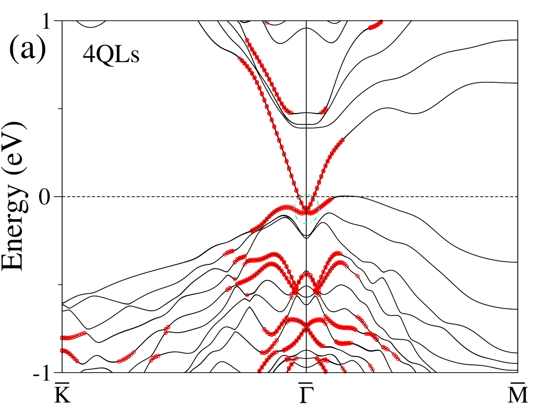
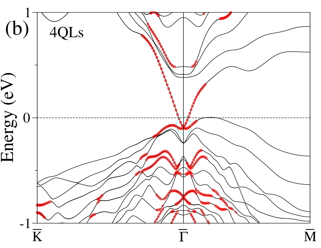
The thin-film structure of Bi2Se2Te, without internal position relaxation, shows a more symmetric Dirac cone with metallic bands, as compared to the Tl-based TIs for thickness corresponding to 4 QLs (Fig. 10 (a)). The bulk band gap (of 313 meV) supports these novel states, and the Dirac point is well within this gap. Recently, a report of 3 QLs, as the minimum thickness, required to preserve the Dirac cone has appearedjohnson . We find 4 QLs to be necessary, which we also illustrate with the help of surface charge density calculations. However, in the absence of any experimental work, it is likely that the minimum thickness, carefully predicted by different theoretical methods, may fall in the range of 3QLs-4QLs. For film thicknesses below 4 QLs, a finite gap is induced at the Dirac point whose size increases with decreasing the film thickness (Figures not shown). The size of the gap values are listed in Table II. With atomic relaxation, the Dirac cone is affected and its symmetry is lost (Fig. 10(b)). The BVB lies along the line joining and M̄ in the hexagonal BZ, and its maximum is positioned almost in line with the Dirac point. This hints at crucial role played by rearrangement of atomic positions either insitu in thin-film preparation procedure or in presence of external environments. In Bi2Te2Se, a significant part of surface state band structure falls below the BVBM and the Dirac point occurs in the energy neighborhood of the -point. Atomic relaxation has almost negligible effect on the overall band structure (Figs. 11 (a) and (b)) in this case. Decreasing film thickness induces a finite gap (Table II). These studies suggest that the Dirac cone remains protected in thinner layers of ternary Bi-based TIs than in binary Bi-bsed TIs or than in Tl-based TIs.
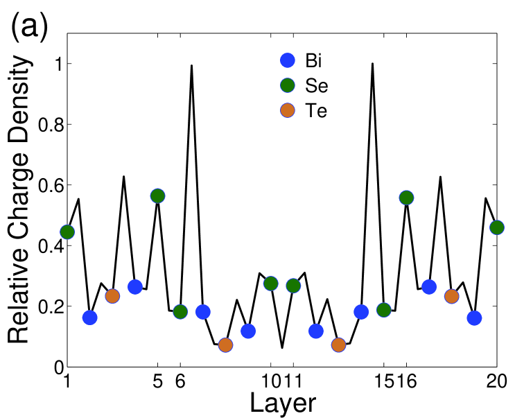
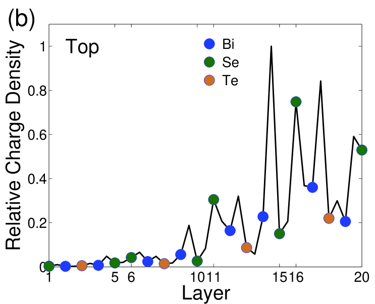
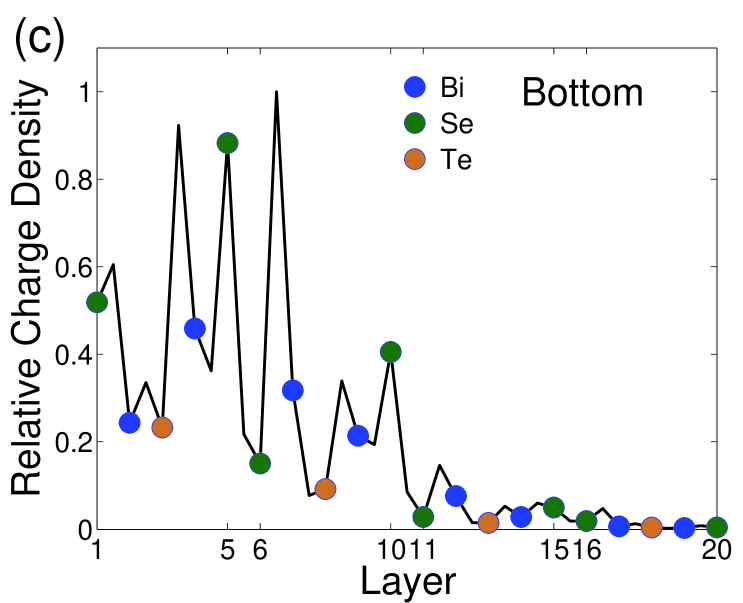
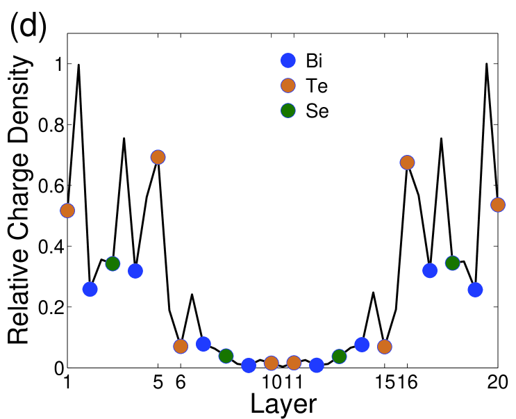
The origin of the critical thickness needed to maintain the metallic nature of the surface states can be understood by studying the layer-dependent surface charge densities. The procedure is same as that used for Tl-based TIs, except the charge density in the interstitial regions is also considered in order to locate the surface state spread in the bulk region as precisely as possible for thinner films thicknesses. For 4 QL thick Bi2Se2Te films, the combined charge density from the surface states of both sides of the film seems to be significant in the middle of the bulk region (Fig. 12(a)). However, we separately computed the charge densities resulting from top and the bottom surface states. As seen from the plots (Figs. 12(b) and (c)), the density associated with surface states drops rapidly beyond 2 QLs, indicating negligible interaction between these opposite surface states in the 4QL film, consistent with the observed protected Dirac cone. Relaxation of atomic positions is found to have no significant effect. In the 4QL films of Bi2 Te2 Se, even the combined contribution from both surfaces is small in our studies with and without atomic relaxation (Figs. 12(d)).
| Number of QLs | 2 | 3 | 4 |
|---|---|---|---|
| E | 0.128 | 0.038 | 0.000 |
| Bi2Se2Te without relaxation | |||
| E | 0.086 | 0.017 | 0.000 |
| Bi2Se2Te with relaxation | |||
| E | 0.039 | 0.037 | 0.000 |
| Bi2Te2Se without relaxation | |||
| E | 0.027 | 0.037 | 0.000 |
| Bi2Te2Se with relaxation |
IV Summary and Conclusions
We use a density functional based electronic structure method to study the thin film surface state properties of Tl and Bi-based ternary topologicial insulators. These studies predict that the Dirac cone remains protected in thinner layers of ternary Bi-based TIs than in binary Bi-based TIs or than in Tl-based TIs, which may be advantageous for certain applications. However, we also predict that in the atomically relaxed strucures, the Dirac cone of all but Bi2Se3 lie in or near the BVB. However, the Dirac cone of Bi2Se2Te remains outside of the BVB in the absence of relaxation, as might occur with dielectrics replacing the air gap. And, of course, the bonding to the dielectric could directly affect the surface states as well. Our computed results agree very well with experimental results where available, while other predictions such as the critical film thicknesses required to maintain the Dirac cone, size of the induced gaps, and the extent of the spread of surface states in the bulk region point to further needed experimental work.
Acknowledgements.
The authors acknowledge financial support from the Nanoelectronics Research Initiative supported Southwest Academy of Nanoelectronics (NRI-SWAN) center. We thank the Texas advanced computing center (TACC) for computational support (TG-DMR080016N).References
- (1) X.-L. Qi and S.-C. Zhang, Physics Today 63, 33 (2010); X.-L. Qi and S. -C. Zhang, arXiv:1008.2026; M. Z. Hasan and C. L. Kane, Rev. Mod. Phys 82, 3045 (2010); M. Z. Hasan and J. E. Moore, Annual Review of Condensed Matter Physics (Jan. 2011); X. Zhang, J. Wang and S.-C. Zhang, Phys. Rev. B 82, 245107 (2010); D. Culcer and S. Das Sarma, arXiv:1012.3459; R. Yu, W. Zhang, H. J. Zhang, S. C. Zhang, X. Dai, Z. Fang, Science 329, 61 (2010)
- (2) Y. L. Chen, J. G. Analytis, J. -H. Chu, Z. K. Liu, S. -K. Mo, X. L. Qi, H. J. Zhang, D. H. Lu, X. Dai, Z. Fang, S. C. Zhang, I. R. Fisher, Z. Hussain, Z. -X. Shen, Science 325, 178 (2009), Y. Xia, D. Qian, D. Hsieh, L. Wray, A. Pal, H. Lin, A. Bansil, D. Grauer, Y. S. Hor, R. J. Cava, M. Z. Hasan, Nature Physics 5, 398 (2009). Y. -Y. Li, G. Wang, X. -G. Zhu, M. -H. Liu, C. Ye, X. Chen, Y. -Y. Wang, K. He, L. -L. Wang, X. -C. Ma, H. -J. Zhang, X. Dai, Z. Fang, X. -C. Xie, Y. Liu, X. -L. Qi, J. -F. Jia, S. -C. Zhang and Q. -K. Xue, Adv. Mater. 22, 4002 (2010). C.-Z. Chang, K. He, M. -H. Liu, Z. -C. Zhang, X. Chen, L. -L. Wang, X.-C. Ma, Y.-Y. Wang and Q.-K. Xue, arXiv:1012.5716; A. Richardella, D. M. Zhang, J. S. Lee, A. Koser, D. W. Rench, A. L. Yeats, B. B. Buckley, D. D. Awschalom, N. Samarth, arXiv:1012.1918 (to appear in Appl. Phys. Lett.)
- (3) H. Steinberg, D. R. Gardner, Y. S. Lee, P. J. -Herrao, Nano Lett. 10, 5032 (2010); B. Sacepe, J.B. Oostinga, J. Li, A. Ubaldini, N.J.G. Couto, E. Giannini, A.F. Morpurgo, arXiv:1101.2352; I. Appelbaum, H. D. Drew, M. S. Fuhrer, Appl. Phys. Lett. 98, 023103 (2011)
- (4) H. Lin, L. A Wray, Y. Xia. S. Y. Xu, S. Jia, R. J. Cava, A. Bansil, M. Z. Hasan, Nat. Mat. 9, 546 (2010), S. Chadov, X. Qi, J. Kübler,G. H. Fecher, C. Felser, S. C. Zhang, Nat. Mat. 9, 541 (2010); O. V. Yazyev, J. E. Moore and S. G. Louie, Phys. Rev. Lett. 105, 266806 (2010).
- (5) J. Xiong, A. C. Petersen, D. Qu, R. J. Cava, N. P. Ong, arxiv:1101:1315; Z. Ren, A. A. Taskin, S. Sasaki, K. Segawa, Y. Ando, Phys. Rev. B 82, 241306(R) (2010).
- (6) M.Z. Hasan, H. Lin, A. Bansil, Physics 2, 108 (2009); L. Fu, Phys. Rev. Lett 103, 266801 (2009).
- (7) T. Sato, K. Segawa, H. Guo, K. Sugawara, S. Souma, T. Takahashi, Y. Ando, Phys. Rev. Lett. 105, 136802 (2010); K. Kuroda, M. Ye, A. Kimura, S.V. Eremeev, E. E. Krasovskii, E.V. Chulkov, Y. Ueda, K. Miyamoto, T. Okuda, K. Shimada, H. Namatame, and M. Taniguchi, Phys. Rev. Lett. 105, 146801 (2010).
- (8) H. Lin, R.S. Markiewicz, L.A. Wray, L. Fu, M.Z. Hasan, A. Bansil, Phys. Rev. Lett. 105, 036404 (2010);
- (9) S. Souma, K. Kosaka, T. Sato, M. Komatsu, A. Takayama, T. Takahashi, M. Kriener, Kouji Segawa, Yoichi Ando, arXiv:1101.3421;
- (10) S. -Y. Xu, L. A. Wray, Y. Xia, R. Shankar, S. Jia, A. Fedorov, J.H. Dil, F. Meier, B. Slomski, J. Osterwalder, R.J. Cava, M.Z. Hasan, arXiv:1008.3557.
- (11) Y. L. Chen, Z. K. Liu, J. G. Analytis, J.-H. Chu, H. J. Zhang, B. H. Yan, S.-K. Mo, R. G. Moore, D. H. Lu, I. R. Fisher, S. -C. Zhang, Z. Hussain, Z. -X. Shen, Phys. Rev. Lett 105 266401 (2010).
- (12) G. Kresse and J. Furthmuller, Comp. Mater. Sci. 6, 15 (1996); G. Kresse and J. Furthmuller Phys. Rev. B 54, 11169 (1996); G. Kresse and D. Joubert Phys. Rev. B 59, 1758 (1999).
- (13) J. P. Perdew, K. Burke and M. Ernzerhof, Phys. Rev. Lett. 77, 3865 (1996).
- (14) D. Hobbs, G. Kresse, and J. Hafner, Phys. Rev. B 62, 11556 (2000).
- (15) K. Hoang and S. D. Mahanti, Phy. Rev. B 77,205107 (2008).
- (16) E. F. Hockings and J. G. White, Acta Crystallogr. 14, 328 (1961); O. Madelung, Semiconductors: Data Handbook. 3rd Ed. (Springer, Berlin, 2004), and references therein .
- (17) B. Yan, C. X. Liu and S. C. Zhang, Europhys. Lett. 90, 37 002 (2010), S.V. Eremeev, Yu. M. Koroteev, and E. V. Chulkov, JETP Lett. 91, 594 (2010)
- (18) L. -L. Wang and D. D. Johnson, arXiv:1012.3974
- (19) H. Zhang, C. -X. Liu, X. -L. Qi, X. Dai, Z. Fang and S.-C. Zhang, Nat. Phys. 5, 438 (2009).
- (20) J. Chang, P. Jadaun, L. F. Register, S. K. Banerjee and B. Sahu, arXiv:1012.2927
- (21) S. Nakajima, J. Phys. Chem. Solids 24, 479 (1963)